Efficient FPGA Implementation of the Basic Receiving
Functions for Aeronautical Reconfigurable Data-Link
Angelo Manco
Embedded Systems and Communications Lab C.I.R.A. ItalianAerospaceResearchCenter
Via Maiorise -81043 - Capua, Italy
Vittorio Ugo Castrillo
Embedded Systems and Communications Lab C.I.R.A. Italian AerospaceResearch Center
Via Maiorise - 81043 - Capua, Italy
ABSTRACT
The paper focuses on the efficient FPGA implementation of the baseband receiving functions for a Reconfigurable Data-Link (RDL). A binary CP-FSK case study is considered to show the model-based approach. The design is then imple-mented and tested on low cost FPGA.
General Terms
SDR based reconfigurable communication systems.
Keywords
Synchronization, SoftwareDefined Radio, CP-FSK Demodu-lation, Model-based Design
1.
INTRODUCTION
Some of current and future challenges in Unmanned Aerial Vehicles aeronautical communications, like environment link adaptation and multi-standard operations, require flexibility and scalability for the communication systems. These re-quirements can be addressed developing a Reconfigurable Data-Link (RDL), which is a system able to provide different communication functions to the user without changing hard-ware. To design such a system, a model-based approach and SDR paradigm are investigated.
Model-based approach is helpful to obtain modular architec-tures with stand-alone blocks which can be used afterwards for other systems designs simply changing their interconnec-tions. Therefore one of the main goals is the development of a library of blocks (each one with its own close hardware mod-el) useful to implement a RDL.
Pushing the analog-to-digital conversion as close as possible to the antenna, SDR based systems allow to realize multiple radio features on the same hardware platform and to adapt the designed communications system to the radio context changes. In this panorama, Field-Programmable Gate Arrays (FPGAs) show good balance among computational power, configurability and design costs, so they are suitable to realize the advanced signal processing tasks necessary in the physical layer of a SDR based system.
On the basis of the above considerations, this paper focuses on the design and the FPGA implementation of basic receiv-ing functions as part of a complete RDL usreceiv-ing a model-based approach. Since Continuous Phase Modulations (CPM) play an important role in the area of aeronautical communications, in particular in the telemetry field, the receiving functions are investigated for a binary CP-FSK demodulator case.
The efficient implementation has a key role, then algorithms that are suitable for low cost FPGA are considered.
Digital signal processing can be executed at high or interme-diate frequencies, but baseband processing is much more suit-able by hardware performance and cost point of view; there-fore in this work all operations are done on in-phase (I) and on quadrature (Q) components coming from a down conversion stage (heterodyne or homodyne) that is not described here. Synchronization is taken into account and feedback solutions are adopted. In particular, both timing and carrier recovery are implemented as described in sections IV and V. A model-based design approach is adopted in this project as described in section VI. Simulation results and implementation details are provided in sections VII and VIII. Lastly, tests on hard-ware platform are illustrated in section IX.
2.
BACKGROUND
A Continuous Phase FSK modulated signal is described by the following equation:
2 () 0
cos 2 )
( ftt
T E t
s c
s (1)
where Es is the symbol energy, T the symbol period, fc the carrier frequency, φ(t) the phase due to frequency modulation and φ0 is a constant phase term. In a continuous phase mod-ulation there are no phase discontinuities between symbols, so the frequency modulation term is
a t dT h t
t
i() )
(
0
(2)
where h is the modulation index and ai are the symbols, be-longing to {-1, 1} for a binary FSK.
2 ( )
2 sin
()
sin 2 ) ( ) ( cos 2 ) ( 2 cos 2 ) ( 0 0 t T E t f f T E t Q t T E t f f T E t I s s i s s s i s (3)
[image:2.595.318.551.87.163.2]where φs(t)is the phase of I/Q vector. In (3) we have consi-dered, in place of φ(t), the frequency fi, that is the frequency separation h/2T multiplied for the symbol ai, and Δfwhich is the frequency drift due to mismatch between carrier frequency and local oscillator frequency of the quadrature mixer in the down conversion stage. The I/Q signals are sampled by an ADC (see Figure 1), with a sampling period Ts equal to T/N, where N is the number of samples for symbol, and then processed by the demodulator.
Figure 1: CP-FSK base band demodulator functional ar-chitecture
The determination of demodulated data bits involves the cal-culation of the I/Q vector phase φs, the calculation of the fre-quency fi related to the transmitted symbol and the use of a bit decision block based on fi value. Two feedback structures are used for synchronization: a bit timing recovery loop and a car-rier recovery loop (in order to have a coherent demodulation through the elimination of the drift Δf). These functions will be illustrated in the following sections.
3.
FREQUENCY CALCULATION AND
BIT DECISION
In order to calculate the instantaneous phase of the I/Q vector a Phase Detector (PD) is necessary; this functional block computes a translation from rectangular coordinates (i.e. the I/Q components) to polar ones (phase φs and the magnitude of the I/Q vector). For this purpose a CORDIC (COordinate Ro-tation DIgital Computer) algorithm in vectoring mode is used [1]. It is an iterative procedure that only needs of adders, bar-rel shifters and a look-up table with off-line calculated values [2] and, therefore, well suited for low cost FPGAs where ded-icated multiplier resources are limited. Since the algorithm doesn’t converge for input vectors having phase (in module) greater than 99°, a range extension is used [3]. In the demodu-lator design a 5 stages, 11 bit precision, unfolded CORDIC processor is implemented.
The CORDIC output phase is used to calculate the frequency information by means of the phase difference between a sam-ple and the preceding one, followed by a phase unwrap opera-tion (to remove phase discontinuities) and a time scaling (see Figure 2).
Figure 2: Frequency calculation
The overall structure forms a Frequency Detector (FD) that performs the CP-FSK demodulation, starting from baseband I/Q signals, with a fully pipelined architecture.
Finally, the bit decision is computed using a zero threshold comparator taking in account that the demodulated frequency fi ideally should assume two opposite values (±h/2T).
4.
BIT TIMING RECOVERY
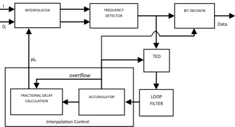
[image:2.595.58.279.226.328.2]The sampling period of analog-to-digital converter in the down-conversion stage is not aligned to the symbol period, i.e. it is asynchronous with symbols, and so timing errors af-fect demodulation performance in presence of noise. Real-world symbol pulse shapes have a peak in the centre of the symbol period. Sampling the symbol at this peak means to have the best signal-to-noise-ratio and it will mitigate interfe-rence from other symbols. There are possible several ap-proaches to fix this issue depending on the characteristics of the receiver. We consider the case where the timing correction is all digital. This means that it is not possible to adjust the sampling frequency/phase of the ADC (it is fixed), passing from digital domain to analog one. A feedback scheme is adopted and in particular a non-data-aided (NDA) timing re-covery technique is used [4][5][6][7]. The structure is de-picted in Figure 3.
Figure 3: Bit timing recovery loop
I
Q
INTERPOLATOR FREQUENCY
DETECTOR BIT DECISION FRACTIONAL DELAY CALCULATION TED LOOP FILTER ACCUMULATOR Interpolation Control Data Bits μk overflow I Q PHASE DETECTOR (CORDIC) PHASE DIFFERENCE PHASE UNWRAPPER TIME SCALING FREQUENCY DETECTOR FREQUENCY CALCULATION
φs fi
I
Q
ADC
RE-SAMPLING PHASE CALC FREQUENCY CALC BIT DECI SION TIMING RECOV-ERY CARRIER RECOVERY
LOOP CPFSK demodulator
[image:2.595.319.555.473.601.2]Let are {..., (k-1)T, kT, (k-1)T, ...} the desired interpolation instants and {..., (n-1)Ts, nTs, (n-1)Ts, ...} the ADC sampling instants with n ≈ kN. The right sample for the k-th symbol is computed by means of an interpolation of ADC I/Q output samples on the basis of the fractional delay μk and on the last L samples available from ADC, where μk is the distance be-tween the desired optimum sample (i.e. the sample at the time kT) and the closest ADC preceding sample (whose index, in-dicated with mk, is named base-point index) and L depends on the interpolation order. For example, the interpolated Q com-ponent sample is:
) ) ((
)
(kTi q mk k Ts
q (4)
[image:3.595.63.274.336.426.2]A Lagrange polynomial interpolation is considered. Since the Lagrange coefficients are expressed as a polynomial in μ, the interpolation is implemented as Farrow structure [8][9]. This approach allows the fractional delay to vary in a continuous way. In order to further reduce the area occupancy, a modified structure is used. Considering that some coefficients are re-peated as shown in table I, it is possible to forward the result of the multiplication to the tap where the same coefficient (or its 2’s power) is present, avoiding in this way an operation.
Table 1: Filter Coefficients for Cubic Lagrange Polyn.
i Filter coefficients
m=0 m=1 m=2 m=3
-2 0 -1/6 0 1/6
-1 0 1 1/2 -1/2
0 1 -1/2 -1 1/2
1 0 -1/3 1/2 -1/6
So the amount of multiplicators passes from 4 to 1, realizing a more efficient architecture.
A Timing Error Detector (TED) is used to estimate the error between the right sampling instant and the current one. In par-ticular the Gardner algorithm is used. It is based on finding zero crossing between two consecutive symbols. The demodu-lated CP-FSK signal has the right shape to be considered suit-able for the Gardner algorithm. It uses two samples per sym-bol and it generates the following error signal:
( ) (( 1) )
(( 12) )) (
ˆkTi y kTi y k Ti y k Ti
e (5)
In our case the TED works at the sampling rate (1/Ts) and so its output is decimated according to the base-point index mk to extract the right error.
The TED output is filtered in order to have the control signal for the timing adjustment. A second order Proportional-plus-Integrator (PI) loop filter is used for this purpose. In particular it consists of two paths. The proportional path multiplies the error signal by the proportional gain Kp. It is able to track out a phase step error. An integral path multiplies the error signal by the integral gain Ki in order to track out a ramp phase error (i.e. a frequency error). Constants Kp and Ki can be calculated considering a certain dumping factor ζ and an equivalent noise bandwidth Bnusing a procedure similar to the one of a PLL (Phase Locked Loop) design as explained in [8]. Note that the gain of the linearized TED and the NCO gain must be known to make the above procedure.
The Interpolation Control provides the base-point index and the fractional delay on the basis of the filtered error signal
v(kTi). It is performed by a Numerically Controlled Oscillator (NCO) [5]. In this case, the NCO is constituted by an accumu-lator, operating at the sampling rate 1/Ts, that overflows every N samples. The overflow in the k-th period is the trigger that indicates the base-point mk. The loop filter output v(kTi) ad-justs the amount by which the accumulator increments. The fractional delay is computed using the content η of the accu-mulator as showed in the following equation [5]:
) ( )
(mk N mk
(6)
The fractional delay is updated at symbol rate.
5.
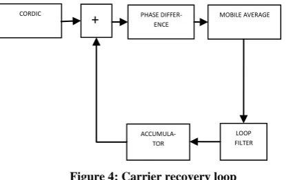
CARRIER RECOVERY
The carrier recovery is based on a second-order frequency control loop composed by a NCO and a PI filter (Figure 4). The CORDIC output phase can be used as loop input. The frequency information associated to the symbols has to be subtracted by the samples phase difference so that only the frequency error is compensated by the loop; this operation is accomplished using a mobile average implemented with a Cascaded Integrator-Comb (CIC) filter. We suppose that the data stream transmitted is random and balanced, in other words it contains an equal number of 0’s and 1’s; in this case the mobile average output is roughly equal to the frequency drift respect to the carrier multiplied by the sampling time. A proper number of registers should be used for the CIC filter implementation to have a good trade-off between logic ports consumption and good performances in terms of residual fre-quency drift.
In this case NCO is a simple accumulator with a unitary DC gain and no initial frequency offset. Its output can be used to compensate the samples phase outgoing from the CORDIC processor.
Figure 4: Carrier recovery loop
Lastly, PI loop filter constants Kp and Ki can be calculated considering a certain dumping factor ζ and an equivalent noise bandwidth Bn expressed in terms of maximum frequency drift Δfmax loop can track, using the following formula [8]:
2 2m ax
f
Bn (7)
where Δfmaxis bounded by the following constraint:
T N N
h f
2 1
m ax
(8)
taking into account a 20% of safe margin in the implementa-tion stage. Anyway tracking errors are proporimplementa-tional to the equivalent noise bandwidth, so the optimum choice for the right value of Bn has to be based on a trade-off between fast acquisition and good tracking [8].
CORDIC PHASE
DIFFER-ENCE
MOBILE AVERAGE
(CIC FILTER)
+
LOOP FILTER
[image:3.595.317.525.428.559.2]6.
DESIGN FLOW
[image:4.595.324.524.81.231.2]CP-FSK base-band demodulator design is composed by the following steps. First of all the demodulator is high-level modelled and tested in MATLAB/SIMULINK environment. Required functions are implemented using standard maths functions (as the arctangent for the extraction of the phase in-formation) and all signals are represented with a double data type. In the second step a close hardware model is designed. The general maths functions are calculated with algorithms whose hardware implementations are convenient (for example SIMULINK arctangent block is replaced by a custom vector-ing CORDIC processor). Durvector-ing the third step the data type is changed to fixed-point in order to obtain blocks models struc-ture well suited to get a VHDL code. At this stage, comparing the simulation results of the double data type blocks models and the ones related to fixed-point models, it is possible to determinate the best choice for words and fractional parts lengths, choosing a good trade-off between accuracy and re-sources utilization. At the fourth step a VHDL code is de-signed for each block and for the overall system, taking into account the FPGA target. The fifth step is relative to simula-tion of demodulator VHDL code using SIMULINK and co-simulation tools; Next, an hardware test using true external CP-FSK transmitter and BER tester. In a final step, perform-ance tests will be executed to estimate the demodulator qual-ity in presence of carrier frequency and timing errors.
Figure 5: Design flow
7.
SIMULATION
The overall system is simulated in MATLAB/SIMULINK environment. The aim of the simulation is to verify that the demodulator, in particular the synchronization functions, works properly. Timing and carrier errors are considered sep-arately.
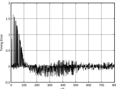
[image:4.595.326.522.286.437.2]The coefficients of the loop filter for the timing recovery are designed considering an unitary damping factor and a single-sideband noise bandwidth Bn of 0.5% of the symbol rate. A PN11 bit sequence is generated through a Linear Feedback Shift Register and used, after modulation, as data input of the system. Whereas the sampling period of analog-to-digital converter in the down-conversion stage is not aligned to the symbol period, a step timing error is firstly considered. No carrier errors are introduced. Figure 6 and Figure 7 show the transient responses of the fractional delay μk and of the TED error signal. The fractional delay μk reaches a steady-state value of 0.85 (i.e. the target value) after about 500 symbols.
Figure 6: Fractional delay transient response for a step timing error
Figure 7: TED transient response for a step timing error
Response to a timing error ramp of 1% of symbol period is shown in Figure 8 and Figure 9. The TED error signal goes to zero thanks to the second order loop filter that is capable to track out a frequency error. Because a residual timing error accumulates, the fractional delay μk decreases with time [8]. When the accumulated residual timing error exceeds a sample period, μk wraps around to 1. It happens every 100 symbols, accordingly to the introduced error.
Figure 8: Fractional delay transient response for a ramp timing error
0 100 200 300 400 500 600 700 800 0
0.1 0.2 0.3 0.4 0.5 0.6 0.7 0.8 0.9 1
t/T
Fr
a
c
ti
o
n
a
l
D
e
la
y
k
0 100 200 300 400 500 600 700 800 -0.5
0 0.5 1 1.5 2
t/T
Ti
m
in
g
E
rr
o
r
0 100 200 300 400 500 600 700 800 0
0.1 0.2 0.3 0.4 0.5 0.6 0.7 0.8 0.9 1
t/T
Fr
a
c
ti
o
n
a
l
D
e
la
y
[image:4.595.55.278.364.527.2] [image:4.595.324.524.572.721.2]Figure 9: TED transient response for a ramp timing error
[image:5.595.328.522.81.229.2]The behavior of the carrier recovery loop is also examined. The coefficients of the loop filter are designed considering a damping factor ζ = 1/√2 and a single-sideband noise band-width Bn of 5% of the symbol rate. The size of the mobile average window is 256 symbols long. Figure 10 shows the response to the step error; in particular, the frequency error is 70% of the Δfmax accordingly to the equation (8). The carrier can be considered locked when the frequency error is 1/16th of the symbol rate. The steady-state error is not zero because of the approach used for the detection of the frequency offset (symbols are never perfectly balanced). Figure 11 shows how the offset of the demodulated signal, which is normalized to the frequency separation, is corrected after about 500 sym-bols.
[image:5.595.64.263.428.577.2]Figure 10: Carrier recovery loop response
Figure 11: Frequency offset correction for a step error
8.
IMPLEMENTATION
The data are processed at a sample rate of exactly four times the symbol rate, in other words for each symbol there are four samples. This level of granularity is sufficient thanks to the use of the cubic interpolation, that allows fine resampling. Note that if a linear interpolator was used, an higher sample rate would be necessary to achieve the same result in term of accuracy.
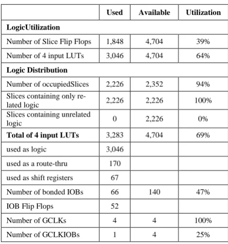
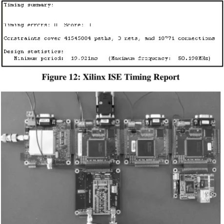
The demodulator is implemented on a COMBLOCK© 1000 demo-board (Figure 13) equipped with a very low cost Xilinx Spartan II X2CS200 FPGA. Table II shows the resources uti-lization and Figure 12 shows the maximum operating fre-quency.
Table 2: Resources utilization
Used Available Utilization
LogicUtilization
Number of Slice Flip Flops 1,848 4,704 39%
Number of 4 input LUTs 3,046 4,704 64%
Logic Distribution
Number of occupiedSlices 2,226 2,352 94% Slices containing only
re-lated logic 2,226 2,226 100%
Slices containing unrelated
logic 0 2,226 0%
Total of 4 input LUTs 3,283 4,704 69%
used as logic 3,046
used as a route-thru 170
used as shift registers 67
Number of bonded IOBs 66 140 47%
IOB Flip Flops 52
Number of GCLKs 4 4 100%
Number of GCLKIOBs 1 4 25%
0 100 200 300 400 500 600 700 800 -1.5
-1 -0.5 0 0.5 1 1.5 2
t/T
Ti
m
in
g
E
rr
o
r
0 200 400 600 800 1000 1200 1400 1600 1800 2000 -20
0 20 40 60 80 100
t/T
Fr
e
q
u
e
n
c
y
E
rr
o
r
[H
z
]
0 200 400 600 800 1000 1200 1400 1600 1800 2000 -2
-1 0 1 2 3 4 5
t/T
N
o
rm
ili
z
e
d
Fr
e
q
u
e
n
c
[image:5.595.309.544.430.682.2]Figure 12: Xilinx ISE Timing Report
Figure 13: Comblock modules used for the tests
Note that part of the design is occupied by the glue-logic for the communications with the microcontroller present on the demo-board. The commercial module provided by COM-BLOCK© allow us to rapid prototype the demodulator design. In fact it is compatible with COMBLOCK© 3001-A RF front-end that operates the RF to baseband conversion and the ana-log to digital one of the I/Q samples. The two boards shared the same 40MHz clock source for synchronous data transfer-ring. The dual Analog-to-Digital Converter has a sample rate of 40MSamples/s and 10bits of resolution for I/Q samples [10]. In this case the maximum data rate is 9.9Mbps consider-ing a 1% of safe margin. The data rate is defined at run time configuring some register of the microcontroller through cus-tom software and RS-232 communication.
9.
TESTING
For testing purpose a Rhode & Schwarz SMU-200A signal generator has been used. It is capable to generate an RF mod-ulated signal. The settings are:
• FSK modulation with modulation index h = 0.7 • Data-rate R = {200 kbps, 9 Mbps}
• Pseudo-random source sequence PN-11 • Carrier frequency f0 = 2.315GHz • Signal power at the output Pout = -68dBm
The generator is linked to the RF down-conversion stage through a coaxial cable and a BER tester (COMBLOCK© 1005 module) is used to validate the system.
In Figure 14 the I signal, the interpolated and resampled I sig-nal, the bit clock signal and the data bits are respectively shown.
Figure 14: Acquisition screenshot of internal signals
In Figure 15 the fractional delay is depicted. The saw-tooth waveform indicates a frequency error between the clock at the transmitter (i.e. the signal generator) and at the receiver.
Figure 15: Acquisition screenshot of the fractional delay signal
It is possible to add a frequency offset to the carrier in order to test the frequency recovery performances. The maximum car-rier frequency error that the demodulator is capable to track is ± 225 kHz, in according to simulation results.
[image:6.595.316.543.326.494.2]10.
CONCLUSIONS
In this paper, basic receiving functions of a communication system were investigated for a CP-FSK base-band demodula-tor case with the aim to create a library of modular blocks that can be used to implement a Reconfigurable Data-Link. A model-based approach was used in the design flow. In such way the transition from a high level blocks models to a close hardware ones was simplified and the development time was considerably reduced. The obtained models were tested with software simulation showing a proper operation. The VHDL code is generated and implemented on low cost FPGA. The demodulator is successfully tested with laboratory instrumen-tation.
11.
REFERENCES
[1] Rice Michael, Padilla Marc, Nelson Brent, “On FM De-modulators in Software Defined Radios Using FPGAs”, Grant no. 0801876, I/UCRC Program of the National Science Foundation, Provo, Utah, October 2009
[2] Volder Jack, “The CORDIC trigonometric computing technique”, IRE Transactions on Electronic Computers, vol. 8, no. 3, September 1959, pp. 330-334
[3] Andraka Ray, “A survey of CORDIC algorithms for FPGA based computers”, Proceedings of the ACM/SIGDA sixth international symposium on Field programmable gate arrays, Monterey, CA, February 22-24 1998, pp. 191-200
[4] Meyr Heinrich, Moeneclaey Marc, Fechtel Stefan A., “Digital Communication Receivers, Synchronization, Channel Estimation and Signal Processing”, vol. 2, Wiley, NY, November 1997
[5] Gardner Floyd, “Interpolation in Digital Modems – Part I: Fundamentals, IEEE Transactions on Communica-tions, vol. 41, no. 3, March 1993, pp. 501 – 507
[6] Erup Lars, Gardner Floyd, Harris Robert, “Interpolation in Digital Modems – Part II: Implementation and Per-formances”, IEEE Transactions on Communications, vol. 41, no. 6, June 1993, pp. 998 – 1008
[7] Navjot Singh, “Design and implementation of optimum interpolation filter using Farrow structure”, International Journal of Engineering Science and technology, vol. 3, no. 5, May 2011, pp. 4108-4113
[8] Rice Michael, “Digital Communications: A Discrete-Time Approach”, Pearson Prentice-Hall, Upper Saddle River, NJ, 2009