Simulation and Device Optimization of Novel
Magnetic Tunnel Junction for Read-Write
Performance in Perpendicular to Plane Magnetic
Anisotropy
Krishna Jibon Mondal1, Sanjay Tiwari2
1,2,
Physics and Electronics Department, Shri Shankaracharya Mahavidyalaya, Junwani, Bhilai, S.O.S in Electronics and Photonics, Pt. Ravi Shankar Shukla University, Raipur
Abstract: This Paper gives an investigation into simulation of novel magnetic tunnel junction for read write performance in perpendicular to plane anisotropy. Magnetic Tunnel Junction known as MTJ which is due to rise in spintronic result in becoming a novel memory. The occurrence geometry of the device for IPA devices is due to magneto crystalline effects. The switching characteristic is due to the thermal noise effect when the voltages is less than the critical switching voltage of the MTJ, and the switching characteristic is due to the spin torque transfer effect when the voltages is high than the critical switching voltage of the MTJ. In spin transfer torque magnetic tunnel junction, read disturbance play a vital role in read-write performance. This disturbance can be reduced by oxide thickness and the width of each transistor cell. Finally, simulation process in this study is done with verilog- A simulator. It is a subset of Verilog-AMS, easy to understand and global standardization.
Keywords: Magnetic tunnel junction, spintronic, read sense margin, perpendicular to plane magnetic anisotropy, spin transfer torque.
I. INTRODUCTION
This In spin transfer torque magnetic tunnel junction, read-disturbance is the particular parameter that compromise in read-write performance. Read-disturbance is reduced by oxide thickness and the width of each transistor cell. During the read operation, the probability, PWRITE, of switching an MTJ, read sense current, Iread and the MTJ’s critical current, IC0 is given by [1]:
AP P P writet
P
exp
1
(1) Where tp = time duration when Iread is applied to the MTJ,AP P
= switching time from parallel to anti-parallel stateThen switching time from parallel to anti parallel τP→AP is given by:
CO read B AP PI
I
T
K
VKu
1
exp
0
(2)Where τ0 = nominal switching time
Ku = parameter depends on the material composition and temperature KB = Boltzmann constant
T = temperature in Kelvin V = volume of the layer
The above expression is very much helpful in reducing the read-disturbance.
The expression for Read sense margin which is denoted by RSM is given by
2
P AP readR
R
I
RSM
(3)
2
TMR
R
I
read P
(4) Where
RAP = MTJ in anti-parallel state resistance RP = MTJ in parallel state resistance TMR = tunnel magnetic resistance
From the above expression, it is clear that MTJ in parallel state resistance, RP is proportional to the read sense margin. The increase in oxide thickness results in increase in RP. Thus it is concluded that the read sense margin is increased by increasing in oxide thickness. The increase in oxide thickness results in not only in increase in RP but also it increase the TMR resistance[2,3].Since the read sense margin is directly proportional to the both MTJ resistance and the tunnelling resistance. The increase in oxide thickness results in two different ways in according to read-write performance and they are:
A. The increase in oxide thickness result in high speed read access
B. The increase in oxide thickness result in low speed write access
The second result is overcome with the increase in transistor cell width thickness. Since the increase in transistor cell width result in increase in read-write access time but it also has its disadvantages that the read performance is disturbed. Therefore a novel model is developed in our study to overcome the problem discussed.
During the read performance operation thermal stability play an important role in controlling the data storing capabilities. Thus thermal stability is also one of the parameter which affects the read-write performance. To reduce the low read disturb rate, the value of thermal stability is taken more than 55 [1]. The value of thermal stability is taken as 55 for 10 years data retention. The
value of thermal stability is expressed as ∆ and given by
T
K
V
K
B u
(5) Where2
K s UH
M
K
(6) Where MS = saturation magnetizationHK = effective anisotropy field
The smaller value of thermal stability results in decrease in critical current because thermal stability is proportional to the magnetostatic potential energy. The relationship between critical current and the thermal stability of perpendicular to plane magnetic anisotropy is expressed as
s K s COM
H
V
M
e
I
2
2
(7) Where e = an elementary charge 1.6*10-19 C
α = Gilbert damping coefficient
Ћ = plank constant
η = spin polarization factor
II. MODELLINGLANGUAGE
The choices of modelling language play an important role in compact modelling for the use of accurate, fast, efficient and easy modelling. There are various modelling language used such as Verilog A, C and FORTRAN, VHDL- AMS, Mat lab. Each one of these has its advantages and disadvantages
VHDL-AMS- This modelling is very fast, accurate but it is used in limited simulator and it is harder to simulate quickly MATLAB- It is a good fitting data but it is unable to run alone
VERILOG- A- It is a subset of Verilog-AMS. It is easy to understand. It is global standardization. It can run in AMS simulator Spectre, ELDO, ADS. It is one of the HDL languages.
III. PREVIOUSWORKDONEINDESIGNINGMEMORYCELLMODEL
There are many proposed models for MTJ have been developed but each of them has its advantages and disadvantages in correlation to measured data. The first model developed by Young Min Lee [4]. In our study this model will be recognized by conventional cell model. The second model developed by Jing Li et al. [5]. In this model 2-transistor 1 magnetic tunnel junction STT- MRAM cell is used. The main restriction in this model is that it make less intense on read disturbance which means in this model read performance is not improved while maintaining the disturbance free read operation. To overcome this problem separate read and write operation have been proposed [6, 7].The second model developed by the N.N. Mojumder et al. [7]. In this model 3- transistor 1 magnetic tunnel junction STT-MRAM is used. Since in this model separate read and write operation is used therefore read and write access is independently optimized.
Device proposed model:
Our model is based on 3- transistor 1 magnetic tunnel junction STT-MRAM. Parameter of the materials were chosen to compare the characteristics of conventional cell with propose cell. The various MTJ parameters used are detailed below in
Table: 1
MTJ Parameters for IPA Devices S.
No
Data Value Unit
1 Saturation
magnetization, Ms
1050 emu/ cm3
2 Thermal stability
factor, ∆
55 for conventional
cell
no unit
41 for proposed cell
3 Gilbert damping
constant, α
0.002 no unit
4 Critical current
density, JCO
2.0 MA/cm3
A. Device Optimization
The size of transistor cell and the thickness of the oxide layer play a vital role in performance and the efficiency in read write application. In read write application the time taken to read operation is 50% and the time taken to write operation is 50%. Thus it can be expressed as
Write READ
AVERAGE
T
T
T
5050
0
.
5
0
.
5
Two results obtained in increasing the oxide layer thickness and they are: the switching time is also increased while increasing the oxide layer thickness because the oxide layer thickness is exponentially proportional to tunnelling barrier resistance and thus decreases the amount of current provided to the device.
Read sense current is also increased while increasing the oxide layer thickness. Thus, in our study, we obtained the value which
decreases
T
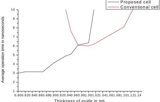
50AVERAGE50Fig: 1 show the plot between the thickness of the oxide and the average operation time in IPA devices and fig: 2 show the relationship between the transistor cell size and the average operation time in IPA devices.
IV. RESULT:MODELCORRELATION
In our correlation, the fig: 1 concluded that the average operation time is monotonically increasing with width of transistor in our proposed model whereas conventional model is non monotonically increasing with width of transistor and fig: 2 concluded that the average operation time is monotonically decreasing with width of transistor in our proposed model whereas conventional model is non monotonically decreasing with width of transistor in perpendicular to plane anisotropy of MTJ MRAM
0 .8 00 .8 20 .8 40 .8 60 .8 80 .9 00 .9 20 .9 40 .9 60 .9 81 .0 01 .0 21 .0 41 .0 61 .0 81 .1 01 .1 21 .1 4 1 2 3 4 5 6 7 8 9 1 0 A v e ra g e o p e ra ti o n t im e i n n a n o s e c o n d s
T h ic k n e s s o f o x id e in n m
[image:5.612.178.458.278.457.2]P ro p o s e d c e ll C o n v e n tio n a l c e ll
[image:5.612.173.471.519.703.2]Fig. 1 Example of an image with acceptable resolution
Fig. 1 Representation of thickness of oxide versus average operation time in PPA devices
1 .5 2 .0 2 .5 3 .0 3 .5 4 .0 4 .5 5 .0 5 .5 6 .0 6 .5 7 .0 7 .5 8 .0 8 .5 9 .0 9 .5 1 0 .01 0 .51 1 .0 1 .0 1 .5 2 .0 2 .5 3 .0 3 .5 4 .0 4 .5 5 .0 5 .5 6 .0 6 .5 7 .0 7 .5 8 .0 8 .5 9 .0 9 .5
1 0 .0 P ro p o s e d c e ll
C o n ve n tio n a l ce ll
W id th o f tra n s is to r in n m
A v e ra g e o p e ra ti o n t im e i n n a n o s e c o n d s
V. CONCLUSIONS
A new type of simple novel magnetic tunnel junction for read write performance in perpendicular to plane anisotropy is presented. We propose and computationally analysis the read-write performance of MTJ. The curve fitting of this model is more accurate to obtain good result.
VI. ACKNOWLEDGMENT
The author would like to thank to Department of S.O.S in Electronics for providing the necessary tools and software.
REFERENCES
[1] J M Pakala. Spin-transfer switching current distribution and reduction in magnetic tunneling junction-based structures. IEEE Transactions on Magnetics, 41(10):2621 – 2626, 2005.
[2] Shinji Yuasa, Taro Nagahama, Akio Fukushima, Yoshishige Suzuki, and Koji Ando. Giant room-temperature magnetoresistance in single-crystal Fe/MgO/Fe magnetic tunnel junctions. Nature Materials, 3(12):868–871, 2004.
[3] Jun Hayakawa, Shoji Ikeda, FumihiroMatsukura, Hiromasa Takahashi, and Hideo Ohno. Dependence of Giant Tunnel Magnetoresistance of Sputtered CoFeB/MgO/CoFeB Magnetic Tunnel Junctions on MgO Barrier Thickness and Annealing Temperature. Japanese Journal of Applied Physics, 44(No. 19):L587 – L589, 2005.
[4] Young Min Lee, C. Yoshida, K. Tsunoda, S. Umehara, M. Aoki, and T. Sugii. Highly scalable stt-mram with mtjs of top-pinned structure in 1t/1mtj cell. In VLSI Technology (VLSIT), 2010 Symposium on, pages 49 –50, June 2010.
[5] Jing Li, Haixin Liu, SayeefSalahuddin, and Kaushik Roy. Variation-tolerant SpinTorque Transfer (STT) MRAM array for yield enhancement. 2008 IEEE Custom Integrated Circuits Conference, (Cicc):193–196, 2008.
[6] P M Braganca, J A Katine, N C Emley, D Mauri, J R Childress, P M Rice, E Delenia, D C Ralph, and Robert A Buhrman. A Three-Terminal Approach to Developing Spin-Torque Written Magnetic Random Access Memory Cells. IEEE Transactions on Nanotechnology, 8(2):190–195, 2009.