Design & Analysis of Single Bit Sub-Threshold
Sram Using Dtmos with Traditional Sram Design
under 32nm Design
T. Vasudeva Reddy1, Dr B.K. Madhavi 2, k. Madhava Rao3 1
Research Scholar, Rayalaseema University
2
Professors, Dept. of ECE, Sridevi Women's Engg College, Hyderabad, Telangana
3
Asst Professors, Dept. of ECE, BVRIT, Narsapur, Telangana
Abstract: Due to rapid growth of the consumer electronics, there is demand of low power devices; leads to moving on to the sub threshold design logic circuits. Under the sub threshold design, the threshold design of the transistors is less than the supply
voltage, where the threshold voltage of the devices is 0.49V & supply voltage of 0.4V. The proposed research describes the
implementation of single bit sub-threshold SRAM using Dynamic Threshold MOS (DTMOS) approach. Finally a comparison is made between the novel sub threshold single bit 8T SRAM with traditional sub threshold single bit 8T SRAM in terms of leakage
power, total, rise &fall time of the delay.
Keywords: DTMOS, ST SRAM, Sub threshold regime, Schmitt trigger based SRAM,
I. INTRODUCTION
As the demanding for wide range of sophisticated, portable, energy efficient & life time of the electronics, the demand for low power electronics and increasing day by day. This leads to motivate the researchers to focus more on low power design in any of the abstraction level like circuit, device or system level modelling. Lot of research been continuously focusing in the field, still there is a uncontrollable in power under sub threshold region. Therefore this novel research is the solution for the design under sub threshold region of operation, where the circuits are operating with the supply voltage which is less than the sub threshold point of a transistor. SRAM is one of the major part in the entire design & occupies 40% of the chip area. In this research paper describes the implementation of novel Schmitt trigger based SRAM using dynamic threshold approach using high and low Vth transistors[1-3]. Functionality is estimated by read & writes operations & performance is treated power and delay analysis. This research paper describes four steps. At first, design of sub threshold Schmitt trigger based SRAM using DTNOS design and functionality is analysed by read & write operations. In the second stage, design of sub threshold 8T SRAM using traditional approach and functionality of read &write operations are analysed. The third approach deals with analysis of static or leakage power for both sch-sram & 8T SRAM. Fourth approach deals with the delay analysis by rise and fall time of both the approaches. Finally a comparison is made between power, delay and also describing the low powered applications based on minimum delay & less power consumption which is demanding the most.
II. DESIGNOFSINGLEBITSUBTHRESHOLD8TSRAMDESIGN
From the previous research & survey, it has been decided that 8T SRAM is the suitable for implementation of memory design under sub threshold region. Where the supply voltage is less than the threshold voltage of the transistors. The performance & functionality is estimated by read & write operations, power and delay analysis as showed below.
A. Schematic diagram & Read, Write operations
Fig 1.1 Circuit Diagram of 8T SRAM
he values changes in the logic with a vary in the supply voltage [1,2].Due to reduction in supply voltage, the memory cell becomes susceptible to variations and dynamic threshold voltage is due to random dopant fluctuations.Therefore the memory cell of NMOS transistors makes the memory cell less reliable during read operation. The 8T cell address this issue by separating the read and write operation. Finally the data is written and held (M1 to M6) and in the other way data is read from (M5-M6)
[3-4].The above Fig.1.4 shows is an single bit 8T SRAM model with an two transistors are acting as pull transistors, The static
noise margin can be improved in this case by separating the read and write operations. In order to write the '1' into SRAM, WL is asserted as '1', and BL is made as high and BLB is low, the value of ‘0’ is stored across 'BLB' and complement of B.
After pre-charging Bit Line (BL=BLB=1), WL is pulling one of the bit line low and others makes high. So the stability& Leakage current of 8T SRAM is greatly increased due to separation of read & write operations[4,7].The two cross-coupled inverters N1,P3 and N2, P4 are connected to back to back of N5, N6 are access transistors. In order to achieve Static Power Reduction, the two additional NMOS transistor is used here are connected to the cross-coupled inverter circuit. The gate terminal of access transistors are connected to the word line and the bit line. To select the design cell, word lines are used and read, write, operations are performed using bit lines. But internally cell holds & stores value of Q, on its node & QB on the other node. These complementary BL's are used to perform read & write operation. From the below diagram, we can consider that the circuit is symmetric, and therefore P3=P4, N1=N2, N5=N6, and N7=N8 as showed Fig 1.2
Fig 1.2 Schematic of 8T SRAM
The amount of static power and noise margin is reduced by considering the cross coupled design, which is used to reduce the Static Power. Sschematic design is implemented using 32nm, with a threshold voltage of 0.4V & suplly voltage of 0.4V,having a fixed
length and widths of transistors. These designs is simulated using synopsys circuit level design & Read & write operation are
[image:3.612.194.432.458.661.2]A. Read & write operation
Fig 1.3 Read & Write operation
During a WRITE mode, BL is pulled to VSS (writing “0” and BL bar is kept at Vdd. the source of the left inverter is reduced (BL pulled to VSS). The trip point of inverter becomes lower because of the reduced strength of PMOS transistor of inverter. The source voltage of PMOS transistor of right inverter is at Vdd enables a faster pull up for the complementary node.
B. Power Analysis
With the supply voltage of 0.4V, either of the transistor will be on at one stage, as the CMOS is operating under sub-threshold region, there is no need of changing the width of the transistors.
C. Static Power
The static mode of operation is treated under the DC supply voltage, estimating the current across the node of the input terminal. Normally under sub threshold operation, the amount of static power is increasing and dominating the dynamic power, where as in this case, using high low Vth transistor that makes the circuit to reduce the leakage power less comparatively with the other 90nm& 45nm technology. Therefore the Static power is given by 4.554nw when the circuit is under ideal operation.
Fig 1.17 static power is 4.47nw
D. Total Power
[image:4.612.83.532.434.663.2]Fig 1.18 Total power is 13.773nw
E. Delay Analysis
1) Rise time: It is the response time of the circuit under the changing the states from logic 0 to 1,Ie normally 10 to 90% of the rise
[image:5.612.180.434.330.473.2]in voltage. In this case Output Response rise time of 205 Ps, reaching from 10 to 90% of rising edge.
Fig 1.19 Rise time of 205 Ps
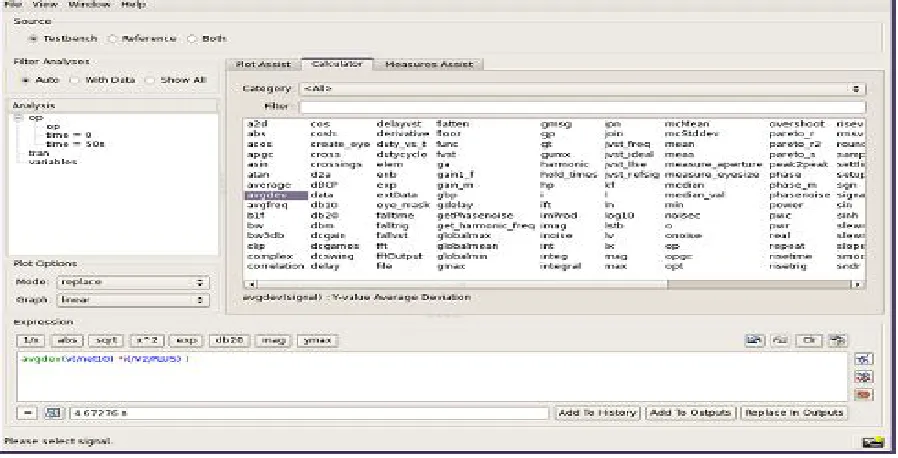
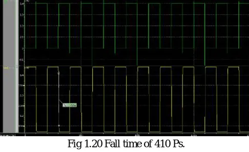
2) Fall time: It is the response time of the circuit under the changing the states from logic 1 to 0,Ie normally 90 to 10% of the fall
in voltage. In this case Output Response rise time of 410 Ps, reaching from 90 to 10% of fall edge.
Fig 1.20 Fall time of 410 Ps.
III. SUBTHRESHOLDSCHMITTTRIGGERBASEDSRAMUSINGDTMOSAPPROACH.
[image:5.612.183.426.514.663.2](DTMOS) techniques, consisting of positive feedback loop is acts as a bistable latch [6,7]. So the circuit stability can be improved [5-9]. Optimal characteristics & performance is obtained below the threshold region, with a supply voltage is less than the threshold voltage ,called sub threshold operation with a functional approach through read, write operations & Performance by power and delay is characterized A High Vth & low Vth transistor [6-8]are used to reduce the leakage power and Finally performance is estimated by static and dynamic power along with delay.
A. Design & Operation of Schmitt trigger based SRAM
Static Random Access Memory (SRAM) is a type volatile of memory that it to stores or hold the data, when power is available. A N-type transistor of N5 is added with the existing SRAM to improve the read performance and also to separate the bit lines from storage nodes. Another modification with the existing design is P3 (P-type transistor) is added with the two cross coupled inverters to break from feedback from the read operation. Therefore the read and write operations can be Separated by word lines. Therefore it leads to an asymmetric structure. [9-11].
Fig: 2.1 Sub threshold DTMOS based SRAM design
B. Read & write operation
During Write operation, the output carries ‘0’ with a input of ‘1’ at bit line. The word line has a ‘high’ and the applied input across the BL is low. This makes the value to store in the bistable latch is '1' and bit line value bar produces the output '0'. This re results in makingM3 and M4 on.
While reading, pre-charging to the bit line value to Vdd. This drives the access transistor M5 makes on & drive by Reading word line (RWL). The value stored at node Q is '0', then M7 will be on state & RBL is connected to ground, discharges through on transistors M5 & M7. Therefore the value stored at node Q is ‘0’ & QB is 1.and vice versa as showed in fig 2.2
Fig 2.3 Write operation
C. Power analysis
Power of analysis of the circuit is estimated by static or leakage Where Ptotal=Pdynamic+Pstatic+Pshort-circuit
Pactive=α CL Vdd2 Fclk
Whereα is an activity factor, CL is the load capacitance, Vdd2 is the supply voltage, Folk clock frequency static power is the product
of leakage current with supply voltage iePstatic=Vdd*Ileak.
D. Static Power
In static mode of operation is the operation under the DC supply voltage, it is estimated that, the current across the node of input terminal. In sub threshold operation, the amount of leakage power is increasing and dominating the dynamic power, but in this case, using varying the device dimensions & using high, low Vth transistor[10], makes the circuit to reduce the leakage power comparatively with the other 90nm& 45nm technologies. The Static power is given by 1.216nw when the circuit is under ideal operation. Static, total power is analyzed based on the dc input signal, where the input voltage and supply voltages are 0.4V and a threshold voltage of 0.49V. Static Power & Total power represented as showed from the following fig: 2.4. & fig: 2.5
[image:7.612.90.538.432.711.2]E. Total Power Dissipation
Fig: 2.5 Total Power of 7.256nw
F. Rise ime (tr) & Fall time (tf)
The time taken to raise the output signal from 10% to 90% of the maximum voltage is treated as rising time and represented by tr,
and 90% to 10% is treated as fall tome, represented by tf. As showed from the following Fig: 2.6 & Fig: 2.7
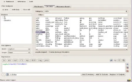
Fig: 2.6 Rise time is 112 ps
And also the total time delay of the circuits is given by the 210ps.
G. Result Analysis
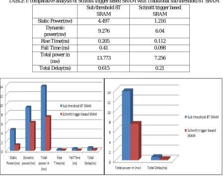
[image:9.612.82.532.167.522.2]sub threshold Schmitt trigger based SRAM is designed and compared with sub threshold 8T SRAM, in performance alsi functionality. As this design is single bit SRAM, There is no difference in read & write operations, where as it makes lot of difference in power and delay as showed in Table 1 & Fig. 2.8.
TABLE I: comparative analysis of Schmitt trigger based SRAM with Traditional sub threshold 8T SRAM Sub threshold 8T
SRAM
Schmitt trigger based SRAM
Static Power(nw) 4.497 1.216
Dynamic
power(nw) 9.276 6.04
Rise Time(ns) 0.205 0.112
Fall Time (ns) 0.41 0.098
Total power in
(nw) 13.773 7.256
Total Delay(ns) 0.615 0.21
Fig. 2.8 comparative analysis
IV. CONCLUSIONS
From the above Table 1 & Figure 2.8, by comparing the results, the static/leakage power is drastically reduced by 4.355nw, and dynamic power is reduced by 8.6883nw. Rise time & fall time is reduced by 0.093ns, 0.31ns respectively. Finally, over all power is reduced by 12.249nw and total delay is reduced by 0.415ns.From the above results, the sub threshold Schmitt trigger based SRAM is one of the prominent design under sub threshold mode of operation. This design follows the dynamic threshold Schmitt trigger operation of SRAM for low power high speed applications starting from biomedical, wireless sensor networks to processors.
REFERENCES
[1]. N. Zheng and P. Mazumder, "Modelling and Mitigation of Static Noise Margin Variation in Sub threshold SRAM Cells," in IEEE Transactions on Circuits and Systems I: Regular Papers, vol. 64, no. 10, pp. 2726-2736, Oct. 2017.doi: 10.1109/TCSI.2017.2700818.
[2]. C. B. Kushwah and S. K. Vishvakarma, "A Single-Ended With Dynamic Feedback Control 8T Sub threshold SRAM Cell," in IEEE Transactions on Very Large Scale Integration (VLSI) Systems, vol. 24, no. 1, pp. 373-377, Jan. 2016,doi: 10.1109/TVLSI.2015.2389891.
[4]. F. Moradi and J. K. Madsen, "Improved read and write margins using a novel 8T-SRAM cell," 2014 22nd International Conference on Very Large Scale Integration (VLSI-SoC), Playa del Carmen, 2014, pp. 1-5.
doi: 10.1109/VLSI-SoC.2014.7004186
[5]. Ramesh Vaddi, “Device and Circuit Design Challenges in the Digital Sub threshold Region for Ultralow-Power Applications” Indian Institute of Technology (IIT), Hindawi Publishing Corporation VLSI Design Volume 2009, Article ID 283702, doi:10.1155/2009/283702.
[6]. fariborz assaderaghi,” Dynamic threshold-voltage mosfet (DTMOS) for ultra-low voltage VLSI” IEEE transactions on electron devices, vol. 44, no. 3, March 1997.
[7]. Sayeed Ahmad, et al., “Single-ended Schmitt-trigger-based robust low-power SRAM cell by,” Journal,IEEE Transactions on Very Large Scale Integration (VLSI) Systems”,Volume24,Issue 8,Pages 2634-2642,Publisher,IEEE.
[8]. Mohsen Radfar, Mohsen et al.”Recent Sub threshold Design Techniques” Centre for Technology Infusion, La Trobe University, Hindawi Publishing Corporation Active and Passive Electronic Components Volume 2012, Article ID 926753, 11 pages doi:10.1155/2012/926753
[9]. Review of Circuit Level Leakage Minimization Techniques in CMOS VLSI Circuits by Rohit Lorenzo, ISSN: 0256-4602 (Print) 0974-5971
[10]. Low-Power VLSI Circuits and Systems by Ajit Pal, Springer India publications,2015.