Technology (IJRASET)
Ground Bouncing Noise Reduction in
Combinational Circuits
G Sudhakar1, B Venkanna2, N Bhojanna3
First -Second, RGUKT-Basar, Telangana State-504107 Third-JIET-Hyderabad, Telangana State-501510
Abstract- As technology scales into the nanometer regime ground bounce noise and noise immunity are becoming important
metric of comparable importance to leakage current, active power, delay and area for the analysis and design of complex arithmetic logic circuits. In this paper, low leakage 1bit full adder cells are proposed for mobile applications with low ground bounce noise and a novel technique has been introduced with improved staggered phase damping technique for further reduction in the peak of ground bounce noise. Noise immunity has been carefully considered since the significant threshold current of the low threshold voltage transition becomes more susceptible to noise. We introduced a new transistor resizing approach for 1bit full adder cells to determine the optimal sleep transistor size which reduce the leakage power and ground bounce noise. The simulation results depicts that the proposed design also leads to efficient 1bit full adder cells in terms of standby leakage power, active power, ground bounce noise and noise margin. We have performed simulations using Cadence
Spectre 180nm standard CMOS technology at room temperature with supply voltage of 1V.
Keywords-Ground bounce noise, Low leakage power, sleep method, Tri-mode, MTCMOS Technique.
I. INTRODUCTION
CMOS technology feature size and threshold voltage have been scaling down for decades for achieving high density and high performance. Because of this race in technology trends transistor leakage power has increased exponentially. As the feature size becomes smaller, shorter channel lengths result in increased sub-threshold leakage current through a transistor when it is in off state. Low threshold voltage also results in increasing sub threshold leakage current as transistors cannot be turned off completely. For these reasons, static power consumption, i.e., leakage power dissipation has become a significant portion of total power consumption for current and future silicon technologies. Various techniques to reduce leakage power can be reviewed from reference no [1]. In present days these techniques are implemented using MTCMOS technology in which the entire circuit is divided into multiple autonomous power/ground gating domains for effective reduction leakage power consumption[3],[4]. When an idle circuit is awaken, high currents flow through the sleep transistors. Significant voltage fluctuations occur on the power and ground distribution networks (power and ground bouncing noise). Reactivation noise has become an important reliability concern in modern Integrated Circuits [5], [6]. We propose a new approach, thus providing a choice to VLSI designers by modulating the slew rate of sleep signal resulting in low-leakage power dissipations. By applying this sleep signal at the gates of power and ground gating transistors in general the sleep transistors the required reduction in power dissipation can be achieved at a cost of lowest ground bounce noise.
II. GROUNDBOUNCINGMINIMIZATIONTECHNIQUES
To find out the efficiency of different technique and to minimize the ground bouncing, we carried out simulation on 16 bit ripple carry adder, in which we have taken a conventional full adder as base design. To show the compatibility of these technique to different environment and different level of logic we have chosen logic 1 bit Ripple Carry Adder in “180 nm” CMOS technology. We have applied these following wakeup techniques for MTCMOS 16 bit ripple Carry Full Adder.
A. Conventional one step wakeup technique
B. Tri mode technique
C. Stacking power gating technique
D. Dynamic size variation technique
Technology (IJRASET)
The block diagram of the 16 bit ripple carry adder is shown in below.
The circuit use 16 bit Full Adder circuits to add 1 bit inputs. The input string A0 – A15 AND B0 –B15 are added to give 16 bit sum S0-S15 and a carry Cout. Carry if each full adder is forwarded to the next full adder and the carry for the first full adder C0 is specially given. This entire circuit is designed with low Vth transistor for speed improvement and a sleep device of high Vth is used
to reduce the leakage as discussed in MTCMOS Technique. Simulation Setup: The simulations are carried out in “Cadence Design Environment” using “Spectre” Simulator in “180nm” CMOS Technology. The Ripple Carry Adder is designed with Low Threshold Voltage NMOS and PMOS FETs of 180nm Technology. This is used as low Vth circuit block which is connected in series with high Vth sleep transistor to minimize the leakage in sleep mode. The parasitic inductance, capacitance and resistance are taken from
the dual in line package (DIP-40) package model. The simulation parameters are:
1) NMOS High-Vt Voltage Vtnhigh = 0.5V
2) NMOS Low-Vt Voltage Vtnlow = 0.25V
3) PMOS High-Vt Voltage Vtnhigh = -0.5V
4) PMOS Low-Vt Voltage Vtnlow = -0.25V
5) Supply voltage VDD = 1.8V
6) Sleep device width = 10 µm
A. Conventional one step wakeup MTCMOS Technique
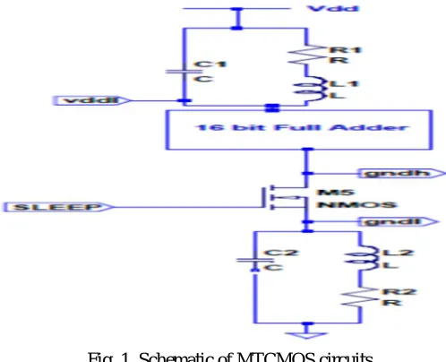
[image:3.612.178.427.497.699.2]In the schematic shown in fig.1, the sleep transistor size is taken as 10 µm. The capacitance, resistance and inductance value are taken from DIP-40 package for pin. The 16 bit ripple carry full adder used in the circuit made from conventional 28 transistors based CMOS one bit full adder.
Technology (IJRASET)
surge large amount of ground bouncing noise will be take place. Fig.2. shows the schematic diagram used for the simulation of 16 bit full adder with one step MTCMOS technology.
B. Tri-Mode Technique
In this technique, between sleep and active mode an intermediate relaxation mode is created to gradually dump the charge stored on virtual ground line to real ground distribution network during the sleep to active mode transitions. A high -|Vth| PMOS data retention
transistor (holder) is connected in parallel with the footer transistor (N1) to implement an additional PARK mode (utilized as an intermediate step between the sleep and the active modes) as illustrated in fig.2. The Holder is activated while N1 is maintained cut-off during PARK mode.
Fig.2. Schematic of Tri-mode Technique
C. Stacking Power Gating Technique
Stacking sleep transistors are used in stacking power gating technique shown in fig.3 is to reduce the magnitude of peak current and voltage glitches in power rails i.e. ground bounce noise. The strategy to implement this technique is as follows:
1) Isolating the ground for small duration during mode transition.
2) Turning ON the M2 transistor in linear region instead of saturation region to decrease the current surge. During sleep to active mode transition, transistor M1 is turned ON and transistor M2 is turned ON after a small duration of time (ΔT). The logic circuit is isolated from the ground for a short duration as the transistor M2 is turned OFF. During this duration, the ground bounce noise can be greatly reduced.
Technology (IJRASET)
D. Slow rising wakeup signal MTCMOS
By applying a slowly rising wakeup signal we can control the rate of change of current passing through the sleep device. So we can reduce the ground bouncing to the desired value by increasing the rise time of the signal. The slow rising wakeup signal can be achieved by a two inverter chain as shown in fig.4. By increasing the length of the P2 transistor we can achieve the required signal.
Fig.4. Schematic of Slow rising wakeup signal MTCMOS
III. SIMULATIONRESULTS
In this section the ground bouncing waveform for 16 bit ripple carry adder are shown for each of the technique used to minimize the ground bouncing.
A. Simulation result for one step wakeup conventional MTCMOS Technique
Fig.5. is the simulation result of the schematic from fig.1. The result reveals that the maximum peak of the ground bounce noise induced is nearly 356.39 mV and the maximum peak of current surge is 13.69mA.
Technology (IJRASET)
B. Simulation result for Tri-Mode Technique
Fig.6. is the simulation result of the schematic from fig.2. The result reveals that the maximum peak of the ground bounce noise induced is nearly 79.13 mV and the maximum peak
of current surge is 11.86 mA.
Fig.6.Tri-mode Technique simulation result
C. Simulation result for Stacking power gating Technique
Fig.7. is the simulation result of the schematic from fig.3. The result reveals that the maximum peak of the ground bounce noise induced is nearly 92.66 mV and the maximum peak of current surge is 0.932 mA.
Fig.7. Simulation result for stacking power gating technique
D. Simulation result for slow rising wakeup signal MTCMOS Technique
Fig.8. is the simulation result of the schematic from fig.4. The result reveals that the maximum peak of the ground bounce noise induced is nearly 28.48 mV and the maximum peak of current surge is 0.63 mA. As we can see from the fig.4.that even after the ground bounce is nearly nullified the wakeup signal is still rising to reach VDD. So the time taken for the sleep device to be
Technology (IJRASET)
Fig.8. Simulation result for slow rising signal Technique
E. Comparison Result of Different Technique
To minimize the ground bouncing, different techniques are proposed. All these technique are successful in minimizing the ground bouncing. In this section we have compared these techniques in terms of the amount of ground bounce minimization, wakeup delay, area overhead caused by the extra circuitry to implement these techniques and the leakage power.
IV. GROUND BOUNCING
The amount of ground bouncing is tabulated in table.1.for 16 Bit Full Adder. All the results taken are from cadence tool at 180nm technology.
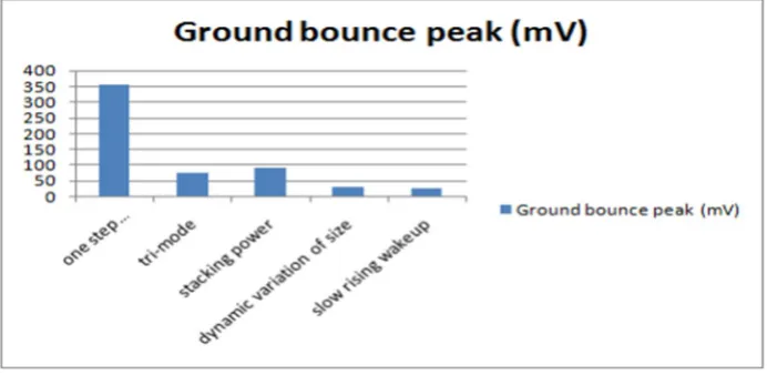
Table 1. Comparison of GBN reduction technique for ground bounce Technique used Ground bounce peak (mV) Reduction percentage MTCMOS Technology 356.39
Tri-mode 79.13 77.79%
Stacking power gating 92.66 74%
Dynamic Variation of sizes 31.18 91.2% Slow rising wake up signal 28.48 92 %
[image:7.612.134.480.533.702.2]Technology (IJRASET)
V. CONCLUSIONS
MTCMOS Power Gating is a very effective technique for low power VLSI design. But this technique suffers from ground bouncing noise during sleep to active mode transition. To minimize the ground bouncing noise, different techniques are applied on a 16-bit Ripple carry Adder in 180 nm CMOS Technology. We have investigated the ground bounce caused by large charge and discharge currents through a sleep transistor during the mode transition of a power-gating structure. In the proposed slow rising wakeup technique, the primary motive for the technique is to reduce ground bouncing which is controlled by controlling the rate of change of current. This is achieved in the proposed technique by applying a wake signal having long rise time. The wakeup signal is applied to an inverter chain whose output is applied to the sleep device. By applying slow rising wakeup signal as power gating solution we are able to suppress the ground bouncing amplitude by 92%. The comparison of the proposed technique with other ground bounce reduction technique like Tri–mode technique, stacking power technique and dynamic variation of size of sleep device have done on different parameter like amount of ground bounce noise reduced, amount of current surge, average power, wakeup delay and area overhead. The slow rising wakeup signal MTCMOS Technique has reduced the amplitude of ground bounce by maximum percentage of 92% in comparison to other techniques.
REFERENCES
[1] Md. Asif Jahangir Chowdhury, Md. Shahriar Rizwan, and M. S. Islam, “An Efficient VLSI Design Approach To Reduce Static power using Variable Body
Biasing,” in World Academy Of Science, Engineering and Technology 64 2012.
[2] S. Kim, C.J. Choi, D. Jeong, S. V. Kosonocky and S. Park, “Reducing Ground-Bounce Noise and Stabilizing the Data-Retention Voltage of Power-Gating
Structures,” IEEE Transactions on Electron Device, VOL. 55, NO. 1, pp. 197-205, January 2008.
[3] H. Jiao and V. Kursun, “Ground Bouncing Noise Suppression Techniques for MTCMOS Circuits,” IEEE 1st Internatioal Symposium on Quality Electronic
Design-Asia, pp. 64-70, April 2009.
[4] P. Heydari and M. Pedram, “Ground Bounce in Digital VLSI circuits,” IEEE Transactions on Very Large Scale Integration (VLSI) Systems, Vol. 11, No. 2,
pp. 180-185, April 2003.
[5] H. Jiao and V. Kursun, “Reactivation Noise Suppression with Sleep Signal Slew Rate Modulation in MTCMOS Circuits,” IEEE Transaction on Very Large
Scale Integration (VLSI), VOL. 21, NO. 3, pp. 533-545, January 2013.
[6] R. Bhanuprakash, M. Pattanaik, S. S. Rajput and K. Mazumdar, “Analysis and Reduction of Ground Bounce Noise and Leakage Current During Mode
Transition of Stacking Power Gating Logic Circuits,” IEEE Computer Society Annual Symposium on VLSI, VOL 41, pp. 37-43, August 2009.
[7] M. H. Chowdhury, J. Gjanci, and P. Khaled, “Controlling Ground Bounce Noise in Power Gating Scheme for System-on-a-Chip,” IEEE Computer Society
Annual Symposium on VLSI, VOL 37, pp. 437-440, December 2008.
[8] M. Pattanaik, V. L. Varaprasad and F. R. Khan, “Ground Bounce Noise Reduction of Low leakage 1-bit Nano-CMOS based Full Adder Cells for Mobile
Applications,” IEEE International conference on electronics device, system and application, pp. 31-36, 2010.
[9] S. Kim, S. V. Kosonocky, D. R. Knebel, K. Stawiasz, and M. C. Papaefthymiou, “A multi-mode power gating structure for low-voltage deep-submicron
CMOSICs,” IEEE Transaction on Circuits Sysems, vol. 54, no. 7, pp. 586–590, July 2007.
[10] K. Roy, S. Mukhopadhyay and H. M. Meimand, “Leakage Current Mechanisms and Leakage Reduction Techniques in Deep- Submicrometer CMOS circuits”,
IEEE International Symposiumon on Low Power Electronics Designs, vol. 41, pp. 305– 327, February 2003.
[11] Z. Liu and V. Kursun, “Characterization of wake-up delay versus sleep mode power consumption and sleep/active mode transition energy overhead tradeoffs