N A N O E X P R E S S
Open Access
Array of solid-state dye-sensitized solar cells with
micropatterned TiO
2
nanoparticles for a
high-voltage power source
Seong-Min Cho
1, Hea-Lim Park
1, Min-Hoi Kim
2, Se-Um Kim
1and Sin-Doo Lee
1*Abstract
We demonstrate an array of solid-state dye-sensitized solar cells (SS-DSSCs) for a high-voltage power source based on micropatterned titanium dioxide nanoparticles (TNPs) as photoanodes connected in series. The underlying concept of patterning the TNP of a few micrometers thick lies on the combination of the lift-off process of transfer-printed patterns of a sacrificial layer and the soft-cure treatment of the TNP for fixation. This sacrificial layer approach allows for high pattern fidelity and stability, and it enables to construct stable, micrometer-thick, and
contamination-free TNP patterns for developing the SS-DSSC array for miniature high-voltage applications. The array of 20 SS-DSSCs integrated in series is found to show a voltage output of around 7 V.
Keywords:Titanium dioxide nanoparticle; Micropatterning; Solid-state dye-sensitized solar cell; High-voltage source
PACS:81.16.Rf; 85.40.Hp; 84.60.Jt
Background
Dye-sensitized solar cells (DSSCs) with mesoporous ti-tanium dioxide (TiO2) nanoparticles (TNPs) have been considered as a promising alternative to conventional in-organic solar cells due to their relatively high power con-version efficiencies and low production cost [1]. So far, much effort has been made toward the enhancement of the power conversion efficiency of the DSSCs [2-4]. To-gether with the improvement of the power conversion efficiency, the generation of high output voltage is one of the critical issues for practical applications. The issue of the high voltage generation of the DSSCs has been addressed only in a unit cell producing limited output voltages of around 1 V [5-7], which is far below the volt-ages required for most practical devices, for example, around 4 V for mobile phones. Thus, the integration of DSSCs needs to be pursued for high-voltage sources. Owing to the excellent electron transport characteris-tics, stability, and appropriate conduction band position, a TNP layer is promising for use as a photoanode in the DSSC [8]. Therefore, for the integration of a DSSC
array, a reliable patterning technique of the TNP layer should be developed.
In patterning the TNP, several methods such as solvent-assisted soft lithography [9], micromolding technique in capillaries [10], and imprint lithography [11] have been typically employed, but they involve the difficulty of pat-terning multiple stacks of the TNP and eliminating the re-sidual layer. In other words, these patterning methods are not applicable for constructing relatively thick (a few micrometers) and stable TNP patterns demanded for sufficiently high absorption of light in the DSSCs [12]. Moreover, the DSSCs with liquid electrolytes encounter confinement problem, leakage, and evaporation of the liquid in the integration into the array. Therefore, it is extremely important to develop a versatile method of patterning a few-micrometer-thick TNP layer for fabri-cating an array of solid-state dye-sensitized solar cells (SS-DSSCs).
In this work, we demonstrate an array of SS-DSSCs for a high-voltage power source using micropatterned TNP as photoanodes connected in series. The basic con-cept relies primarily on a chemically compatible lift-off process of a fluorous sacrificial layer which has the com-plementary patterns of the TNP of a few micrometers thick on a substrate. This sacrificial layer approach * Correspondence:[email protected]
1
School of Electrical Engineering, Seoul National University, Kwanak, PO Box 34, Seoul 151-600, South Korea
Full list of author information is available at the end of the article
allows for high pattern fidelity and stability, and it leads directly to stable, micrometer-thick, and contamination-free TNP patterns for developing the SS-DSSC array for miniature high-voltage applications.
Methods
Fabrication of TNP patterns
In preparing photoanodes connected in series for a high-voltage DSSC array, micropatterns of the TNP were constructed on a pre-patterned fluorine-doped tin oxide (FTO) glass. An array of 20 FTO electrodes, where each
electrode has a width of 500 μm and a gap of 500 μm
between two adjacent electrodes, was prepared using photolithography and a dry etching process. A glass sub-strate with pre-patterned FTO was cleaned with acetone, deionized water, and ethanol in sequence and dried with nitrogen flow. The cleaned substrate was then dried at 90°C in a vacuum oven for 10 min to remove any re-sidual water and subsequently treated with ultraviolet ozone for 5 min. In order to improve the adhesion and the mechanical strength of the TNP layer [13], the treated FTO glass was soaked in an aqueous solution of 40 mM TiCl4at 70°C for 30 min. The FTO glass was then cleaned in the same way described above.
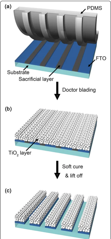
Figure 1 shows the schematic diagram illustrating the fabrication of a patterned TNP layer on the FTO glass. The entire fabrication processes of patterning TNP are as follows: An elastomer stamp with patterns, complemen-tary to desired TNP patterns, was made of poly-(dimethyl-siloxane) (PDMS). For fabricating complementary patterns of a sacrificial layer (SL) on the FTO glass, a fluorous
poly-mer (3 M Novec™EGC-1700, 3 M Novec, Manassas, VA,
USA) dissolved in a highly fluorous solvent (3 M Novec™ HFE-7100) was dip-coated on the prepared PDMS stamp. Figure 1a shows the transfer printing process of the com-plementary patterns of the SL on the PDMS stamp onto the FTO glass. Note that no additional pressure or heat is required during transfer printing due to the lower surface energy of the PDMS stamp than that of the FTO glass [14]. Ti-Nanoxide T (Solaronix SA, Aubonne, VD, Switzerland) paste was subsequently prepared on the SL-patterned FTO glass to form a TNP layer using a doctor-blading technique, as shown in Figure 1b. The TNP film was soft-cured at 50°C for 3 min for the fixation of the TNPs to ensure stability during the following lift-off process. In the soft-cure treatment, the duration of heat-ing plays a critical role in patternheat-ing the TNP layer of a few micrometers thick; the TNP layer should be suffi-ciently soft for the application of the lift-off process but structurally strong enough to prevent the collapse of the TNP stacks during the lift-off process. Figure 1c illustrates the SL layer which was lifted-off in a fluorous solvent, leaving only the line patterns of the TNP layer on the FTO active regions. Note that the fluorous solvent is
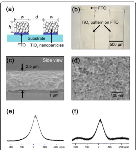
[image:2.595.304.539.88.593.2]chemically inert to most organic and inorganic materials [14,15]. The patterned TNP layer was annealed at 80°C for 2 h and then at 450°C for 30 min. As shown in Figure 2a, the TNP pattern whose width (w) and distance (d) were 500 μm, respectively, was well defined according to the
PDMS pattern. In principle, the TNP patterns can be achieved down to a submicrometer scale depending on the dimension of the elastomer stamp patterns or the SL patterns [11].
Preparation of a DSSC array
Each patterned TNP used as an individual photoanode for a unit cell was connected in series for a high-voltage DSSC array. The patterned TNP layer was immersed in a solution of 3 mM Z907 dye (Solaronix SA) dissolved in a 1:1 mixture of acetonitrile andtert-butyl alcohol for 24 h. The dye-coated TNP layer was simply washed with acetonitrile. For the solid-state hole transport material (HTM), spiro-OMeTAD (American Dye Source, Inc., Baie D'Urfé, Quebec, Canada) dissolved in chlorobenzene was mixed with a lithium bis(trifluoromethylsulfonyl)imide salt ionic dopant dissolved in acetonitrile. The solution was placed on the whole TNP-patterned FTO glass, and the pores in the TNP layer were filled with the solution by ca-pillary action for 1 min. The TNP-patterned FTO glass was then spun at the rate of 2,000 rpm. For the preparation of a cathode, Au of 100 nm thick was thermally deposited at
the rate of 1 Å/s through a shadow mask to connect 20 cells in series. The array of 20 DSSCs connected in series has a total active area of 1.4 cm2.
Characterization methods
An optical microscope and a field emission scanning electron microscope (FE-SEM; SU-70, Hitachi, Ltd., Chiyoda, Tokyo, Japan) were used for taking the images of the patterned TNP layer. In order to examine the exis-tence of any residual fluorous solvent in the patterned TNP layer which may deteriorate the photovoltaic performance of the SS-DSSCs, solid fluorine-nuclear magnetic resonance (19F-NMR) spectra were measured with a Bruker AVANCE II (500 MHz) spectrometer (Bruker, Billerica, MA, USA) with a 2.5-mm probe at the spin rate of 20 kHz. A current–voltage curve was obtained using a source measure unit (model 2400, Keithley Instruments Inc., Cleveland, OH, USA) under the il-lumination of a solar simulator with air mass 1.5 glo-bal (AM 1.5 G) filters at 100 mW/cm2. The light intensity of the solar simulator was calibrated with a standard silicon diode.
Results and discussion
The optical microscopic image of the TNP patterns in the FTO regions on the substrate is shown in Figure 2b where TNP patterns isolated from the neighboring pat-terns were clearly seen. Each isolated TNP pattern, which is 500μm wide and 14 mm long in the interval of 500μm, represents an individual photoanode for a unit cell in the SS-DSSC array [14,15]. Figure 2c shows the FE-SEM image of the cross-sectional TNP pattern. Ac-cording to the FE-SEM image, each TNP pattern was about 2.5 μm thick. This is a typical thickness of the TNP photoanode for a whole SS-DSSC [12]. Moreover, as shown in Figure 2d, the TNPs were highly packed in the multistacks of a few micrometers, and the surface roughness was about a few tens of nanometers. It should be noted that our micropatterning method based on the SL lift-off process is very simple and effective to produce a wide range of the TNP patterns by varying the thickness of the doctor-bladed TNP layer and the dimension of the SL patterns transfer-printed by the PDMS stamp.
For lifting-off the SL, the FTO substrate with the TNP patterns was exposed to a fluorous solvent. From the mea-surements of the19F-NMR spectrum of the TNP sample treated by a fluorous solvent, no extra peak was observed when compared to an empty rotor, as shown in Figure 2f. This tells us that no remnant solvent exists after annealing the TNP sample at 450°C, and thus, the SL lift-off process is contamination free for patterning the multistacks of TNPs in the fabrication of the array of the SS-DSSCs.
[image:3.595.56.291.87.347.2]Figure 3 shows the array configuration of three DSSCs connected in series together with a cross-sectional view
Figure 2Schematic diagram of TiO2pattern, images taken with optical microscopy and FE-SEM, and solid19F-NMR spectra. (a)Dimension of a TiO2pattern: the width (w), the distance (d), and
the height (h) are 500, 500, and 2.5μm, respectively.(b)The optical microscopic image of the TNP patterns on the FTO glass.(c)The FE-SEM image of the cross section of the patterned TNP layer of 2.5μm thick.(d)The high-resolution FE-SEM image of the highly packed TNPs. The solid19F-NMR spectra of(e)an empty rotor and
of a unit cell consisting of the FTO layer, TNPs with dyes, HTM, and Au electrode. For the series connection, the Au cathode in a certain unit cell is connected to the patterned FTO layer in the adjacent unit cell. In describ-ing the charge flow in the unit DSSC, when the incom-ing light is absorbed by the photosensitizincom-ing dyes, the electrons are injected into the conduction band of the TNPs and move toward the FTO electrode. Meanwhile, the oxidized dyes are reduced by the HTM which is re-generated at the Au cathode [16].
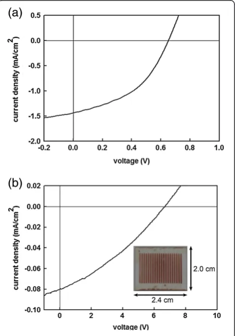
Figure 4a,b shows the current–voltage curve of a single SS-DSSC and that of the array consisting of 20 SS-DSSCs measured under the illumination of simulated AM 1.5 G solar light (100 mW/cm2). For a single cell, the values of the short-circuit current density (Jsc), open-circuit voltage (Voc), and fill factor (FF) are found to be 1.44 mA/cm2, 0.65 V, and 0.44, respectively. The power conversion effi-ciency (PCE) is about 0.41%. For the array of 20 cells, the values of Jsc,Voc, and FF are 0.08 mA/cm2, 6.68 V, and 0.32, respectively, and the resultant PCE is 0.17%. The series resistance (Rs) of the single cell and that of the array of 20 cells derived from the inverse slopes of the plots (or dV/dJ when J= 0) [17] are 1.52 × 10² and 5.45 × 10⁴ Ω cm2, respectively. Note that the value of Voc(6.68 V) for the array of 20 cells is quite smaller than the value (13 V) corresponding to the simple addition ofVocfor a single cell. This is partially attributed to the non-ideal series connection due to the non-patterned HTM. In addition, the alignment between FTO and the patterned TNP layer may not be perfect, and thus, the active regions become reduced. A better alignment would give a higher voltage. The values of the FF and the PCE also become low, due to the increase in the leakage current around the sides of the unit cells and the large value ofRs asso-ciated with more FTO-TNP interfaces and HTM-metal junctions. The photovoltaic performance can be im-proved, in principle, by tailoring the materials them-selves, patterning the solid-state electrolyte, aligning accurately the FTO and the TNP patterns, and optimi-zing device parameters and geometries. It should be em-phasized that our work provides a new route to the
construction of TNP patterns of a few micrometers thick in a simple and reliable way.
Conclusions
We presented how a functional layer of the nanoparti-cles can be patterned for use in hybrid electronic and optoelectronic devices in a simple, cost-effective, and
[image:4.595.307.539.348.680.2]Figure 3Schematic diagram showing an array of three SS-DSSCs connected in series and a unit cell.
Figure 4Current–voltage curves of SS-DSSCs.Current–voltage curves of(a)a single cell and(b)an array of 20 SS-DSSCs measured under the illumination of a simulated AM 1.5 G solar light (100 mW/cm2).
contamination-free way. The underlying concept comes from the lift-off process of the transfer-printed patterns of a fluorous sacrificial layer and the soft-cure treatment of the nanoparticles for fixation. As an example, an array of the SS-DSSCs with a micropatterned TNP layer of several micrometers thick was demonstrated for high-voltage source applications. The array of 20 SS-DSSCs connected in series showed an open-circuit voltage ex-ceeding 6 V. It is concluded that the micropatterning ap-proach presented here will be applicable for a wide range of diverse nanoparticles to be employed in optical, electronic, and sensing devices.
Abbreviations
AM 1.5 G:Air mass 1.5 global; DSSC: Dye-sensitized solar cell; FE-SEM: Field emission scanning electron microscope; FF: Fill factor;19F-NMR:
Fluorine-nuclear magnetic resonance; FTO: Fluorine-doped tin oxide; HTM: Hole transport material;Jsc: Short-circuit current density; PCE: Power conversion
efficiency; PDMS: Poly-(dimethylsiloxane);Rs: Series resistance; SL: Sacrificial
layer; SS-DSSC: Solid-state dye-sensitized solar cell; TiO2: Titanium dioxide;
TNP: Titanium dioxide nanoparticles;Voc: Open-circuit voltage.
Competing interests
The authors declare that they have no competing interests.
Authors’contributions
SMC, MHK, and SDL conceived and designed the experiment. SMC and SUK fabricated the TNP patterns. SMC and HLP fabricated the DSSC array, performed the electrical and optical measurements, analyzed the data, and interpreted the results. HLP, MHK, and SDL wrote the paper. All authors read and approved the final manuscript.
Acknowledgements
This work was supported by the National Research Foundation of Korea under the Ministry of Education, Science and Technology of Korea through the grant 2011–0028422.
Author details
1
School of Electrical Engineering, Seoul National University, Kwanak, PO Box 34, Seoul 151-600, South Korea.2School of Global Convergence Studies,
Hanbat National University, 125 Dongseodaero, Yuseong-gu, Daejeon 305-719, South Korea.
Received: 10 July 2013 Accepted: 6 November 2013 Published: 20 November 2013
References
1. O'Regan B, Grätzel M:A low-cost, high-efficiency solar-cell based on dye-sensitized colloidal TiO2films.Nature1991,353:737–740.
2. Chen DH, Huang FZ, Cheng YB, Caruso RA:Mesoporous anatase TiO2 beads with high surface areas and controllable pore sizes: a superior candidate for high-performance dye-sensitized solar cells.Adv Mater
2009,21:2206–2210.
3. Hara K, Sato T, Katoh R, Furube A, Yoshihara T, Murai M, Kurashige M, Ito S, Shinpo A, Suga S, Arakawa H:Novel conjugated organic dyes for efficient dye-sensitized solar cells.Adv Funct Mater2005,15:246–252.
4. Meng QB, Takahashi K, Zhang XT, Sutanto I, Rao TN, Sato O, Fujishima A, Watanabe H, Nakamori T, Uragami M:Fabrication of an efficient solid-state dye-sensitized solar cell.Langmuir2003,19:3572–3574.
5. Bach U, Lupo D, Comte P, Moser JE, Weissortel F, Salbeck J, Spreitzer H, Grätzel M:Solid-state dye-sensitized mesoporous TiO2solar cells with high photon-to-electron conversion efficiencies.Nature1998,
395:583–585.
6. Chen P, Yum JH, De Angelis F, Mosconi E, Fantacci S, Moon SJ, Baker RH, Ko J, Nazeeruddin MK, Grätzel M:High open-circuit voltage solid-state dye-sensitized solar cells with organic dye.Nano Lett2009,9:2487–2492. 7. Yella A, Lee HW, Tsao HN, Yi CY, Chandiran AK, Nazeeruddin MK, Diau EWG,
Yeh CY, Zakeeruddin SM, Grätzel M:Porphyrin-sensitized solar cells with
cobalt (II/III)-based redox electrolyte exceed 12 percent efficiency.
Science2011,334:629–634.
8. Niggemann M, Graf W, Gombert A:Realization of ultrahigh photovoltages with organic photovoltaic nanomodules.Adv Mater2008,20:4055–4060. 9. Shi G, Lu N, Gao L, Xu H, Yang B, Li Y, Wu Y, Chi L:Fabrication of TiO2
arrays using solvent-assisted soft lithography.Langmuir2009,
25:9639–9643.
10. Khan SU, Elshof JE:Patterning titania with the conventional and modified micromolding in capillaries technique from sol–gel and dispersion solutions.Sci Technol Adv Mater2012,13:025002.
11. Kim J, Koh JK, Kim B, Kim JH, Kim E:Nanopatterning of mesoporous inorganic oxide films for efficient light harvesting of dye-sensitized solar cells.Angewandte Chemie2012,51:6864–6869.
12. Ding IK, Tetreault N, Brillet J, Hardin BE, Smith EH, Rosenthal SJ, Sauvage F, Grätzel M, McGehee MD:Pore-filling of spiro-OMeTAD in solid-state dye sensitized solar cells: quantification, mechanism, and consequences for device performance.Adv Funct Mater2009,19:2431–2436.
13. Ito S, Murakami TN, Comte P, Liska P, Grätzel C, Nazeeruddin MK, Grätzel M:
Fabrication of thin film dye sensitized solar cells with solar to electric power conversion efficiency over 10%.Thin Solid Films2008,
516:4613–4619.
14. Advanced materials, Choi W, Kim M-H, Na Y-J, Lee S-D:Complementary transfer-assisted patterning of high-resolution heterogeneous elements on plastic substrates for flexible electronics.Org Electron2010,
11:2026–2031.
15. Choi W, Kim MH, Lee SD:Chemically compatible sacrificial layer-assisted lift-off patterning method for fabrication of organic light-emitting dis-plays.Jpn J Appl Phys2011,50:080219.
16. Hardin BE, Snaith HJ, McGehee MD:The renaissance of dye-sensitized solar cells.Nat Photonics2012,6:162–169.
17. Zhang CF, Zhang JC, Hao Y, Lin ZH, Zhu CX:A simple and efficient solar cell parameter extraction method from a single current–voltage curve.
J Appl Phys2011,110:064504.
doi:10.1186/1556-276X-8-491
Cite this article as:Choet al.:Array of solid-state dye-sensitized solar
cells with micropatterned TiO2nanoparticles for a
high-voltage power source.Nanoscale Research Letters20138:491.
Submit your manuscript to a
journal and benefi t from:
7 Convenient online submission
7 Rigorous peer review
7 Immediate publication on acceptance
7 Open access: articles freely available online
7 High visibility within the fi eld
7 Retaining the copyright to your article