N A N O E X P R E S S
Magnetic Behavior of Surface Nanostructured 50-nm Nickel
Thin Films
Prashant Kumar
Received: 7 May 2010 / Accepted: 30 June 2010 / Published online: 21 July 2010 ÓThe Author(s) 2010. This article is published with open access at Springerlink.com
Abstract Thermally evaporated 50-nm nickel thin films coated on borosilicate glass substrates were nanostructured by excimer laser (0.5 J/cm2, single shot), DC electric field (up to 2 kV/cm) and trench-template assisted technique. Nanoparticle arrays (anisotropic growth features) have been observed to form in the direction of electric field for DC electric field treatment case and ruptured thin film (isotropic growth features) growth for excimer laser treat-ment case. For trench-template assisted technique; nano-wires (70–150 nm diameters) have grown along the length of trench template. Coercive field and saturation magneti-zation are observed to be strongly dependent on nano-structuring techniques.
Keywords Magnetic nanostructures
Magnetic propertiesSurface treatment
Introduction
Fabrication of nanostructured nickel thin films is of importance due to its potential applications in diverse fields such as high density recording media, ferrofluid technol-ogy, spin valves, magnetic resonance imaging, magnetoc-aloric refrigeration [1–3] and as catalyst for the growth of carbon nanotubes [4]. The ability to control and manipulate the physical and chemical properties of materials is one of the challenges in nanotechnology. Surface nanostruc-turing provides a competitive platform for such pursuits.
Moreover, thin films coated onto borosilicate glass sub-strate are amorphous in nature. It has to be crystallized employing some high energy density trigger to function-alize it. Excimer laser nanostructuring of surfaces is well documented for nanostructuring [5–13]. However, electric field-induced nanostructuring technique as a field of research is currently being explored for its possible appli-cations [14–19]. Further, nickel nanowires or nanorods have received considerable attention for their wide range of potential applications in sensors and others [20–26]. Use of trench templates is one of the few techniques for the growth of nanowires.
Magnetic properties of nanostructured materials [27–30] in general and nanoparticle arrays [31,32] in particular have been active areas of research. Nanoparticle size, shape and more importantly its separation are important in determin-ing the magnetic interaction among nanocrystals. Coercive field of the material in general has to do with the size of grain and the grain separation. While on the other hand, technical saturation magnetic moment value has to do with the density of the material, the total net material volume on the substrate; apart from the magnetic anisotropy induced. Magnetization dynamics in arrays of strongly interacting magnetic nanocrystals have been carried out [33].
Current authors have carried out detailed experimental research on non-lithographic techniques [34] for surface nanostructuring which includes excimer laser nanostruc-turing [35], electric field-induced nanostructuring [35–37] and trench-template assisted in situ fabrication of nano-wires [38]. These nanostructuring techniques when employed to 50-nm nickel thin films give rise to different morphology which itself is an independent pursuit of research. However, these different morphologies for nickel thin films are expected to yield different magnetization and magnetization reversal behaviors.
P. Kumar (&)
Chemistry and Physics of Materials Unit (CPMU), Jawaharlal Nehru Centre for Advanced Scientific Research, Jakkur P. O., Bangalore 560064, India
The present paper reports the modification of the surface morphology of 50-nm nickel thin films by excimer laser, DC electric field and trench-template assisted technique. Room temperature magnetic properties of the modified nanostructured nickel thin film surfaces have also been carried out.
Materials and Methods
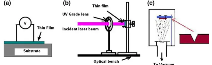
Nickel thin films of thickness 50 nm were deposited onto borosilicate glass (BSG) substrates using resistive thermal evaporation at ambient temperature in a high vacuum chamber at the base pressure of 1910-6mbar and at a rate of deposition of 0.1–0.4 nm/s. The BSG substrates were cleaned ultrasonically in acetone, isopropyl alcohol and distilled water for 15 min each and after that dried in an oven at 180°C for 20 min. Thermal evaporation was carried out with pure nickel wires (99.998%, 0.5 mm diameter, Sigma–Aldrich) placed in a tungsten spiral source that was located at a distance of 8–10 cm from the substrates. Film thickness was measured in situ using a quartz crystal thickness monitor and confirmedex situby a surface pro-filometer (XP-1 of Ambios Technology, USA). The use of an electric field, an excimer laser and trench-template assisted technique has been utilized for the nanostructuring of 50-nm nickel thin films. The methods of nanostructuring by these three techniques are described as follows. Electric Field-Induced Nanostructuring
Electric field-induced nanostructuring was carried out on samples of nickel thin films coated on BSG substrates; all cut from the same piece of original thin film [37,38]. Thin films were placed in an electric field (up to 2 kV/cm) using a DC power supply (APLABS India, model H 10003) which connected to the electrode pins having a tip area of 0.1 mm2, and the electrode separation was varied in the range of 2–5 mm. All the experiments were carried out in air medium at room temperature. Nickel thin film coated on the BSG substrate was clamped in horizontal orientation and electrode pins was kept vertically standing on the thin
film as shown in Fig.1a. Electrode pins were brought in contact from up, and it was gently made standing in contact with the film such that thin film surfaces were not scratched.
Excimer Laser-Induced Nanostructuring
The 50-nm nickel thin film evaporated on a borosilicate glass (BSG) substrate was clamped in the vertical plane where the excimer laser with a rectangular cross-section (8 mm927 mm) was exposed to it. For the nanostruc-turing, the excimer laser was not focused at all. Lambda Physik KrF (248 nm) excimer laser source was used with optimized laser fluence value (0.5 J/cm2) for single-shot irradiation to nanostructure thin film surfaces as shown in Fig.1b. Excimer laser nanostructuring has been carried out in air at room temperature conditions [35].
Trench-Template Assisted Technique for the Growth of Nanowires
For trench-template assisted in situ growth of nanowires, v-groove trenches of various diameters and depths were first scribed using electronically controlled diamond scriber onto BSG substrates that are already spin coated by maleic acid. Variation of physical loads (in terms of 10 s of grams) on the diamond scriber gives rise to the variation of diameter and depth of the trenches so formed. Thereafter, such trench templated substrates were used in inverted orientation for metallic nickel thin film growth in resistive thermal evaporation system as shown in Fig.1c. After the nickel deposition, maleic acid was then washed off in water, and thus trench to trench isolation was achieved. The details of the technique have been reported elsewhere [38].
Characterizations
Atomic force microscopy (AFM) was employed for the morphological testing. AFM imaging was made at room temperature using dynamic force mode of a multimode imaging unit (SPA-400, Seiko Instruments Inc., Chiba,
Fig. 1 Schematic of the nickel
[image:2.595.198.549.603.712.2]Japan) equipped with a controller (SPI3800N, Seiko Instruments Inc.). Samples were placed on top of the pie-zoelectric scanner, the maximum xy imaging range of which is approximately 20l and scanned at a scanning frequency of 0.5–1 Hz using a beam-shaped Si cantilever with a quoted spring constant of 12 N/m at a driving fre-quency of 136 kHz.
Magnetic measurements were taken in vibrating sample magnetometer (VSM) (Lakeshore cryotronics) at room temperature and at ambient pressure conditions. Noise floor value was 1910-7 emu at 10 s/point data collection speed, and it was 7.5910-7emu noise floor at 0.1 s/point data collection speed. Stability of the value of magnetic moment was observed to be±0.05% per day which can be considered fare for sensitive experimentation. Very small step sizes in magnetic fields were adopted for magnetiza-tion of samples. Between the magnetic field steps, long time was given to gather the data points for magnetic moments, and statistical average value at that particular magnetic field was registered by the machine.
For each sample, small nickel sphere standard was used to calibrate the VSM machine. Each time, the Teflon stick holding the thin film sample was saddled, and the direction of the stick was fixed where the magnetic moment was observed to be maximum. All experiments were carried out in nighttime to minimize noises, and the VSM was situated in a clean room at ground floor far from any noises. Sub-strate contribution to magnetic moments (m) was sub-tracted from the magnetic moments of substrate plus thin film. This subtraction was carried out by first determining the slope of the m vs. H curve as obtained for the thin film plus substrate. Then, a straight line equation (m-m1)= slope (H-H1) was written, and magnetic moment values corresponding to each magnetic field values were obtained from this equation. These values of magnetic moments due to substrate diamagnetic behavior were written in a col-umn, and then this column values were then subtracted from the column of data for original magnetic moment values for thin film plus substrate. Thus, the magnetic moment values achieved represent the thin film material magnetic moment only.
Results
Microstructure
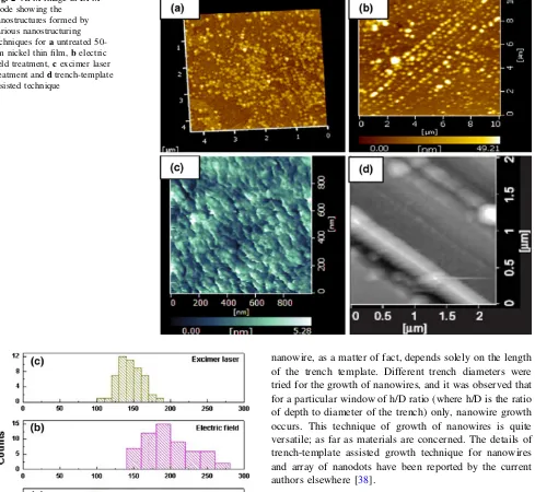
Adhesion of nickel on BSG being poor; room temperature-deposited thin films show granular kind of nanostructures. Fifty-nanometer nickel thin film shows isolated grains as shown in Fig.2a where grain sizes were found in the range of 60–130 nm as shown in grain size distribution plot in
Fig.3a. Different nanostructuring techniques have yielded different kinds of morphological features.
(a) Electric Field-Induced Nanostructuring
With the progressive increase of electric field value applied on 50-nm nickel thin film, first grain growth takes place and at 2 kV/cm field value, organization of nanoparticles has been witnessed as shown in Fig. 2b. Electric field effect and electric current effect are two associated effects and both are present at a time. When effective area of the electrodes is small, electric current effect switches in (electromigration effect), all electrons move in a line of shortest resistance between the electrode otherwise at lar-ger electrode area, it is uniform field and therefore broad area witnesses the electron transport through it. In the large electrode area case, extents of changes brought in are small when compared to that for the small electrode area case. Experiments with various electrode cross-sectional areas were performed and found that for thinner electrode pin (100 micron diameter), nanowires form at the centre of the pin leaving most of film unaffected. No significant changes were registered in magnetic properties of this film though. Such results are expected, because electric field does not spread in such case, and therefore nanostructuring of surface is limited to small effective area and hence small volume. Nanostructuring area depends on the field value used. Out-side the nanostructuring area, there are no such visible effects. There is a very huge grain growth due to Joule heating. Ostwald ripening is held responsible for such effects. Grain growth kinetics with DC electric field as trigger for crystallization was described in details elsewhere [37,38]. Grain size for nanostructured nickel thin film using 2 kV/cm-electric field was observed in the range of 140–280 nm which is shown in Fig. 3b. This kind of anisotropic growth is extremely useful for magnetic appli-cations where directionality is crucial, and therefore anisotropy in growth can be exploited for magnetic applications.
(b) Excimer Laser-Induced Nanostructuring
(c) Trench-Template Assisted Technique for the Growth of Nanowires
Trench-template assisted technique [38] has yielded nickel nanowires of satisfactorily uniform diameter and approxi-mate diameter 150–250 nm as shown in Fig.2d. Length of
nanowire, as a matter of fact, depends solely on the length of the trench template. Different trench diameters were tried for the growth of nanowires, and it was observed that for a particular window of h/D ratio (where h/D is the ratio of depth to diameter of the trench) only, nanowire growth occurs. This technique of growth of nanowires is quite versatile; as far as materials are concerned. The details of trench-template assisted growth technique for nanowires and array of nanodots have been reported by the current authors elsewhere [38].
Magnetic Behavior
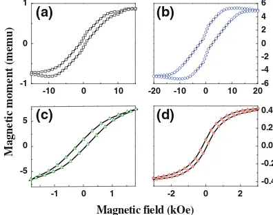
Electric field and excimer laser treatment have been observed to have strong effects on the magnetization reversal behavior of 50-nm nickel thin films. Coercive field has changed drastically by such nanostructuring tech-niques. Coercive field value and technical saturation magnetic moment value for untreated 50-nm nickel thin film were found to be 1.17 k Oe and 0.87 memu (Fig.4a). Technical saturation magnetic moment is where virtually it is almost saturating, i.e. where the hysteresis loop ends meaning thereby the divergence ends, and single line of magnetization starts as one progresses in magnetic field. Actual saturation is reached at very large magnetic field though. These values (coercive field and technical
Fig. 2 AFM image in DFM
mode showing the nanostructures formed by various nanostructuring techniques forauntreated 50-nm nickel thin film,belectric field treatment,cexcimer laser treatment anddtrench-template assisted technique
Fig. 3 Grain size distribution calculated from AFM images for
[image:4.595.197.547.57.373.2] [image:4.595.58.547.64.514.2]saturation magnetic moment) for laser nanostructured nickel thin film are 0.15 kOe and 2.1 memu (Fig.4c), respectively. For the electric field nanostructured nickel thin film, the corresponding values of coercive field and technical saturation magnetic moment are 2.5 kOe and 4.85 memu (Fig.4b).
Trench template grown nanowires sample show the coercive field value and technical saturation magnetic moment value of 0.25 kOe and 0.44 memu, respectively. The net area over which the nickel material is available on the substrate is substantially very small for the templated growth case when compared to the untemplated thin film growth case. Moreover, area of hysteresis loop (magneti-zation energy density) and saturation magnetic moment/ coercive field ratio can also be derived. It has been observed that the hysteresis areas for the cases namely, as-deposited and untreated thin film case, electric field nanostructured thin film case, excimer laser nanostructured thin film case and trench-template assisted technique, are 1.8, 10, 0.3 and 0.2 (kOe memu) units, respectively. These areas reveal the magnetization energy density. It can be seen apparently that electric field of the value used for the treatment in this experiment can give rise to magnetization energy density approximately 5 times higher than that of the untreated thin film. Saturation magnetic moment/coercive field ratio are 0.74, 1.94, 6.66 and 1.76 memu/kOe units. This ratio has to do with the shape and hence squareness of the magnetic hysteresis loops.
Discussion
Even though energy density for the laser irradiation case is extremely higher than the DC electric field case, exposure
time for excimer laser is very low (in the order of nano-second) when compared to that for the electric field case (time of the order of few seconds). This gives rise to rapid quenching kind of effect for the excimer laser irradiation case. Since the area exposed by the film for excimer laser beam is very large, virtually whole film is getting exposed, because no focusing was done for this purpose. Laser nanostructuring thus can give rise to reproducible large area modification of thin film surface. Crystal growth is frozen midway, as soon as laser exposure is off. For electric field case however, field was treated for 20 s continuously. Joule’s heat accumulates in the thin film and in the direction of current path (where resistance is mini-mum), and thus the heat experienced by nanoparticles on the surface is more when compared to the case of laser irradiation. As a result of electric field treatment, material undergoes diffusion from one site to another and ultimately material assembles in the line of electric field. In the present case, the value of electric field (in the order of kV/ cm) is not sufficient for electro migration to occur where huge electric field (2 orders of magnitude higher than the present case) is required. However, due to high electric field gradient setup between the line of current and radially away from it, thermo migration occurs and is the possible origin of surface reconstruction. Metal nanoparticles behave as dielectric and gets polarized and that is the origin of organization of nanoparticle as has been discussed in details elsewhere [36]. Magnetization has been observed to be larger (5 times), and coercive field has also been observed to be larger (approximately double) for electric field nanostructured nickel thin films when compared to that for the untreated nickel thin film. This kind of obser-vation can be explained based on the magnetically aniso-tropic nature of the organized nanodots.
Thin film area remaining on BSG substrate after lift-off of resist (maleic acid) is approximately 1/50th of the ori-ginal as-deposited nickel thin film. Therefore, trench-tem-plate grown nanowires show very less magnetic moment as shown in Fig.3d. However, if the moment be multiplied 50 times for the sake of comparison, it results in magnetic moment approximately twice of that for the as-deposited continuous nickel thin film. Surprisingly, coercive field value for the nanowire sample is just 1/5th of that for the continuous nickel thin film. This demonstrates the better magnetic switching capability of nanowires.
Excimer laser apart from giving rise to grain growth has been known to alter magnetic response of the material momentarily. However, this complex phenomenon of excimer–laser material interaction and its impact on mag-netic behavior has still scope for lot of studies to be done. Recently, Muller et al. [38] have investigated the influence of the nanoscale on laser-induced magnetization dynamics in nickel. It has been experimentally observed in the
-1 0 1
-6 -4 -2 0 2 4 6
-5 0 5
-10 0 10 -20 -10 0 10 20
-1 0 1 -2 0 2
-0.4 -0.2 0.0 0.2 0.4
(a)
(c) (d)
(b)
Magnetic moment (memu)
Magnetic field (kOe)
Fig. 4 Magnetic hysteresis loop for 50-nm thermally evaporated
[image:5.595.69.267.61.217.2]present research that the magnetic moment increases approximately 2.5 times when compared to that for the untreated nickel thin film. Also, coercive field for laser nanostructured Ni thin film is smaller than that for the untreated thin film. Grain size primarily determines the domain size and therefore, inter-domain interaction is going to be governed by the grain size and separation. Coercive field being the measure of the ease for magneti-zation reversal depends on both the criteria grain size and grain separation. In laser nanostructured case, grain sizes are visibly large but grain wall width has thinned down heavily. This makes domain interaction easier and hence smaller coercive field.
In our case, it was not actually single nanowire case, inside the 5-micron-diameter trench template, approxi-mately 11–12 nanowires were formed as was observed in SEM and reported elsewhere [38]; which makes nanowires magnetically interacting with each other. Ordered sets of interacting ferromagnetic nanowires are complex systems which require numerical simulations for the investigation into their micromagnetic properties. Applying finite ele-ment techniques, combined with the boundary eleele-ment method, allows to accurately calculate the magnetostatic interaction between several magnetic nanowires. It turns out that for an array of wires, the coercive field is signifi-cantly lower than that for a single nanowire. Time-resolved micromagnetic simulations are employed to study the dynamics of the magnetization reversal of single nano-wires. With increasing diameter, a nucleation–propagation process is replaced by a curling reversal mode [39,40].
Volume of material, anisotropic growth features, flat-ness of the grains resulted, size, shape and separation of grains and finally different extent of oxidation; these are the factors basically responsible for different magnetic behaviors shown by the nickel thin films nanostructured by different techniques. For example, for trench template technique, it is expected that due to shadowing effects, limited material would get access inside the trench tem-plate when compared to that for the regular random growth features outside the trench. The extents of oxidation for usual thin film growth outside the trench and inside the trench are expected to be same, since not much different conditions of oxygen availability is speculated. Anisotropic growth features in trench template grown nanowires how-ever are held primarily responsible for different kinds of magnetic behavior. Electric field-induced and excimer laser-induced techniques however are expected to effec-tively evaporate (etch out) the material, and hence material volume reduction is speculated. Among these two tech-niques, excimer laser technique has yielded almost isotro-pic kind of grain growth features, while on the other hand electric field-induced technique has yielded anisotropic grain growth features. Isotropic flat grains in excimer laser
case have not been saturated at small field. In electric field case however, grains are relatively higher (large height/ diameter ratio) and not in contact with each other and apart from all this grains are organized in electric field direction too. This makes electric field nanostructured thin film magnetically different from the excimer laser nanostruc-tured nickel thin film.
Excimer laser and electric field both are high energy density triggers. Apart from the nanostructure growth and modifications, it gives rise to annealing effects usually due to heat generated. Excimer laser for example gives rise to extreme heating (approximately 3,000°C for short period of time (nanoseconds)) and electric field on the other hand gives rise to comparatively slow heating (1,000°C in few seconds). However, in the specified electric field range for the experiments carried out here, rate of heating will not be as a matter of fact that much slow though. Annealing in such conditions gives rise to crystalline growth. Annealing usually gives rise to lower coercive fields and higher rel-ative magnetization [41] (normalized magnetization). Due to the laser etching and electric field etching effects for nickel thin films in particular, thicknesses of the grains too change and it becomes flatter than before. This effect adds to a so many factors already available for the system under consideration including that of the oxidation. Thus, such extreme energy density triggers can give rise to surface nanostructure growth and modification, surface oxidation (few atomic layers), enhanced overall crystallinity, etching of the grains and relaxation of strains [42]. These are some reasons [43] to count with for the changes observed in magnetic behavior for nickel thin films.
Conclusions
In conclusion, nanostructuring techniques (employing DC electric field, excimer laser and trench template technique in controlled manner) give rise to different morphological modifications (directional nanostructuring for electric field treatment, isotropic growth features for excimer laser treatment and nanowire growth for trench-template assisted technique) for thermally evaporated 50-nm nickel thin film. Such morphological modification has strong impact on magnetization and magnetization reversal behavior.
Acknowledgements Authors would like to acknowledge University
of Hyderabad for the facilities used for the purpose. Financial support from University grants Commission (UGC) and Department of Sci-ence and Technology (DST), Government of India is duly acknowledged.
Open Access This article is distributed under the terms of the
References
1. H. Gleiter, Acta Mater.48, 1 (2000)
2. M.E. McHenry, D.E. Laughlin, Acta Mater.48, 223 (2000) 3. H. Gleiter, Prog. Mater. Sci.33, 223 (1989)
4. S.J. Henley, C.H.P. Poa, A.A.D.T. Adikaari, C.E. Giusca, J.D. Carey, S.R.P. Silva, Appl. Phys. Lett.84, 4035 (2004)
5. J.G. Cheng, J. Wang, T. Dechakupt, S.T. McKinstry, Appl. Phys. Lett.87, 232905 (2005)
6. O.V. Overschelde, R. Snyders, M. Wautelet, Appl. Surf. Sci.254, 971 (2007)
7. T.R. Jervis, J.P. Hirvonen, M. Nastasi, J. Mater. Res.6, 1350 (1991)
8. P.P. Donohue, M.A. Todd, Z. Huang, Integr. Ferroelectr.51, 39 (2003)
9. S.S.M. Chan, M.D. Whitfield, R.B. Jackman, G. Arthur, F. Goodall, R.A. Lawes, Semicond. Sci. Technol.18, S47 (2003) 10. K. Brendel, N.H. Nickel, P. Lengsfeld, A. Schopke, I. Sieber, M.
Nerding, H.P. Strunb, W. Fuhs, Thin Solid Films427, 86 (2003) 11. E. Hontzopoulos, E. Damigos, Appl. Phys. A: Mater. Sci.
Pro-cess.52, 421 (1991)
12. W. Xianyu, H.S.Y. Cho, J.Y. Kwon, H. Yin, T. Noguchi, IEICE Trans. Electron.E89-C(10), 1460 (2006)
13. A.A.D.T. Adikaari, S.R.P. Silva, M.J. Kearney, J.M. Shannon, Mater. Res. Soc. Symp. Proc.836, L8.2.1 (2005)
14. Z. Jiang, H. Wang, H. Huang, C. Cao, Chemosphere 56, 503 (2004)
15. L. Gaudart, R. Rivoira, Appl. Opt.12, 1897 (1973)
16. K.S. Novoselov, A.K. Geim, S.V. Morozov, D. Jiang, Y. Zhang, S.V. Dubonos, I.V. Grigorieva, A.A. Firsov, Science 306, 666 (2004)
17. T. Xu, A.V. Zvelindovsky, G.J.A. Sevink, K.S. Lyakhova, H. Jinnai, T.P. Russell, Macromolecules38, 10788 (2005) 18. M. Weisheit, S. Fa¨hler, A. Marty, Y. Souche, C. Poinsignon, D.
Givord, Science315, 349 (2007)
19. S. Loreti, D. della Sala, M. Garozzo, Micron31, 299 (2000) 20. D.H. Cobden, Nature409, 32 (2001)
21. Y. Cui, C.M. Lieber, Science291, 851 (2001)
22. G.A. Prinz, Science282, 1660 (1998)
23. G. Schmid, L.F. Chi, Adv. Mater.10, 515 (1998)
24. M.V. Kamalakar, A.K. Raychaudhuri, J. Nanosci. Nanotechnol. 9, 5248 (2009)
25. S.H. Xue, Z.D. Wang, Mater. Sci. Eng.: B135, 74 (2006) 26. S. Xue, C. Cao, H. Zhu, J. Mater. Sci.41, 5598 (2006) 27. I.M.L. Billas, A. Chaˆtelain, W.A.D. Heer, Science 265, 1682
(1994)
28. R.H. Kodama, J. Magn. Magn. Mater.200, 359 (1999) 29. D.L.L. Pelecky, R.D. Rieke, Chem. Mater.8, 1770 (1996) 30. D. Farrell, Y. Cheng, S. Kan, M. Sachan, Y. Ding, S.A. Majetich,
L. Yang, J. Phys.: Conf. Ser.17, 185 (2005)
31. H. Zeng, C.T. Black, R.L. Sandstrom, P.M. Rice, C.B. Murray, S. Sun, Phys. Rev. B73, 020402R (2006)
32. R.M. Metzger, M. Sun, G. Zangari, M. Shamsuzzoha, Mat. Res. Soc. Symp. Proc.636, D9.33.1 (2001)
33. T.T. Shafir, G. Markovich, J. Chem. Phys.123, 204715 (2005) 34. M.G. Krishna, P. Kumar, Non-lithographic techniques for
nano-strcturing thin films and surfaces. in Emerging nanotechnology for manufacturing, ed. by W. Ahmed, M.J. Jackson (Elsevier Sciences, Amsterdam, 2009). ISBN no. 9780815515838 35. P. Kumar, M.G. Krishna, A. Bhattacharya, Int. J. Nanosci.7, 255
(2008)
36. P. Kumar, Employing electrical energy in nanotechnology. in Encyclopedia of nanoscience and nanotechnology, ed. by Prof. H.S. Nalwa (American Scientific Publishers, California, 2009) 37. P. Kumar, M.G. Krishna, A.K. Bhatnagar, A.K. Bhattacharya, Int.
J. Nanomanuf.2, 477 (2008)
38. G.M. Mu¨ller, G. Eilers, Z. Wang, M. Scherff, R. Ji, K. Nielsch, C.A. Ross, M. Mu¨nzenberg, New J. Phys.10, 123004 (2008) 39. R. Hertel, J. Kirschner, Phys. B: Condens. Matter343, 206 (2004) 40. H. Riccardo, J. Mag. Mag. Mater.249, 419 (2002)
41. C.A. Neugebauer, Phys. Rev.116, 1441 (1959)
42. G. Dixit, J.P. Singh, R.C. Srivastava, H.M. Agrawal, R.J. Cho-udhary, A. Gupta, Surf. Interface Anal.42, 151 (2010) 43. P. Kumar, M.G. Krishna, A.K. Bhattacharya, Bull. Mater. Sci.32,