A High-Gain and Low-Noise 0.9 µW
Operational Amplifier
Milad Piry
1,*, Mona Khajani Moaf
2, Parviz Amiri
21Department of Electrical Engineering, Sharif University of Technology, Tehran, Iran 2Department of Electrical Engineering, Shahid Rajaee Teacher Training University, Tehran, Iran
*Corresponding Author: milad-piry@ee.sharif.edu
Copyright © 2014 Horizon Research Publishing All rights reserved.
Abstract
A low-voltage, low-power, high-gain and low-noise operational transconductance amplifier (OTA) by modifying conventional one is presented and analyzed. Design strategies are discussed for minimizing noise and increasing gain. The simulation results show that the open loop gain is improved from 68 dB to 74 dB and the input referred noise is also reduced from 926 nV / Hz to 475/
nV Hz . This amplifier operates at 0.8 V power supply voltage with a power consumption of 0.9 µW. All the simulations are obtained by using Hspice tool with 0.18 µm CMOS TSMC parameters.
Keywords
Transdonductance Amplifier, High Gain Op-Amp, Low Noise, Low Voltage, Low Power1. Introduction
In recent years, much effort has been put into the reduction of supply voltage and the supply power of mixed signal CMOS systems [1]. Three main reasons can be given for the advent of low-voltage circuits [2]. As a first reason, since the channel length is scaled down into submicron and gate-oxide thickness is decreased dramatically, in order to ensure the device reliability, the supply voltage has to be reduced. As a second reason, because of increasing number of components implanted on a single chip, the power per electronic function is increased. Since a silicon chip can
only dissipate a limited power per unit area, the power consumption has to be lowered. The third reason is dictated by portable and battery-powered equipment. The supply power and the supply voltage have to be reduced to have an acceptable operation period from a battery.
The low noise operational amplifier is one of the most essential parts of analog circuits. In MOSFET devices, there are two important noise sources, which are flicker noise (below 1MHz) and thermal noise [3], [4]. Designing a high dc gain and low noise CMOS OTA with a low supply voltage is very complicated. In this paper by using a simple modification the gain and noise of conventional OTA are improved with the constant power consumption.
The proposed OTA is described in section 2. In section 3 a design procedure is presented. In section 4 proposed circuit has been simulated using the models of the TSMC 0.18 µm technology and a comparison of proposed OTA with conventional one and other configurations is summarized. The paper is concluded in section 5.
2. Proposed OTA
A
[image:2.595.169.443.72.471.2]B
Figure 1. (A) Proposed OTA. (B) Conventional OTA.
[image:2.595.128.482.481.740.2]Fig. 2 shows the current variations versus input differential voltage vi2-vi1. It can be observed that the circuit
works as a differential amplifier in part of the input signal. Voltage gain of the proposed OTA is given by:
10 2 4 2 4 10 9
A
Vd=
g
m(
g
m+
g
m)( || )(
r
or
or
o|| )
r
o (1) It is almost two times larger than the open-loop gain of conventional OTA with the same power consumption which is equal to:10 2 2 4 10 9
A
Vd=
g g
m m( || )(
r
or
or
o|| )
r
o (2) The noise contribution of the second stage of the opamp is negligible, because it is divided by the gain of the previous stage when referred to the input [5]. Also noise contribution of current source is negligible. Thus thermal noise per unit bandwidth [6] produced by transistors is almost given by:2 1 4
1 3
1
|
2 4
n M
m m
V
kT
g
g
γ
−
= ×
×
+
(3)2 7 8
7 8 2 2 2
1 3 7 1 3
|
4
(
m)
m( || )
n Mm m m o o
g
g
V
kT
g
g
g
r
r
γ
−+
=
×
+
(4)2 9 10
9 10 2 2 2
1 3 10 1 3
|
4
(
m)
m( || )
n Mm m m o o
g
g
V
kT
g
g
g
r
r
γ
−+
=
×
+
(5)Thus input-referred thermal noise Power Spectral Density (PSD) of the proposed OTA and conventional OTA can be written as:
2 9 10
2 2
1 3 1 3 10 1 3
8
(1
)
(
)
(
m)
m( || )
thermal
m m m m m o o
g
g
kT
V
g
g
g
g
g
r r
γ
+
=
+
+
+
Proposed OTA (6)
2 3 9 10
2 2 2 2
1 1 1 10 1 3
1
8
(
)
( || )
m m m
thermal
m m m m o o
g
g
g
V
kT
g
g
g g
r r
γ
+
=
+
+
Conventional OTA (7) Where k is the Boltzmann’s constant, T is the temperature in kelvin. The coefficient γ is equal to 2/3 for long channel transistors and it needs to be replaced by a larger value for submicron MOSFETs. It also varies to some extent with the drain- source voltage [3].
Input-referred flicker noise PSD of the proposed OTA and conventional OTA can be shown as (8) and (9) respectively, where COX is capacitance per unit area of the gate oxide,
KfN is NMOS flicker noise coefficient and KfP is PMOS
flicker noise coefficient. It can be observed that total input-referred noise in proposed OTA is much smaller than conventional one.
In this work all transistors are biased in weak inversion to have large gm in addition of low power consumption. Since
opamps are usually designed to be operated with negative-feedback connection, frequency compensation is necessary for closed-loop stability. The frequency compensation of proposed OTA is easily achieved like the conventional one [7].
The main drawback of this OTA is its limited input signal caused by transistors M3 and M4, which is equal to:
2 4
sat
SS DS GS i DD SG
V
+
V
+
V
≤
V
≤
V
−
V
(10) Input signal swing is one threshold voltage smaller than conventional OTA, that is because of transistors M3 and M4. Note that if the output signal is taken from nodes A or B, for ideal current source M5, CMRR is given by:2 2
9 10
2 9 10 2 2
ker 2 2 2 3 1
1 3 10 2 4 3 1
(
)
(
)
2
(
)
( || )
(
)
(
)
+
=
+
+
+
fN fP m m fP fNflic m m
OX m m m o o
K
K
g
g
K
K
WL
WL
V
g
g
C f g
g
g
r
r
WL
WL
Proposed OTA (8)2 2
9 10 2
2 9 10 3
ker 2 2 2 2
1 10 2 4 3 1 1
(
)
(
)
2
( || )
(
)
(
)
+
=
+
+
fN fP m mfP m fN
flic
OX m m o o m
K
K
g
g
K
K
WL
WL
g
V
C f
g g
r
r
WL g
WL
Conventional OTA (9)2 4 2
4 4 2
(
)
2
mm(
o m oo)
g
g
r
CMRR
g
r
r
+
=
+
(11)For ro2= ro4 it is approximated by:
2 4 4
4
m m mg
g
CMRR
g
+
=
(12)3. Design Procedure
For gm9=gm10 and gm1=gm2=gm3=gm4 noise spectral density
can be written as:
2
1 10 1 3
8
( )
3
( || )2
n
m m o o
KT
S f
g g
r
r
=
(13)Gain-Bandwidth product is almost equal to:
1 10 1 3
4
m m( || )
o oL
g g
r
r
GB
C
=
(14)DC gain is also given by:
2 0
4
m1 m10( ||
o1 o3)
A
=
g g
r
r
(15) From (13) and (14) we obtain0 1
||
3o o L
A
r
r
GB C
=
×
(16)Substitute gm10from (14) and the above equation into (13)
yields:
1
0
32
3 ( )
mn
KT
g
S f A
=
(17)2
10
3(
128
L)
n( )
mGB C
S f
g
KT
×
=
(18)Since transistors are operating in subthreshold region, we have: D m T
I
g
NV
=
(19)0
( / )
DC
I
I
I W L
=
(20)Where N is subthreshold coefficient, VT, thermal voltage, IC,
inversion coefficient (which shows the operation region of transistor, for IC>1 in strong inversion, for 0.1< IC<1 in
moderate inversion, for IC<1 in weak inversion), I0,
normalized current in subthreshold region (which is equal to
2
2
N C V
µ
ox T ).From (17), (18), (19) and (20) we obtain:
1 4 1
0
( )
Tm C
NV
W
g
L
−=
I I
(21)7,10 10
0
( )
TC
NV
W
g
L
=
I I
(22)4. Simulation Results
The proposed OTA was simulated with the supply voltage of VDD = 0.35 V and VSS = - 0.45 V. For the simulations, 0.18
µm CMOS technology parameters were used. The biasing current source was 1 µA. All the devices used have 0.5 µm length (three times the lowest value for the employed topology). The inversion coefficient of transistors is IC1,2 =
0.103 and IC3,4 = 0.256, thus these transistors are in moderate
[image:4.595.60.552.101.418.2]inversion. Table 1 summarizes widths of the transistors used in the proposed circuit. Table 2 summarizes specifications of the circuit resulted from simulations and compares them with the conventional OTA and other configurations.
Table 1. Width for the transistors used in the proposed OTA
MOS W(µm)
M1,M2 15
M3,M4 28
M5 1
M7,M10 2
M8,M9 0.3
Bode plot of the OTA is shown in Fig. 3. It can be observed that, since the DC gain is increased and bandwidth is constant, the unity gain-bandwidth product is larger than conventional OTA, however, phase margin is decreased.
Fig. 4 shows the transient characteristic of the proposed structure with a capacitor load of 10 pF when a square signal of 0.6 VPP at 2 MHz is applied at the input of unity-gain
configuration of OTA. The slew rate is 0.8 V/µs which is equal to slew rate of conventional OTA.
Fig. 5 shows the equivalent input referred noise, it can be observed that the input referred noise is significantly lower than conventional OTA. Fig. 6 shows the total output noise voltage which is obvious that the proposed OTA has better performance than conventional one. Fig. 7 shows the measured response for a 100 Hz, 20 µV peak-to-peak sinusoidal input voltage. The measured THD was -44 dB.
Table 2. Simulation results summary
Proposed OTA Conventional OTA [8] [9] [10] [11]
Voltage Supply 0.8V 0.8V 0.8V 0.5V 0.8V 0.8V Technology
(CMOS) 0.18 µm 0.18 µm 0.18 µm 0.18 µm 0.18 µm 0.35 µm DC Gain 74dB 68dB 51dB 55dB 68dB 66dB
UGBW 1MHz
CL=10pF 0.61MHz CL=10pF CL=10pF 40 kHz 8.72 MHz CL=10pF 8.12 MHz CL=1 pF 3.4 MHz CL=5 pF Phase Margin 42o 56o 65o 89o 89o 80o
Slew Rate CL=10pF
f=2MHz 0.8 V/µs 0.9 V/µs 0.12 V/µs 1.35 V/µs 2.89 V/µs 4.7 V/µs FOM=
(CL*Slew Rate) /Power pF.V/µs.µW 8.3 pF.V/µs.µW 10
2.34
pF.V/µs.µW pF.V/µs.µW 0.18 pF.V/µs.µW 0.03 pF.V/µs.µW 0.12
Power Consumption 0.9µW 0.9µW 1 µW 77 µW 94 µW 194 µW Gain/Power Consumption 82.2 dB/µW 75.5 dB/µW 50.8 dB/µW 0.71 dB/µW 0.72 dB/µW 0.34 dB/µW
Input referred noise
@215Hz
nV
475/
Hz
nV
926/
Hz
- - - -BW 285Hz 285Hz - - - -
CMRR 33dB 50dB - - - -
B
Figure 3. Frequency response of proposed OTA (continuous line) and conventional OTA (dotted line) (A) Phase. (B) Gain.
[image:6.595.93.518.415.707.2]Figure 5. Equivalent input noise at Vi2.
[image:7.595.91.520.80.691.2]Figure 7. Output of the proposed OTA with 20µVPP sinusoidal input voltage.
B
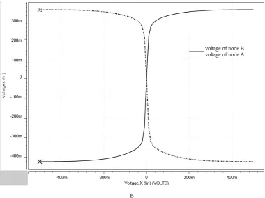
Figure 8. Voltage of nodes A and B vs. differential input voltage Vi2-Vi1: (A) Proposed OTA. (B) Conventional OTA
5. Conclusion
A low-voltage and low-power OTA was proposed in this paper, which was modified version of conventional OTA. By using a simple modification, the voltage gain and noise performance were significantly improved, however the CMRR and input signal swing range in comparison to conventional OTA decreased. The simulation results showed that the DC gain is two times larger than conventional OTA and input referred noise is two times lower than conventional one.
To demonstrate the feasibility and scalability of the design a standard 0.18 µm CMOS process with very restrictive supply voltage of 0.8V has been used.
REFERENCES
[1] S.S. Rajput, S.S. Jamuar, Low Voltage Analog Circuit Design Techniques, Circuits and Systems Magazine, IEEE , Vol. 2, No. 1, 24-42, 2002.
[2] C.J.B. Fayomi , M. Sawan, G.W. Roberts, A Design Strategy for a 1-V Rail-to-Rail Input / Output CMOS OpamV, Proc. International Symposium on Circuits and Systems (ISCAS), Vol. 1, 460 – 463, 2001.
[3] B. Razavi, Design of Analog CMOS Integrated Circuits. New York, NY: MCGraw-Hill,2001.
[4] S. Martin, V.D. Archer III, D.M. Boulin, M.R. Frei, K.K. Ng, R.H. Yan , Device Noise in Silicon RF Technologies,
Bell Labs Technical Journal, Summer 1997.
[5] A. Soltani, M. Yaghmaie, B. Razeghi, R. Pourandoost, S.I. Tous, A. Golmakani, Three Stage Low Noise Operational Amplifier Design for a 0.18 um CMOS Process, 9th International Conference on Electrical Engineering, Computing Science and Automatic Control (CCE), 1-4, 2012.
[6] G. Giusi, F. Crupi, C. Pace, P. Magnone, Full Model and Characterization of Noise in Operational Amplifier, IEEE Transactions on Circuits and Systems I:Regular Papers, 97-102, Vol. 56, 2009.
[7] Zuschu Yan, Pui-In Mak, R.P. Martins, Two Stage Operational Amplifiers: Power and Area Efficient Frequency Compensation for Driving a Wide Range of Capacitive Load, Circuits and Systems Magazine, IEEE, Vol. 11, Issue. 1, 26-42, 2011.
[8] M. R. Valero, S. Celma, N. Medrano, B. Calvo, C. Azcona , An Ultra Low-Power Low-Voltage Class AB CMOS Fully Differential OpAmp, IEEE International Symposium on circuits and systems (ISCAS), 2012.
[9] S. Chatterje, Y. Tsividis, P. Kinget, A 0.5-V bulk-input fully differential operational transconductance amplifier, Proceedings of the 30th European Solid-State Circuits Conference (ESSCIRC), 2004.
[10] J. Rosenfel, M. Kozak and E. G. Friedman, A bulk-driven CMOS OTA with 68 dB DC gain amplifier, Proceedings of the 11th IEEE International Conference on Electronics, Circuits and Systems, 2004.
[image:9.595.115.496.75.359.2]