CALIFORNIA INSTITUTE OF TECHNOLOGY
Pasadena, California
2011
© 2011
This dissertation not only reflects the countless hours spinning photoresist, cleaning parylene machines, and mixing epoxy in Caltech Micromachining Laboratory, but it is also a conglomeration of years of wonderful experiences, opportunities, lessons, and valuable encounters during my PhD career. This endeavor would not be possible if it were not for my families, my friends, my mentors, my colleagues, and all those whom I have met over the past years.
Coming to Caltech was one of the best decisions I have made. The lab was not just a research lab to publish papers, it was also a place to nurture students to be ethical, logical engineers; it was a shelter to develop a fearless mind and become a hands-on researcher; and most important of all, it was a sanctuary to foster good thinkers who can solve any problem that they encounter. I have learned so much beyond what was written in books and papers, and I would not have been able to do so if I were not in this lab.
Dr. Tai, you have taught me so much; not just about how to be a good scientist, but you have guided me on acquiring a positive and forward-thinking attitude that has encouraged me and supported me through the toughest time. I want to express my sincerest gratitude and appreciation to you; thank you for the advice, the leadership, the support, and having faith in me. It was my honor to have you as my advisor.
My thanks also go to Christine Garske, Agnes Tong and Tanya Owen, thank you for your help in purchasing and administrative tasks. You have made the life of all members in the lab so much easier and smoother. Thanks to Mr. Trevor Roper, without whom we would not have any device we have made to date.
I also want to give credit and my appreciation to Dr. James Weiland and Dr. Ellis Meng, and USC students including Artin Petrossians, Alice Cho, Lauren Hickey, Christian Gutierrez, Dr. Brian Li and Dr. Ronalee Lo, who have dedicated their time and effort in advancing the research program in both USC and Caltech and have helped me tremendously in my research endeavor in BMES ERC.
brother who have always been there for me and have given me unconditional support over the years in every aspect of my life. Words cannot simply describe my sincerest gratitude and appreciation to them. Thank you.
packaging technologies are developed and presented to enable a new generation of flexible neural implants. These technologies can also house integrated circuit chips and provide high-density electrical connection to it.
This packaging scheme utilizes the parylene-metal-parylene skin structure and can be totally integrated and be monolithically fabricated with existing functional devices. The size and the electrode patterns can be modified to suit different chips and applications. Integration with flexible cable integrated silicon probes for neural prosthesis, implantable muscle stimulators and implantable RFID tagging technology are all successfully demonstrated in this dissertation. Other discrete components can also be integrated to achieve high level functionality.
1 INTRODUCTION ... 1
1.1 PROSTHETIC APPLICATIONS—THE NEED AND DRIVING FORCE ... 1
1.1.1 Retinal Prosthesis ... 1
1.1.2 Neural Prosthesis ... 2
1.2 INTEGRATION TECHNOLOGY... 3
1.2.1 Traditional Chip Integration Technology ... 4
1.2.2 State-of-the-Art Chip Integration Technologies with Biodevices ... 6
1.3 PROBLEMS AND CHALLENGES ... 12
1.4 MEMS TECHNOLOGY ... 14
1.4.1 Bulk Micromachining ... 17
1.4.2 Surface Micromachining ... 19
1.4.3 Introduction to Parylene ... 20
1.4.4 Parylene for MEMS and Biomedical Applications ... 24
1.5 PROSTHETIC INTERFACE TECHNOLOGY THRUST ... 26
1.6 LAYOUT OF THE DISSERTATION ... 27
1.7 SUMMARY ... 28
2 PARYLENE POCKET TECHNOLOGY ... 29
2.1 INTRODUCTION ... 29
2.2 POCKET DESIGN—PARYLENE VS. SILICON SUBSTRATE ... 30
2.3 FABRICATION ... 32
2.3.1 First Generation... 32
2.3.2 Second Generation—Silicon Substrate ... 35
2.3.3 Second Generation—Parylene Substrate ... 36
2.3.4.1 For IC Chips ... 38
2.3.4.2 For Discrete Components ... 40
2.3.4.3 For Double Side and Multiple Layer Components ... 41
2.4 INTEGRATION WITH SILICON PROBES ... 45
2.4.1 Design ... 47
2.4.2 Fabrication ... 50
2.4.3 Testing and Verification ... 52
2.5 SUMMARY ... 55
3 IMPLANTABLE CHIP INTEGRATION TECHNOLOGY ... 56
3.1 INTRODUCTION ... 56
3.2 RFID CHIP INTEGRATION ... 57
3.2.1 Design and Fabrication ... 58
3.2.2 Integration Demonstration... 60
3.2.3 Functional System Testing ... 62
3.3 BION CHIP INTEGRATION ... 64
3.3.1 Design and Fabrication ... 65
3.3.2 System Integration Demonstration ... 66
3.3.3 Functional System Testing ... 68
3.4 CONCLUSION ... 70
4 PACKAGING, ACCELERATED LIFETIME TESTING AND MODELING . 71 4.1 INTRODUCTION ... 71
4.2 PARYLENE TO SILICON INTERFACIAL ADHESION ENHANCEMENT ... 72
4.2.1 Sample Preparation ... 74
4.2.2 Experiments... 75
4.2.2.1 Partial Film Peeling Test ... 76
4.2.2.2 ASTM Standard Tape Peeling Test ... 78
4.2.2.3 Accelerated Soaking Tests ... 80
4.2.2.4 HF Soaking Tests... 82
4.2.2.5 Conclusion ... 82
4.3 ACCELERATED LIFETIME SOAKING TEST OF PROTECTED ICS ... 83
4.3.1 Samples Preparation ... 84
4.3.2 Passive Soaking ... 85
5.2 PARYLENE POCKET ON SILICON SUBSTRATE ... 107
5.2.1 Fabrication ... 107
5.2.2 Fabrication Challenges ... 109
5.2.2.1 Lift-off Metal Patterning ... 109
5.2.2.2 Thick Photoresist for Plasma Etching ... 113
5.2.2.3 Parylene Cracking... 114
5.2.2.4 Metal Line over a Step... 116
5.2.2.5 Pocket Size ... 117
5.3 PARYLENE POCKET ON PARYLENE SUBSTRATE ... 118
5.3.1 High Density Integration ... 120
5.3.1.1 Alignment ... 120
5.3.1.2 Squeegee Technique ... 121
5.3.2 Integration Issues ... 126
5.3.2.1 Metal Pad on Edge ... 126
5.3.3 Repairs and Enhancements ... 128
5.3.3.1 Laser Fix (Short Circuit)... 128
5.3.3.2 Conductive Epoxy Failures ... 131
5.4 FUNCTIONAL TESTING ... 132
5.5 CONCLUSION ... 135
6 CONCLUSION ... 137
LIST OF FIGURES
Figure 1.1. Soldering a component onto the back of a printed circuit board. ... 4
Figure 1.2. Gold wire bonded onto metal pads to make electrical connections. ... 5
Figure 1.3. Illustration of the ball grid array; the BGA on an actual IC chip. ... 6
Figure 1.4. The Michigan three-dimensional neural probe array [40]; SEM picture of the tip of the Michigan probe [33]. ... 7
Figure 1.5. Concept of embedded chip integration; overall view of the device; close-up view of the embedded chip; close-up view of the coil wires. ... 8
Figure 1.6. Close-up picture of the MicroFlex bonding technique, facilitated by a commercial wire bonding machine setup [70]. ... 10
Figure 1.7. Final implant with parylene C and silicone rubber encapsulation [71]. ... 10
Figure 1.8. Schematic representation of the retinal implant by Theogarajan et al. [73]. .. 11
Figure 1.9. (a) Schematic of the three-dimensional stacked chip [74]; (b) implantable sensor system: A control unit and analogue part with RF coil [75]. ... 12
Figure 1.10. Comparison of positive and negative photoresist. ... 16
Figure 1.11. Comparison of surface micromachining and bulk micromachining. ... 17
Figure 1.12. Comparison of isotropic and anisotropic wet etching and dry etching. ... 18
Figure 1.13. Examples of silicon bulk micromachining; the substrate material is etched away to create different features [81]. ... 19
Figure 1.14. An example of surface micromachined gears [82]. ... 20
Figure 1.15. Chemical structures of parylene N, C, D, and HT, and some of the correlated process parameters used in parylene deposition system PDS 2010 and 2060. ... 21
Figure 1.16. Parylene deposition system and its deposition process. ... 22
Figure 1.17. Permeability vs. time of different materials. ... 25
Figure 1.18. Proposed all-intraocular system for high density epiretinal implant. ... 27
of the parylene pocket from the silicon substrate. ... 34 Figure 2.6. Insertion of the IC chip into the parylene pocket; tweezers are used to align
the bonding pads to the metal pads on the chip under the microscope. ... 35 Figure 2.7. Alignment of the pads on the parylene pocket and the metal lines on the
inserted chip. The alignment offset was on the order of 10 to 20 μm; a drop of biocompatible conductive epoxy is applied over the metal pads to provide electrical conduction. The size of the drop is on the order of 150 to 200 μm. ... 36 Figure 2.8. Bonding scheme for the parylene pocket. A drop of conductive epoxy is
applied on the bonding hole that exposes the metal pads on the IC chip underneath. 36 Figure 2.9. Fabrication process for the pocket structure with parylene C substrate. The
device can be made on any type of wafer. ... 37 Figure 2.10. Parylene pocket-only structure. This device is used to test the amplifier chip after bonding. Signal is driven in from the bonding pads on the right-hand side of the figure and is measured from the bonding pads on the left-hand side of the figure. ... 39 Figure 2.11. Parylene pocket-only structure. It is used to test the amplifier chip after
bonding. Signal is driven in from the bonding pads of the parylene structure on the right-hand side of the figure. ... 39 Figure 2.12. Input of 5 mV (10 mV peak to peak) sine wave of 1 kHz is passed into the amplifier (gain = 60) and its oscilloscope output is recorded. Signals of 0.5, 2, and 5 kHz were also tested with the chip. ... 39 Figure 2.13. Circuit diagram of the RLC circuit packaged with the parylene pocket. ... 40 Figure 2.14. Parylene pocket on parylene substrate for discrete components. An RLC
Figure 2.15. Measured frequency response of the RLC circuit, the resonance frequency can be clearly determined from the plot; measured phase response of the RLC circuit. ... 41 Figure 2.16. Fabrication process for dual layer pocket. ... 43 Figure 2.17. (a) Fabricated dual layer parylene pocket device for PCB integration; (b)
PCB inserted into the pocket. The insertion process is similar to the process described in previous sections. ... 43 Figure 2.18. Close-up view of the PCB inserted into the pocket. One can clearly see the traces on the right-hand side run underneath the PCB whereas the traces on the left hand side run above the PCB; a side-to-side comparison of the front and back of the device. ... 44 Figure 2.19. Current metal bonding pad orientation; the metal pads on the bottom layer
point away from the bottom surface. ... 44 Figure 2.20. Ideal metal bonding pad orientation; the metal pads on the bottom layer
point toward the bottom surface. ... 45 Figure 2.21. Schematic of cortical implantation using neural probes with parylene cables.
... 46 Figure 2.22. SEM picture of the electrodes on the silicon shanks; probe stacking
capability of the silicon probe structure. Figure shows three 32-channel probes stacked together to form a 96-channel three-dimensional structure. The spacing between the probes can be modified. ... 47 Figure 2.23. Single microelectrode pin with parylene coating. The only electrode is
opened at the tip of the probe. ... 48 Figure 2.24. Released silicon probe with parylene flexible cable. ... 48 Figure 2.25. Proximal bonding of commercial connector with parylene cable connector
pads; before bonding; after bonding with conduction epoxy. ... 49 Figure 2.26. Bonding interface of the connector pads on the silicon probe device and the commercial connector through a custom PC board. ... 49 Figure 2.27. Schematic of the packaged silicon probes. The design shows a 96-channel device consisting of three 32-channel devices. The legs of the titanium pedestal are secured to the skull with bone screws. ... 49 Figure 2.28. Fabrication process of the parylene-cabled silicon probe with parylene
Figure 2.32. Successful chronic implantation in rat cortex by penetrating pia using a complete device with metal electrodes and flexible parylene cables. The picture
shows the silicon probe being inserted halfway into the brain. ... 53
Figure 2.33. (a) Silicon probe-only structure for testing purpose. The parylene sheet extension provides metal pads for electrical connection to the parylene pocket-only structure; (b) bonded and packaged structure. In this device, the conduction chip was used. The impedance of the electrode was measured to be 600 kΩ. ... 54
Figure 3.1. CMOS MEMS integrated process [119]. ... 57
Figure 3.2. EM4100 RFID chip used to demonstrate the pocket integration technology. 58 Figure 3.3. Photolithography masks used for the RFID parylene pocket structure; lift-off lithography mask for the metal; metal exposure mask; through hole and device definition mask; sacrificial layer mask. Positive photoresist is used is this process. . 60
Figure 3.4. Step-by-step integration process of the RFID chip with the parylene pocket. 61 Figure 3.5. Parylene pocket packaged RFID chip. The structure is coated with 30 μm parylene C and around 1.5–2.0 mm of biocompatible silicone after bonding. ... 62
Figure 3.6. RFID test setup with the oscilloscope. ... 63
Figure 3.7. Signal readout from the oscilloscope. ... 63
Figure 3.8. BION chip layout and the pad connection. ... 65
Figure 3.9. Schematic overview of a BION chip integration system. ... 65
Figure 3.10. Mask layout for the parylene pocket structure for the BION chip. ... 66
Figure 3.11. Chip pad arrangement; two-dimensional arrangements; one-dimensional arrangement. ... 66
Figure 3.13. Packaged BION chip in the parylene substrate. ... 68 Figure 3.14. A telemetry setup for functionality test of the assembled BION system; the complete set up with the personal trainer and the transmitting coil; the receiving coil sitting inside the transmitting coil. ... 69 Figure 3.15. Typical simulation pulse measured from the electrode site. ... 69 Figure 4.1. Delamination occurs on an integrated parylene-cabled silicon probe and may eventually separate the parylene and the silicon probe; delamination on the edge of an integration chip with parylene layers on top. The performance of the pocket is compromised due to the separation of parylene and silicon. The white arrows point out the difference in color, which indicates saline undercut. ... 73 Figure 4.2. Process steps for different treatment; all of the process steps start with a
500 μm thickness prime silicon wafer that goes through the treatment and then has parylene deposited on top of it. The control sample of this experiment has parylene deposited on top of a blank wafer without any type of treatment. ... 75 Figure 4.3. Sample layout for soaking tests. The diameter of the circle is 6.8 mm; sample layout for peeling tests (3 mm × 5.7 mm). For those used for peeling tests, photoresist is used as sacrificial layer to create the partial film. All trenches are 250 μm wide; actual samples. ... 75 Figure 4.4. Partial film torn before the film is peeled away from the substrate; partial film completely peeled away. ... 77 Figure 4.5. Time vs. force plot of a parylene film being pulled away from the silicon
substrate. Section A is the elastic part of the pulling process, where section B represents rupture and C represents the residual constant force. ... 77 Figure 4.6. Molten adhesion layer sample (after testing) for pulling test; SEM of the
peeled interface. ... 78 Figure 4.7. ASTM cross-cut test; XeF2 treated surface with parylene before 120ºC one
hour soaking; after Scotch tape peeling, parylene on the treated surface is still intact. The circular shape surfaces in the samples are XeF2 treated surfaces. ... 80
Figure 4.8. Annealed sample with molten adhesion layer 90ºC soaking result. ... 81 Figure 4.9. Sample with molten adhesion layer 90ºC soaking result; the trench is 200 μm wide. Nonannealed samples have lower undercut rate than their annealed counterparts ... 81 Figure 4.10. XeF2 treated samples after 48% HF cleaning for 1 minute; 10 minutes. The
residue can be seen coated on the side of the container; this effect is not observed in
sample coated with parylene and biocompatible silicone. ... 93
Figure 4.18. Active soaking of parylene pocket that houses an RFID chip. ... 94
Figure 4.19. Fabrication step of parylene-only structures for mechanical model. ... 95
Figure 4.20. Custom heat-forming mold. ... 96
Figure 4.21. First generation completely intraocular model. ... 97
Figure 4.22. First generation completely intraocular model in porcine eye. ... 97
Figure 4.23. Design of the part intraocular, part extraocular model. The gold wire sits outside the eyeball while the rest of the systems are implanted inside. ... 98
Figure 4.24. Prototype geometry for a part intraocular, part extraocular parylene-based device with all required component regions for a completely implantable system. .. 99
Figure 4.25. The power coil made from gold wires; the intraocular lens acting as data coil in this mechanical model. ... 99
Figure 4.26. Example of a coil with intraocular coil haptics attached. ... 99
Figure 4.27. Chip packaging in parylene pocket in mechanical implantation model; parylene sheet before assembly with chip inserted; thickness of the chip section is approximately 1.6 mm; parylene pocket after biocompatible silicone coating; the parylene pocket after curing and annealing. ... 100
Figure 4.29. Retinal tack used for attaching the parylene electrode sheet onto the retina surface; view from outside of the eyeball. One can clearly see the tacks coming out; retinal tack. ... 101 Figure 4.30. Intraoperative surgical photographs; the parylene electrode area being
inserted into the opening; the parylene pocket with chip being inserted into the opening; the intraocular lens being inserted; the opening being sutured, leaving the gold wire power coil outside. ... 102 Figure 4.31. Postsurgery dissection of the eyeball. ... 102 Figure 5.1. (a) Layout of 256-channel stimulation chip from UC Santa Cruz. The pad size is 100 μm × 100 μm. There are about 120 functional peripheral pads on the edge of the chip; (b) dummy chip with conductive traces is fabricated to emulate the actual chip. ... 106 Figure 5.2. Printed circuit board integration approach with parylene pocket platform for
retinal prosthetic prototype testing. ... 107 Figure 5.3. Process step for the parylene pocket platform on silicon substrate. ... 108 Figure 5.4. Layout of the parylene pocket on silicon substrate platform. ... 109 Figure 5.5. Fabricated parylene pocket platform with silicon substrate with chip
Figure 5.19. The squeegee is used to push the excess conductive epoxy away from the surface; heat is applied to cure the epoxy that remains in the trench to make the connection between the pads of the parylene and the IC chip. ... 123 Figure 5.20. The conductive epoxy may short circuit two neighboring metal pads on the
chip if the viscosity of the epoxy is too low; the conductive epoxy may not provide electrical connection if the viscosity is too high. ... 123 Figure 5.21. The well after the conductive epoxy squeegee process. The well is only
5 microns tall and cannot retain the epoxy, leaving empty spaces in the well. After SU-8 layer application, the wells are completely retained and filled. ... 123 Figure 5.22. The conductive epoxy footprint on a testing substrate after squeegee process. This test is conducted to determine the optimized aspect ratio of the SU-8 well. ... 124 Figure 5.23. The surface profile of the bonded surface. The maximum height of the
conductive epoxy bump is about 25 µm ... 125 Figure 5.24. The surface of the bonding pads right after the squeegee. There is a
significant amount of residue left. ... 125 Figure 5.25. Edge of the chip—where the squeegee process may become a problem. .. 127 Figure 5.26. Chip edge protection process: PDMS is poured on top of the IC chip and
Figure 5.31. Short circuit defect repair process; laser is used to first open the parylene, followed by a short etch of the metal excess in between the metal lines. ... 130 Figure 5.32. (a) Shortage of neighboring metal pads underneath the parylene film due to low viscosity of the conductive epoxy; (b) even though the surface of the parylene film is free of conductive materials. ... 131 Figure 5.33. After ultraviolet laser cleaning. The laser cuts through the film and clears
Table 4.3. Result of the ASTM cross-cut test (n = 2). ... 79
Table 4.4. Accelerated life time testing to observe the undercut rate of the parylene/silicon interface (n = 3). ... 81
Table 4.5. MTTF of conduction chips in different packaging. ... 87
Table 4.6. MTTF of conduction chips in parylene pocket (estimation assumes an Arrhenius activation energy factor of 2 for every 10ºC). ... 92
Table 4.7. MTTF of conductive epoxy adhesion on different surfaces. ... 94
Table 5.1. Step height effect on metal continuity. ... 117
Table 5.2. Aspect ratio of conductive epoxy well and its connectivity. ... 124
GLOSSARY
ACIOL – anterior chamber intraocular lens AMD – age-related macular degeneration
ASCII – American Standard Code for Information Interchange ASIC – Application Specific Integrated Circuit
ASTM – American Society for Testing and Materials BGA – ball grid array
CL-I2 – Chip-level Integrated Interconnect
CMOS – complementary metal–oxide–semiconductor CT – computed tomography
CVD – chemical vapor deposition DIP – dual in-line package
DRIE – deep reactive ion etching EDP – ethylene diamine pyrocatechol FDA – Food and Drug Administration HF – hydrofluoric acid
HNA – hydrofluoric acid, nitric acid and acetic acid IC – integrated circuit
ID – identification
ISO – International Organization for Standardization KOH – potassium hydroxide
LIGA – Lithographie, Galvanoformung, Abformung (Lithography, Electroplating, and Molding)
PSG – phosphosilicate glass RF – radio frequency
RFID – radio frequency identification RIE – reactive ion etching
RLC – resistor-inductor-capacitor RP – retinitis pigmentosa
SEM – scanning electron microscope SNR – signal-to-noise ratio
SOI – silicon on insulator
TMAH – tetramethylammonium hydroxide TTL – transistor-transistor logic
1
INTRODUCTION
1.1
Prosthetic Applications—The Need and Driving Force
1.1.1 Retinal Prosthesis
Two of the most common retinal degenerative defects in the world right now are age-related macular degeneration (AMD) and retinitis pigmentosa (RP). RP has already affected several hundreds of thousand people in the United States to date and AMD is estimated to cause more than several million people worldwide to have significant symptoms associated with it in the next ten years [1–3]. Even though gene therapies, drug and nutritional therapies and other types of remedies are developed [4–5] to decrease the rate of such occurrences, the defects still cause the loss of the rod and cone receptors in the eye [4, 6–8], and blindness in the long run becomes inevitable and cannot be treated.
It has been studied, however, that the ganglion cell layer, which consists of the optical nerves, remains functional even after the patient has gone completely blind and can be electrically stimulated to construct localized visual signals in patients [9–12]. Visual prosthesis, a technology that takes advantage of this fact to regains eyesight for AMD, RP and patients with other degenerative eye diseases, quickly becomes the focus for research and development around the world.
1.1.2 Neural Prosthesis
Diseases, traumatic incidents and natural defects cause the interruption of information flow between the brain, nerves, spinal cords, muscles and sensors in human body. This disconnection have been one of the top priorities for research with goals to develop treatments and rehabilitation methods to either reverse, treat or to alleviate the symptoms and to improve the quality of life of the patients. As early as the 18th century, it was discovered that the use of external electrical stimulation has the potential to overcome paralysis [15]. Since then, a series of technical aids such as neural prosthesis have been developed to bridge the gap between the generation of the biological signals from the brain and the stimulation of the muscles.
connects the different parts of the system. Silicon probe systems developed by University of Michigan [24–46], University of Utah [47–54] and SOI probe [55–58] and polymer probe systems [59–62] all have reported functionality and recording/stimulating capabilities in animal subjects and are expected to make great contributions in neural prosthesis research.
Finally, both neural and retinal prosthetic application are expected and required to be biostable and biocompatible. In-depth research is currently being conducted to realize a fully functional and reliable long-term implantation that is able to both record and stimulate neurons to achieve a total neural prosthetic system.
1.2
Integration Technology
assembling larger scale, general circuit components. Some specific technologies for bonding IC chips with devices that are used in biomedical fields and more specifically, prosthetic applications are also presented.
1.2.1 Traditional Chip Integration Technology
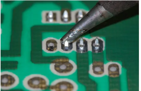
[image:27.595.198.437.433.588.2](a)Soldering
Figure 1.1. Soldering a component onto the back of a printed circuit board. (Courtesy of Wynn Rostek)
dirty bonding of discrete components, but the physical weakness of the solder bonding, toxicity of the materials, localized heat during assembly and its inability to connect small and dense array pads makes soldering a less attractive alternative than other more advanced technologies.
(b)Wire Bonding
Wire bonding is considered one of the most cost effective, flexible and efficient interconnect technology to be used in making connection between a printed circuit board and an integrated circuit chip after soldering technology. In wire bonding, a metal wire (usually gold, aluminum or copper) is fed through the wire bonding machine application tip and is pressed onto the target metal contact pads with electrically generated heat or ultrasonic vibration to form electrical and mechanical contact (figure 1.2). This step is repeated again at the second point of contact to complete a bond. This technology is most useful and most cost efficient in making small number of connection on big substrates and is most commonly used in bonding bare dies in DIP packages.
Figure 1.2. Gold wire bonded onto metal pads to make electrical connections.
(c) Ball Grid Array
with this technology.
Figure 1.3. (left) Illustration of the ball grid array; (right) the BGA on an actual IC chip. (Image courtesy of ThomasNet and Dominic Plunkett from www.xjtag.com)
1.2.2 State-of-the-Art Chip Integration Technologies with Biodevices (a) University of Michigan—The Michigan Probes
K. D. Wise at University of Michigan has developed a variety of penetrating electrode in different layouts for neural prosthetics. This endeavor started as early as 1969 in Stanford University [32] and has evolved into complete systems fully integrated with IC circuitries on the same silicon substrate (figure 1.4). The interconnections of these circuitries are made with a ~4–5 μm thick polysilicon cable. Weaknesses of this silicon-film cable are apparent since they are too brittle and are prone to breakage.
Flip-Chip Solder Balls Underfill
The silicon probes developed at the University of Michigan have recently adapted polymer cables [65]. These silicon probes are fully capable of simulating and recording from neural tissues and muscles. Much in vivo testing on animal subjects has been successfully conducted. However, the devices are still very difficult to make and require expensive process and equipment to realize; mainly due to the low yield in combining CMOS and MEMS process and the cost of materials.
On the other hand, University of Michigan has recently developed technologies to create electrical connection to a chip that is made separately from the cable and the probe itself [66], signifying a need for improvement for a higher density and easier bonding technique.
Figure 1.4. (left) The Michigan three-dimensional neural probe array [40]; (right) SEM picture of the tip of the Michigan probe [33].
(b)California Institute of Technology—CL-I2
devices tested with histology results have also been published to verify the overall biocompatibility and the feasibility of the sandwich layer technology.
However, the alignment problem that arises during the “chip-drop” could severely affect the feasibility of this technology. Not only would the surface flatness inside the cavity limit the metal connectivity over a step, but the low alignment efficiency of the bonding pads on the chip with the metal in the parylene sandwich layer renders the integration inefficient.
Figure 1.5. Concept of embedded chip integration; (left) overall view of the device; (middle) close-up view of the embedded chip; (right) close-up view of the coil wires.
(c) Microflex Interconnect
Microflex (MFI) is an interconnect technology developed by the Fraunhofer Institute for Biomedical Engineering; Meyer et al. [68] utilizes a polyimide substrate with
Parylene C Foundry Fabricated Chip & Passive Components
Silicon Housing
photolithography patterned metal embedded in it. The pitch and the shape of the metal pads correspond to the bonding pads on the chip. The via-hole on the substrate contact pads is then filled with metal balls or wedges applied by a commercial wire bonder to make the electrical and mechanical contact. This technology, though very similar to wire bonding, is specifically developed to integrate the passive and active electronic components to the electrodes (figure 1.6).
Since this technology is based on polyimide process, it is compatible for biomedical implants. This substrate has passed cytotoxicity testing according to ISO 10993, has been soaked more than 4 years in saline solution and has been implanted for more than 10 months in rats. The MicroFlex technology can also be applied to three-dimensional structures and the density is comparable to that of the flip chip technology. Several ultrasound array sensors, retinal stimulators (EPIRET) and multiplexer modules have been integrated successfully with this technology [68–71].
Their current device, called the EPIRET 3, has transmitting coils on external glasses and an internal receiver coil and chip secured in the eye in place of the lens (figure 1.7). As with all epiretinal prosthesis, the electrode array is tacked onto the back of the retina. In an exploratory human trial in 2009, the device was implanted for four weeks to observe the safety of the device and how well it would work. There was mild inflammatory response in some of the six subjects, but they decided there was no lasting damage from the prosthesis. Four of the six subjects gained light perception, one gained hand movement, and one had no light perception [72].
Figure 1.6. Close-up picture of the MicroFlex bonding technique, facilitated by a commercial wire bonding machine setup [70].
Figure 1.7. Final implant with parylene C and silicone rubber encapsulation [71].
(d)Boston Retinal Implant Project
connections between the flex circuits and the electrode arrays. Nonconductive epoxy was used to encapsulate the entire device and then coated in PDMS (polydimethylsiloxane).
Although this device has been through several in vivo studies, the integration approach proved to be prone to reliability problems. Also, the lifetime of the encapsulation coating (PDMS) has subpar performance relative to other biocompatible coatings.
Figure 1.8. Schematic representation of the retinal implant by Theogarajan et al. [73].
(e) Other Technologies
Deguchi et al. from Tohuku University in Japan have developed a one-piece, stacked retinal prosthesis chip system to be implanted in human eye [74]. It consists of implantable IC chips responsible for photodetection, image processing, current generation and stimulating arrays (figure 1.9a). While implanting the entire chip into the eye eliminates the need for integration of flexible electrodes with circuitry, the hard substrate that comes along with this stacking technology makes it more damaging to the tissues and less surgically friendly.
A pressure monitoring system integrated in a small package has been developed by Schlierf et al. [75]. The package comprises a sensor ASIC, which includes a capacitive
Testing Pads
Discrete Capacitors for Power Supply
Schottky Diodes
Return Electrode
Flexible Substrate
Data and Power Coils
varieties of biomedical implants and prosthetic devices. The basic idea is to minimize the number of electronic components and the size of the packaging without compromising the functionality of the overall device. While many of these devices have good functionality and short-term stability, clinical trials still needs to be demonstrated for both animal and human models for long-term reliability and performance evaluations.
Figure 1.9. (a) Schematic of the three-dimensional stacked chip [74]; (b) implantable sensor system: A control unit and analogue part with RF coil [75].
1.3
Problems and Challenges
Next generation retinal prosthesis development will require totally implanted devices to minimize inflammations and surgical complexity as well as the physical damages incurred on the receiving subject during surgeries and procedures. This means the
(b) (a)
Vertical Interconnection
Adhesion Layer Stimulus Electrode MOSFET
telemetry circuit, along with signal processing and the stimulation circuit and a stimulation electrode all would have to eventually be fit inside a human eyeball (<1–2 cm3). MEMS
technology, which will be discussed in the next section, is not only a great candidate to miniaturize the system, but it has also been utilized to increase the precision and the ease of fabrication of such implantable devices. In fact, MEMS has become one of the most crucial technologies that would foster the success of the development of a reliable implantable system.
However, although numerous implantable devices have been developed with micro-electrical-mechanical system technology to integrate IC with bioimplantable microfabricated devices, there still lacks an enabling packaging technology that is able to meet all of the requirements that are demanded by current state-of-the-art retinal and neural implantable systems. First of all, the analog/digital driving electronics must be in a hermetic package/encapsulant, protected from the saline environment of the body since this package needs to address the long-term biocompatibility and reliability issue in the human body. It is necessary to develop a technique to protect these implanted components from the corrosive substances, like body fluid. As it is discussed later in the chapter, parylene C, a biocompatible polymer, is selected as the main structural and packaging material because of its many favorable properties. By doing so, the package will be mechanically stable within the tissue without causing damage either to the device or to the patient.
(ASICs), capacitors, etc.) and can withstand adverse human implant environment reliably for many years. The insulating material must not corrode, dissolve, or leak; parylene C, a MEMS compatible material, provides just the right solution to solve this problem.
In conclusion, it is clear that for the state-of-the-art implantable systems on this scale, it has become not only a trend, but a necessity to utilize MEMS technology to fabricate microelectrodes and its packaging schemes. The next section will be devoted to the discussion of this technology with a focus on parylene.
1.4
MEMS Technology
miniaturization. The design of MEMS is different from the design of systems of a larger scale. This is due to the fact that the surface area of a miniaturized structure is much greater than its volume and causes the reduction of mass and inertial volume effects but increases the electrostatic and wetting surface effects of the system.
There are countless advantages from using MEMS technology. Not only does it enable the communication between mechanical and electrical elements on the same substrate in a system, it also has lower cost, is smaller in size, mass and power consumption, and has higher functionality, reliability and precision. Because of these advantages, numerous devices such as micromotor [77], accelerometer [78], pressure sensors [79] and RF filters are realized.
Figure 1.10. Comparison of positive and negative photoresist. (Courtesy of NCSU Soft lithography Wiki)
Figure 1.11. Comparison of surface micromachining and bulk micromachining.
1.4.1 Bulk Micromachining
Bulk micromachining takes advantage of all three dimensions of the bulk material and creates features inside the substrate (top-down machining) by etching. Single crystalline silicon is the most common material used in MEMS processing because of its ability to be easily etched. Etching can be separated into two categories: isotropic etching and anisotropic etching; both of these etchings can be achieved in a wet or dry environment (figure 1.12).
(Courtesy of An Introduction to MEMs Engineering—Nadim Maluf and Kirt Williams) Etching can also be achieved by dry etching, which can be separated into three classes called reactive ion etching, sputter etching and vapor phase etching depending on the different chemical and physical interactions between the ions of the gas and the atoms on the substrate. In reactive ion etching, external energy generated by RF (radio frequency) power induces chemical reaction in low-pressure reaction chambers between the gaseous ions and the atoms on the target substrate. Some physical bombardment of the gaseous ion onto the target substrate also occurs. In this process, gases such as chlorofluorocarbon gases, sulfur hexafluoride, bromine compounds and oxygen are commonly used as reactants. Sputter etching, on the other hand, is very similar to reactive ion etching, except that the process is made up entirely of the physical bombardment of the ions without any chemical interactions. In vapor phase etching, the substrate is placed inside the chamber where the gas is present, and is dissolved at the surface in a chemical reaction with the gas molecules. This process is made possible by using XeF2 [80] (xenon
difluoride) or a mixture of interhalogen gases (such as BrF3), which provide very high
Figure 1.13. Examples of silicon bulk micromachining; the substrate material is etched away to create different features [81].
1.4.2 Surface Micromachining
Surface micromachining, unlike bulk micromachining where features are inside the substrate, is based on the deposition and etching of different structural layers on top of the substrate (bottom-up processing). Because the process does not depend on the etching characteristic of the substrate, different materials such as soda lime, silicon on insulator and metals are sometimes used in this process.
Figure 1.14. An example of surface micromachined gears [82].
Finally, by combining steps of material deposition, photolithography, material etching/removal, and necessary cleaning steps, two-dimensional masks can be used to extrude and fabricate complex devices in three dimensions.
1.4.3 Introduction to Parylene
Parylene is deposited at room temperature with a chemical vapor deposition process called Gorham process [84]. In this vacuum process (~25–35 mT, to increase mean free path to the substrate) (diagrammed in figure 1.16), raw dimer material is placed in a vaporizer furnace, and evaporated to a dimeric gas at approximately 130 to 150ºC. This gas then passes through a high-temperature pyrolysis (~650 to 750ºC) furnace, where the molecule is split into monomers. The monomers enter a chamber that is held at room temperature, and polymerize on all exposed surfaces in the chamber conformally without pinholes. Residual monomer is collected on a cold trap before it enters the mechanical vacuum pump to prevent damage. Parylene coating thickness often ranges from several hundreds of nanometers to tens of micrometers and can be controlled by the amount of the dimer placed in the evaporation chamber. By changing the deposition chamber pressure, the deposition rate and the density of parylene can also be controlled. Different variants of parylene require varying process conditions, but the method remains essentially the same.
Figure 1.16. Parylene deposition system and its deposition process.
The properties of the different species of parylene are listed in table 1.1 to compare with PDMS (polydimethylsiloxane), a material that has been traditionally used in biomedical applications. Not only is parylene superior in many aspects than PDMS and polyimide [85] such as pinhole-free conformal deposition, low gas and water vapor permeability, and chemical inertness, it is also transparent in the visible light range. These desirable characteristics make it a perfect candidate for protecting implanted devices and electronics from corrosive agents and body fluids. With Young’s modulus of 2–3 GPa and an elongation-to-break percentage of more than 200%, parylene C also acts as a perfect membrane material for large deflection applications.
Class VI material (the highest biocompatibility rating for plastics in the United States). Parylene HT is the new favorite with its excellent thermal stability, water barrier property, high ultraviolet stability, better electrical and crevice penetration property, lower coefficients of static and kinetic friction, and is also ISO 10993 biocompatible [87– 88].
Table 1.1. Properties of parylene N, C, D, HT, and PDMS. (Table and data adopted from [89–91])
Property Parylene N Parylene C Parylene D Parylene HT PDMS
Dielectric Strength
(V/mil), 1 mil film 7,000 5,600 5,500 5,400 610 (1 mm film) Dielectric Constant 60 Hz 1 kHz 1 MHz 2.65 2.65 2.65 3.15 3.10 2.95 2.84 2.82 2.80 2.21 2.20
2.17 2.3–2.8
Young’s Modulus (psi) 350,000 400,000 380,000 -- 52–126
Index of Refraction 1.661 1.639 1.669 -- 1.4
Yield Strength (psi) 6,100 8,000 9,000 -- 325
Elongation to Break (%) 20–250 200 10 -- 210–310
Coefficient of Friction Static Dynamic 0.25 0.25 0.29 0.29 0.33 0.31 0.145 0.130 -- 0.43–0.51 Density (g/cm3)
1.10–1.12 1.289 1.418 -- 9.7 × 10⁻⁴
Melting Point (ºC) 420 290 380 >450 −49.9–40
Thermal Conductivity at 25ºC
(10−4 cal/(cm × s × ºC))
3.0 2.0 -- -- 3.6
Water Absorption (% after 24 hours)
< 0.1 < 0.06 < 0.1 < 0.01 --
(depends on cure conditions)
Specific Heat at 20ºC (cal/g × ºC)
need electrical insulation and lubrication to reduce friction as well. Thus, the biocompatibility of the packaging material that is in contact with tissue is crucial and important to the overall stability of the system.
Numerous packaging materials have been investigated to serve this purpose in many implantable applications such as pacemakers, cochlear implants, etc. From the permeability study by Ko et al. and Kazemi et al. [92–93], metal has the best hermetic sealing of electronics to be implanted in human body while generic silicone and epoxies have relatively inferior performances (figure 1.17). However, the listed materials may not meet toxicity and/or biocompatibility requirements and cannot be applied with precise control.
and implantable devices. In addition, parylene produces no cure forces (compared to silicone and epoxy), contains no additives (no catalyst, solvents, plasticizers), is inert (no metal oxidation), lubricious and is applicable to most materials that are stable in vacuum. Finally, parylene C is the longest (~3 years) proven protective biocompatible material [97].
Figure 1.17. Permeability vs. time of different materials.
[image:48.595.138.427.229.453.2]The possible uses of the main parylene variants for biological applications are summarized in table 1.2. It can be clearly seen that parylene C has become the choice of material to be used in biomedical and implantable device applications mainly for its biocompatibility and its good ability to block water. This further strengthens our case to use parylene C in the development of implantable device platform.
Table 1.2. Parylene coating functions for selected medical applications. (adapted from [86])
Property Parylene N Parylene C Parylene HT
Catheter mandrels Lubricity -- High temperature
stability Endoscopic devices Dielectric, lubricity -- --
Permeability (gm/cm-s-torr)
Thickness (cm)
Silicones
Silicones
Metals Glasses
Needles/syringes Lubricity -- Lubricity, water barrier
Cannulae Lubricity -- --
Analytical lab components
-- Chemical resistance,
biostability
-- Ocular implants -- Biocompatibility, water
barrier, dielectric, mechanical strength Biocompatibility, water barrier, dielectric, UV stability, process temperature stability
1.5
Prosthetic Interface Technology Thrust
The overall goal of this dissertation is to develop the necessary subsystems fabrication and packaging technologies to support the implementation of neural interfaces for recording and stimulating in the retinal and cortical implantable test beds. In order to enable the long-term communication between the outside world and the neural tissue, three technologies are developed: electrode technology, packaging technology, and radio-frequency (RF) communication technology. In particular, these interface technologies need to be uniquely designed for both the retinal prosthesis and the cortical implantable test beds.
pulses and a high density MEMS electrode array for the actual stimulation of the retinal neural cells. While the electrode array has already been invented by Dr. Damien Rodger and the RF coil fabrication technology has been invented by Dr. Wen Li in the Caltech Micromachining laboratory, this work will focus on the flexible MEMS parylene-based implantable technology for pocket chip integration and its functionality demonstration, which aims to contribute to the overall initiative of realizing all prosthetic system applications including the intraocular epiretinal implantation system.
Figure 1.18. Proposed all-intraocular system for high density epiretinal implant.
1.6
Layout of the Dissertation
Chapter 2 describes the pocket fabrication technology and then discusses the variety and the versatility of the flexible pocket structure. A full integration demonstration with a flexible parylene-cabled silicon probe for a brain-machine interface is also presented. Chapter 3 demonstrates total system integration with a commercially available muscle stimulator chip and a radio frequency identification chip and discusses, in depth, their integration and packaging process. The result of their functionality testing is also presented. Chapter 4 then presents the long-term packaging reliability and the mechanical characteristic of the pocket structure and the result of the expected lifetime experiment.
Epiretinal Multielectrode Array
High Lead-count Flexible Cable
Packaged ASIC
2
P
ARYLENE
P
OCKET
T
ECHNOLOGY
2.1
Introduction
by photolithography resolution, which offers the potential to achieve high-lead-count (>1,000) integration. As a result, we are able to fabricate IC packaged devices that are highly customizable, fully biocompatible, and easy to mass fabricate. This will facilitate future research in developing more complex bioimplantable systems.
2.2
Pocket Design—Parylene vs. Silicon Substrate
Figure 2.1. Basic structure for parylene pockets.
Figure 2.1 shows the basic structure of the parylene pocket. The basic principle behind parylene pocket fabrication is the same for both silicon and parylene substrate. In both processes, a parylene-metal-parylene sandwich skin [101] is deposited on the substrate with a sacrificial layer that resides in between. The sacrificial layer is removed by the end of the process to create the pocket cavity that accommodates external IC chips.
Pockets with parylene substrate and silicon substrate can be made depending on
application and physical size of the IC chip. From experience, chips that are very thin
Metal Traces
Pocket Area
Parylene-metal-parylene Sandwich Layer
(less than 250 μm) and have relatively small surface area (less than 2 mm × 2 mm) are easier to assemble and integrate with pockets with silicon substrate as it provides a good
mechanical support to maneuver the chips inside the pocket for alignment and bonding.
Pockets with parylene substrate are recommended for chips that are thicker and larger in
size, since the real estate required for silicon substrate grows exponentially as the
thickness and the size of the IC chip increases. For example, a pocket with parylene
substrate of 1 cm × 1 cm is able to accommodate a 5 mm × 5 mm × 700 μm IC chip when a pocket with silicon substrate would need a 2.3 cm × 1.6 cm real estate to achieve the same goal. It should be noted that only pocket structure with parylene substrate is
completely flexible, and is generally preferred in implantable applications.
The pocket presented first in this chapter was designed to fit a 500 µm thick, 0.5 mm × 0.5 mm sized 16-channel amplifier integrated circuit chip (figure 2.2) designed by Dr. Wentai Liu’s group in University of California, Santa Cruz [102]. The signals from 16 channels are amplified by the low-noise amplifier of voltage gain 50. The fabrication process of the parylene pocket for both silicon and parylene substrate are demonstrated. An assembly process was also developed to integrate and assemble these components into a fully functional platform for neural signal recording. The combined thickness of the parylene C skin [103] and pocket is 25 μm with gold metal connection traces embedded.
Numerous skin technologies have also been developed by other research groups
worldwide [104–106]. But we have found parylene to be the ideal candidate for our application because of its better mechanical properties and its superior soaking mean time
2.3
Fabrication
2.3.1 First Generation
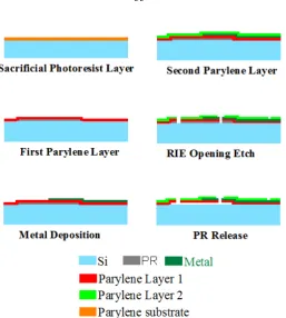
The parylene pocket configuration is fabricated with DRIE and RIE technology.
Figure 2.3 shows the fabrication process for parylene pocket with silicon substrate. First, a sacrificial photoresist layer is spin-coated on the silicon substrate for pocket releasing.
A bottom layer of parylene C (5 μm) is then deposited, followed by Cr/Au (0.05/0.2 μm) lift-off process with electron beam evaporation to provide electrical connection. The top
layer of parylene C (5 μm) is deposited to complete the parylene-metal-parylene sandwich skin structure. Electrode sites and the device definition are then opened by a
two-step RIE with O2 plasma process. The outline of the parylene pocket structure is
subsequently etched by DRIE with Bosch Process (Unaxis Corporation, St. Petersburg, FL, USA) [108] from both sides of the wafer. In the final step, the devices are released in photoresist stripper and dried. An IC chip is then inserted by hand into the parylene
Figure 2.3. Process steps for parylene pocket with silicon substrate. The entire pocket structure can be released from the wafer by DRIE or wafer dicing.
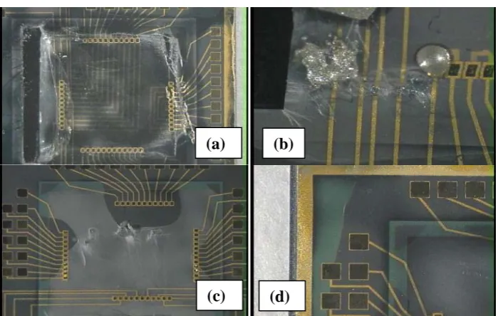
The first-generation parylene pocket, however, has some design flaws that prevent
it from functioning properly (the device is shown in figure 2.4). First of all, the pocket does not have enough stress relief to accommodate the thickness of the IC chip that is to
be integrated inside the pocket. The insertion process causes damage on the side of the
parylene pocket causing it to tear and break and would increase the chance of leakage and
compromises the packaging. The conduction traces on the side are also broken as a
consequence. In addition, the pocket area is not properly released due to the lack of
openings for the solutions to dissolve the photoresist underneath. This causes the pocket
to be physically stuck on the silicon substrate surface and prevents the chip from being
Figure 2.4. The first-generation parylene pocket with one opening on the side; all bonding pads are located on the chip.
Figure 2.5. Issues during fabrication and chip insertion; (a) chip insertion tearing the side of the pocket, causing breakage of the parylene; (b) open circuits in trace lines; (c) the parylene substrate is stuck on the surface of the silicon substrate; (d) delamination of the
parylene pocket from the silicon substrate.
Additional treatments such as melted parylene and parylene surface roughing are needed to ensure good adhesion between the sandwich skin layer and the substrate. After the devices are released and the IC chip integrated into the pocket, protective layers and biocompatible materials are deposited on the structure. Only after these protective
(a) (b)
treatments can we fully utilize these packaged IC chips in long-term implantation for prosthetic applications.
2.3.2 Second Generation—Silicon Substrate
In the second generation, stress relief openings are placed on both sides of the
pocket to facilitate the insertion of the chip (figure 2.6). After the chip is inserted by hand into the pocket, it is aligned (figure 2.7), bonded with conductive epoxy (figure 2.8) and totally coated with parylene C again for complete encapsulation and to ensure
biocompatibility. The fabrication step is similar to that of the version one pocket structure
with the exception of an additional melted parylene adhesion layer before the photoresist
coating to enhance bonding strength of parylene on silicon. This enhancement process
and its performance characterization will be discussed in length in chapter 4.
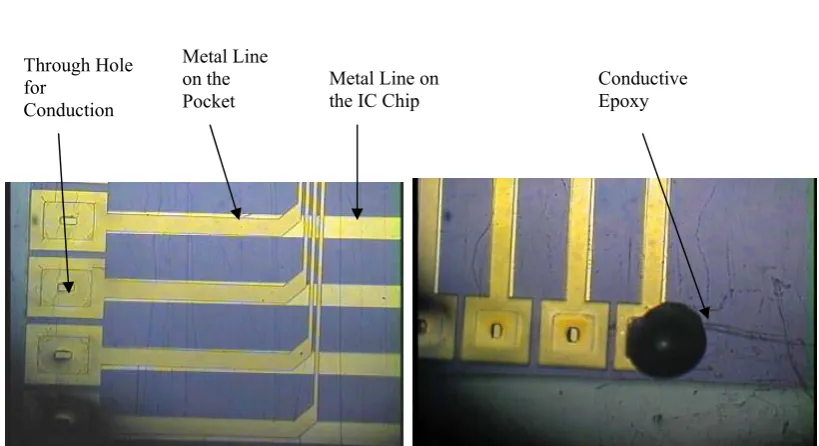
Figure 2.7. (left) Alignment of the pads on the parylene pocket and the metal lines on the inserted chip. The alignment offset was on the order of 10 to 20 μm; (right) a drop of
biocompatible conductive epoxy is applied over the metal pads to provide electrical
[image:59.595.110.520.84.307.2]conduction. The size of the drop is on the order of 150 to 200 μm.
Figure 2.8. Bonding scheme for the parylene pocket. A drop of conductive epoxy is applied on the bonding hole that exposes the metal pads on the IC chip underneath.
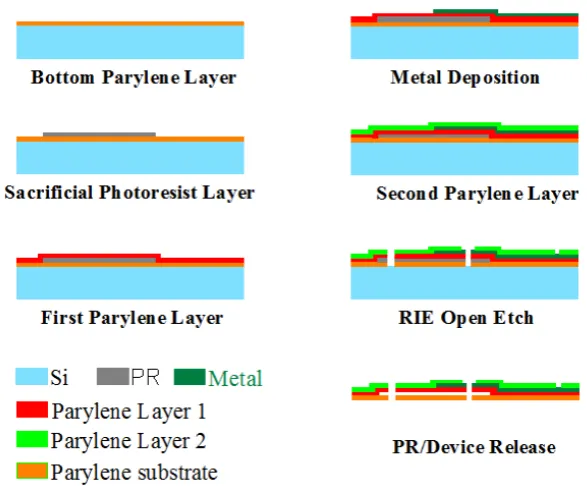
2.3.3 Second Generation—Parylene Substrate
The parylene pocket configuration is fabricated with RIE technology. Figure 2.9
shows the fabrication process for parylene pocket with substrate. First, 5 μm of bottom layer parylene C is deposited by room temperature CVD on a prime, untreated silicon
wafer. Sacrificial photoresist of 1 μm is then coated to create the parylene pocket structure. Another layer of parylene C (5 μm) is deposited, followed by Cr/Au (0.05/0.2 μm) lift-off process by electron beam evaporation to provide electrical
connection. The top layer of parylene C (5 μm) is deposited to complete the structure. Electrode sites and the device definition are then opened by a two-step RIE with O2
[image:60.595.166.460.187.430.2]plasma process. The devices are released in photoresist stripper.
Figure 2.9. Fabrication process for the pocket structure with parylene C substrate. The device can be made on any type of wafer.
It should be noted that the chip insertion and bonding process for parylene pocket on parylene substrate requires more steps than the bonding process for parylene pocket on silicon substrate due to the mechanical nature of the two structures. The parylene substrate lacks the mechanical backbone that the silicon substrate provides to support and fix the IC chip in place after insertion and leaves the IC chip too much freedom to move around in the pocket. An extra fixation process is thus developed to fix the parylene pocket on parylene substrate in place to facilitate the insertion and the alignment of the chip.
2.3.4 Variety of Pockets
On some occasions such as wireless telemetry and nerve stimulation, circuit components including capacitors and inductors are needed for the functionality of the overall system [109]. One of the biggest advantages of the parylene pocket over traditional packaging techniques is its ability to accommodate not only integrated circuit chips, but also different types of components such as printed circuit boards and surface mount components.
2.3.4.1 For IC Chips
The embedded CMOS amplifier chip [102] is a scalable 16-channel preamplifier
and buffer chip with an in-band gain of 35.5 dB. This chip was tested using a function generator on a pocket-only structure. Pockets with both silicon (figure 2.10) and parylene (figure 2.11) substrate are demonstrated here.
Both sine waves and square waves with frequency of 0.5, 1, 2 and 5 kHz and
amplitude of 5 mV were passed into the chip by connecting the function generator to the
bonding pads on the device. The amplified output (figure 2.12) from the oscilloscope concludes a successful functionality testing of our packaging technology for integrated
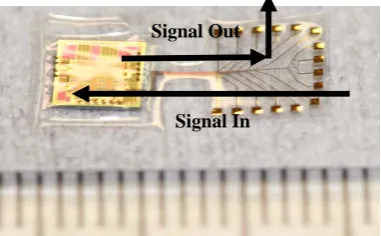
Figure 2.10. Parylene pocket-only structure. This device is used to test the amplifier chip after bonding. Signal is driven in from the bonding pads on the right-hand side of the
figure and is measured from the bonding pads on the left-hand side of the figure.
Figure 2.11. Parylene pocket-only structure. It is used to test the amplifier chip after bonding. Signal is driven in from the bonding pads of the parylene structure on the
right-hand side of the figure.
Figure 2.12. Input of 5 mV (10 mV peak to peak) sine wave of 1 kHz is passed into the amplifier (gain = 60) and its oscilloscope output is recorded. Signals of 0.5, 2, and 5 kHz
were also tested with the chip. Signal In
[image:62.595.198.433.465.671.2]Figure 2.13. Circuit diagram of the RLC circuit packaged with the parylene pocket. An RLC series circuit (figure 2.13) consisting of three 0.4 mm × 0.2 mm × 0.5 mm surface mount components (0402 package, Digikey Corporation, Thief River Falls, MN, USA) is packaged in parylene pockets with parylene substrate. The insertion and bonding process of the discrete components is exactly the same as that of the IC chips where conductive epoxy is used to make the connection from the bonding pads of the pocket and the contact pads of the surface mount components. The platform in figure 2.14 shows a 1 cm × 1 cm × 20 μm parylene substrate with three open pockets for the three surface mount components. The wafer bonding tape was used to assist the packaging and bonding of the structure.
The result for the impedance measurement of the circuit is shown in figure 2.15 with the following parameters: resistance = 1 kΩ, capacitance = 1 μF, inductance = 2.2 μH. The resonance frequency is calculated by the following equation,
√
This verifies the successful bonding of the circuit with the pocket and the overall functionality of the parylene pocket technology for discrete components.
Figure 2.14. (left) Parylene pocket on parylene substrate for discrete components. An RLC circuit with 0402 sized surface mount components is shown in the figure; (right) backside of the parylene pocket on parylene substrate. The surface mount components are
clearly shown inserted in the pocket.
Figure 2.15. (left) Measured frequency response of the RLC circuit, the resonance frequency can be clearly determined from the plot; (right) measured phase response of
the RLC circuit.
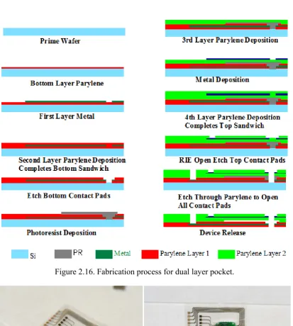
2.3.4.3 For Double Side and Multiple Layer Components
coated to create the parylene pocket structure. Another layer (3rd layer) of parylene C
(5 μm) is deposited, followed by another Cr/Au (0.05/0.2 μm) lift-off process with electron beam evaporation. The top (4th) layer of parylene C (5 μm) is then deposited to complete the top sandwich structure. Electrode sites and the device definition are then
opened by a two-step RIE with O2 plasma process. The devices are released in
photoresist stripper and warm water bath.
The fabricated device has dimension 2.6 cm × 2.6 cm with pocket size of 8.5 mm × 9.6 mm (figure 2.17a). The device thickness is around 25 μm with trace width of 200 μm and pad size 900 μm × 900 μm. These dimensions can be modified depending on the device. The insertion process of the PCB into the dual layer pocket is similar to the process described in previous sections. The integrated structure is shown in figure 2.17b.
Figure 2.16. Fabrication process for dual layer pocket.
Figure 2.17. (a) Fabricated dual layer parylene pocket device for PCB integration; (b) PCB inserted into the pocket. The insertion process is similar to the process described in
previous sections.
It should be noted that the metal on the bottom layer sandwich opens away from the surface (figure 2.19) and makes it more difficult to make connection. The conductive
Figure 2.18. (left) Close-up view of the PCB inserted into the pocket. One can clearly see the traces on the right-hand side run underneath the PCB whereas the traces on the left hand side run above the PCB; (right) a side-to-side comparison of the front and back of
the device.
Figure 2.19. Current metal bonding pad orientation; the metal pads on the bottom layer point away from the bottom surface.
Conductive epoxy Metal pads on the pocket
pointing away from the surface
Metal pads on the pocket pointing towards the surface
SURFACE
Figure 2.20. Ideal metal bonding pad orientation; the metal pads on the bottom layer point toward the bottom surface.
A quick conduction test of this structure verifies the functionality and the packaging ability of this technology. This dual layer structure not only can accommodate a double-sided PCB, it can also be extended to triple, quadruple or even more layers to incorporate ultrahigh density traces or multiple chip stacking applications. It would be possible to separate the control signal from the stimulation signal in a retinal prosthetic application, for example, to gain better control of the design of the system and to modularize the connections.
2.4
Integration with Silicon Probes
This section demonstrates a parylene pocket integrated silicon probe that is monolithically fabricated using MEMS technology. A schematic of the proposed implantation scheme is shown in figure 2.21.
Metal pads on the pocket pointing towards the surface Conductive epoxy
An important goal in neural prosthesis is to be able to decode the movement intention in the parietal cortex from neurons by implanting neuroprobes [110–111]. While three-dimensional integrated silicon probes have been successfully manufactured [112], the degradation of the signal-to-noise ratio (SNR) is still a major challenge because electronics are too far away from the recording site. Additionally, recent developments in bioimplantable devices such as retinal, cochlear and cortical prosthesis implants also increase the demand for totally implanted technologies. Therefore, the biocompatible parylene pocket technology becomes the perfect candidate for this application, as it is a suitable packaging/integration solution to embed amplifiers near the recording sites. A process to integrate parylene pocket onto a parylene-cabled silicon probe is presented in this section.
[image:69.595.234.433.98.265.2]2.4.1 Design
A flexible parylene lift-off technology [113] allows us to fabricate two-dimensional 32-channel flexible cabled electrode array devices (figure 2.22). These devices can be expanded to three-dimensional 32N-channel structures by probe stacking of N number of two-dimensional probes (figure 2.22). Platinum electrodes on each of the eight silicon shanks can be spaced at configurable intervals, and two reference electrodes are located on two of the longer shanks. These electrodes are individually wired and are fabricated so that they are electrically isolated from one another to avoid interferences of signals. Unlike the traditional probes (figure 2.23) for signal recording where the entire microelectrode pin can only accommodate one electrode, the silicon probe configuration presented in this section can achieve a higher density recording landscape and is more area and space efficient.
Figure 2.22. (left) SEM picture of the electrodes on the silicon shanks; (right) probe stacking capability of the silicon probe structure. Figure shows three 32-channel probes stacked together to form a 96-channel three-dimensional structure. The spacing between
the probes can be modified.
probes without the pocket structure and their bonding interface. The circular platinum rings arranged in a 60 Y shape pattern on the end of device are used to electrically bond to commercial available connectors with conductive epoxy on a circular PC board [114]. The parylene cables (7 cm long) are 15 μm thick and have 34 traces lines that are 10 μm wide and spaced 10 μm apart to connect the distal electrodes directly to external connectors [115] (figure 2.27). This original design does not have IC chip integration capability.
Figure 2.25. Proximal bonding of commercial connector with parylene cable connector pads; (left) before bonding; (right) after bonding with conduction epoxy.
Figure 2.26. Bonding interface of the connector pads on the silicon probe device and the commercial connector through a custom PC board.
Figure 2.27. Schematic of the packaged silicon probes. The design shows a 96-channel device consisting of three 32-channel devices. The legs of the titanium pedestal are
[image:72.595.268.390.531.670.2]Figure 2.28. Fabrication process of the parylene-cabled silicon probe with parylene pocket.
First, 0.5 μm of parylene C is deposited on one side of the wafer by room temperature CVD and is melted in an oven with N2 backflow at 350ºC. This film is then
patterned by O2 plasma to leave areas for adhesion enhancement between the
parylene/silicon interfaces for the silicon probe and the pocket structure. A sacrificial
photoresist layer of 1 μm is then spin-coated on the wafer for pocket and cable releasing. A bottom layer of parylene C (6 μm) is then deposited, followed by Cr/Au (0.05/0.2 μm) lift-off process with electron beam evaporation to provide electrical connection. The top

![Table 1.1. Properties of parylene N, C, D, HT, and PDMS. (Table and data adopted from [89–91])](https://thumb-us.123doks.com/thumbv2/123dok_us/9136208.988702/46.595.108.530.261.686/table-properties-parylene-ht-pdms-table-data-adopted.webp)
![Table 1.2. Parylene coating functions for selected medical applications. (adapted from [86])](https://thumb-us.123doks.com/thumbv2/123dok_us/9136208.988702/48.595.138.427.229.453/table-parylene-coating-functions-selected-medical-applications-adapted.webp)