2018 3rd International Conference on Information Technology and Industrial Automation (ICITIA 2018) ISBN: 978-1-60595-607-7
Design of Main Circuit Parameters for Active
Power Filter of Three-level Four-leg
Yan Wang and Shengwei Feng
ABSTRACT
The selection of each component for the active power filter plays an important role in its control performance. Due to the high cost of high-power switch devices and circuit elements, proper parameters are selected to make the filter meet the control performance requirements and make the design price of the filter economical and reasonable. Aiming at the three-level four-leg active power filter main circuit, this paper designs and selects the parameters of power switching device, DC-side energy storage capacitor and inlet inductor according to the capacity of the filter.1
INTRODUCTION
With the wide application of non-linear loads and various civil loads in power grid, the problem of harmonics in the three-phase four-wire system has gradually attracted people's attention. Active power filter (APF) can track and compensate harmonics with varying frequency and amplitude, and the compensation effect is good. So it is recognized as the most effective means to control harmonics and reactive power pollution and improve power quality. It has been widely recognized at home and abroad. Concerning the comprehensive compensation ability, the four-leg structure is the optimal choice among the several common topologies of three-phase four-wire APF which include three-single-three-phase full-bridge topology, split capacitor topology, and the four-leg topology [1-3]. While multi-level technique provides APF with higher voltage level, larger installed capacity, so its filtering effect is better. This paper uses the three-level four-leg APF as the research object
and introduces the relevant parameters selection [4-6]. Figure 1 shows the three-level four-leg APF system.
Figure 1.Three-level four-leg APF system components.
CALCULATION OF BASIC PARAMERERS FOR POWER SWITCH DEVICE IGBT
The main circuit topology of the three-level four-leg APF in this paper is built by IGBT module. According to the rated voltage, rated capacity of APF and the switching frequency of switch device, we can select the appropriate IGBT module.
Rated Voltage of IGBT
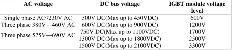
The rated voltage of the IGBT module is closely related to the input voltage of the APF. It is generally two times higher than the maximum value of the DC bus voltage. Table 1 lists the reference tables for selecting the voltage levels of IGBT module based on AC grid voltage or DC bus voltage.
TABLE I. REFERENCE TABLE FOR VOLTAGE RELATIONSHIP BETWEEN AC GRID VOLTAGE OR DC BUS VOLTAGE AND IGBT MODULE.
AC voltage DC bus voltage IGBT module voltage level
Single phase AC≤230V AC 300V DC(Max up to 450VDC) 600V
Three phase 380V―460V AC 600V DC(Max up to 900VDC) 1200V
Three phase 575V―690V AC 750V DC(Max up to 1100VDC) 1700V
1300V DC(Max up to 1800VDC) 2500V
[image:2.612.108.489.572.655.2]Rated Current of IGBT
IGBT is required to withstand higher switching frequency because that APF needs to compensate high frequency harmonic signal. Considering the current through IGBT and heat dissipation, there is an engineering empirical formula:
3 2 )
(
PF V
OL P
Peak I
ac
C (1)
Among them: P is design capacity, is the current ripple factor who is always
designed as 120%, OL is overload ratio who is value to 2 when design, Vac
represents the effective value of ac line voltage, PF is the power factor, is the output efficiency of APF and taken as 0.9 at design time.
According to the design capacity of APF and input voltage, we bring each
coefficient into formula (1), the peak current Ic of APF working well can be
obtained. Considering the impact of voltage and current when work, the parameter selection of IGBT should leave sufficient margin, so the rated current of IGBT
module should be selected to be 2-3 times the peak valueIc.
Switching Frequency Selection of APF
The selection of the frequency of the IGBT module should be based on thefrequency of the highest harmonic of the load current to be compensated. According to the sampling theorem, the switching frequency must be more than 2 times higher than that of the highest harmonic frequency. But in fact, when the frequency modulation ratio less than 7,the adjacent spectral valves will overlap and then result in obvious distortion of waveforms. If the APF is required to compensate the harmonics below 21, the operating frequency of IGBT should be greater than 7 *21 *50 Hz = 7350 Hz. Theoretically, the higher the switching frequency, the better the harmonic compensation effect of APF, and the smaller the volume of magnetic components. But with the increase of switching frequency, switching losses will increase, the requirements for heat dissipation when IGBT work will be higher, and also the price of IGBT devices. On the contrary, the lower switching frequency will lead to the lower compensation ability of APF for higher harmonics and the larger volume of magnetic components. Therefore, we should choose the appropriate switching frequency according to the harmonic compensation requirements of APF, the voltage level, current level and heat dissipation requirements of IGBT,and the cost of the main circuit. Then select different series of IGBT modules accordingly.
DESIGN OF DC SIDE VOLTAGE AND CAPACITOR CAPACITY
The function of the DC side capacitor is to provide DC voltage for the converter.
The DC side voltage Vdcshould be at least 1.5 times higher than the peak value of
the AC side phase voltage. DC-side voltage determines the compensating ability of APF. The greater the slope of maximum variation of total harmonic current, the higher the requirement of DCside voltage.
The DC side capacitor is an energy storage element and the energy is exchanged between load and APF. For nonlinear loads, the instantaneous power generated by harmonic current is not zero, but the average value of a period is zero. When APF compensates for harmonic currents, there is an energy exchange between the load and APF. So the DC side capacitor is required to provide a buffer for energy exchange. If the loss of APF is ignored, the DC side capacitor only absorbs and releases energy periodically. Therefore, the maximum energy △W exchanged between the load and APF is
s APF f P W
(2)
Among them,PAPFis the rated capacity for APF, fs is the switching frequency
of APF.
The energy of capacitor buffering can be expressed by the fluctuation of DC side
voltage. If the DC side voltage of APF is set as Vdc, and the fluctuation coefficient
of DC side voltage set as which is required not greater than 5%, there is the formula:
dc dc dc
dc dc
V V V
V
V ( )max ( )min
(3)
From the energy point of view, in aTs, the maximum energy exchange of the
APF is:
dc dc V CV W
(4)
According to formula (2), (3) and (4), the formula of capacitor can be obtained:
s dc APF
dc V f P V
W
C 2 2
In practical applications, the DC side voltage must be maintained basically unchanged to ensure the performance of APF. So the capacitive margin of DC side is usually larger because the DC side of APF is more concerned with stability.
PARAMETER DESIGN OF CONNECTING INDUCTOR
The connecting inductor is connected to the AC side power and the DC side capacitor. In a short switching period, the inductor determines the current rate of the main circuit when the voltage between the two ends of the inductor is determined. The greater the change rate, the faster the compensation speed, and the stronger the compensation ability, while on the contrary, the poorer the compensation capability. If the inductor is too large, its physical volume will be large which will make it bulky and expensive, and the current tracking speed will be slow. If the inductor is too small, the current ripple will be too large, which may cause the current to run out of control and destroy the switch device [7-9].
Therefore, L is a very important parameter, which directly affects the performance and controllability of APF. The inductor value of the inductor can be determined according to the formula[7] below.
max
9 4 9
4
I V L I f
V dc
s dc
(6)
Among them, Vdcis DC side voltage, fsis switching frequency of APF, ωis
fundamental frequency, Imaxand is amplitude of fundamental phase current, I is
output overshoot current.
When the DC side voltage is determined, the selection of L should be satisfied
with Lmin LLminon the basis of experiment. In this range, combined with control
strategy and modulation algorithm,compromised with the current response speed and current ripple, considered the price of inductor at the same time,then we can achieve the optimal configuration.
DESIGN EXAMPLES
Taking the APF of a 10kVA three-level four-leg main circuit as an example, the parameters of the APF main circuit are calculated and selected.The main technology requirements of the device is as follows. Its rated capacity is 10kVA, rated voltage is 90V / 50Hz, filterable harmonic number is 21 and below, and it also can suppress zero sequence current.
) ( 269 9 . 0 3 9 . 0 90 2 2 2 . 1 10000 3 2 P )
( APF A
PF V OL Peak I ac c
(7)
Considering the margin of 2-3 times, the IGBT module FF600R07ME4_B11 of Infineon is selected. Its voltage level is 600V and the working current is 600A.
The APF is designed to filter out the harmonics of 21 and below, so the switching frequency is selected as 10 KHz.
DC bus voltage should be greater than 1.5 times the peak voltage of AC side
voltage, so select 200VforVdc.
Bring each coefficient in formula (5), we can get:
F f V P C s dc APF
0.05 200 10000 500
10000
2
2
(8)
Considering a certain margin, we select C as 1000μF.For the main circuit of APF designed in this paper, the DC side capacitor is composed of two capacitors of equal size in series, so each capacitor should be 2000μF.
Bring each coefficient in formula (6), we can get:
H I f V L s
dc 165.22
2 . 0 269 10000 9 200 4 9 4
min
(9)
H I
V
L dc
9 2 50 269 1051.83 200
4 9
4
max
max
(10)
Select L as 800μH compromising.
EXPERIMENTAL RESULT
In order to verify the correctness of the parameter selection method proposed in this paper, an experimental platform is built, and the specific experimental parameters are as follows.
(1)The power line voltage is 90V/ 50Hz, and the system impedance is ignored. (2)The inlet inductor L of APF is 0.8mH, DC bus voltage Vdc is 200V, and the capacitor C is 2000μF.
(3)Three-phase uncontrollable rectifier load and one-phase uncontrollable rectifier load are selected for nonlinear load. Among them, the resistance is 16 and the inductor is 1mH.
Figure 2. Current of phase A before compensation.
Figure 3. Current of phase anafter compensation.
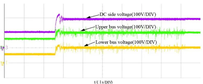
[image:7.612.102.491.468.630.2]Figure 2 is the voltage and current waveform of phase A before compensation. Figure 3 is the current waveform of phase a after compensation. According to the two graphs, the current distortion of phase A is serious before compensation, but basically sinusoidal after compensation. The compensation effect is very good. As shown in figure 4, the DC side bus voltage and neutral point potential are well controlled.The experimental results show that the main circuit parameter selection method can meet the design requirements.
CONCLUSIONS
According to the parameters selected in this paper, a prototype is built and the system experiment is carried out. The experimental results verify the feasibility of the main circuit parameter selection method used in the three-level four-leg APF system.
REFERENCES
1. Sumin Mao. June, 2009. Research on Three Phase Four Wire Shunt Active Power Filter [D]. Xu Zhou: China University of Mining and Technology.
2. Fang Zhuo, Yue Wang, Zhaoan Wang. 2001. Instantaneous Reactive Power and Active Power Filter in Three Phase Four Wire System [J]. Electrotechnical Journal, 2001(4): 1-4.
3. Aredes M., Watanabe E. H. 1995. New Control Algorithms for Series and Shunt Three-Phase Four-Wire Active Power Filters [J]. IEEE Trans. Power Delivery. 10(3): 1649-1656.
4. Jiuhe Wang, Jinlong Zhang, Huade Li. 2006. Design of Main Circuit Parameters for Direct Power Control System of Voltage Source PWM Rectifier [J]. Journal of University of Science and Technology Beijing. 11(28): 1091-1095.
5. Wenlong Qu, KeLiu. 1996. A Drive and Fast Protection Method for Large Capacity IGBT [J]. Journal of Tsinghua University, 36(5): 94-100.
6. Mei Tong, Ji Xiang. 2002. Variable Structure Control of a Hybrid Power Filter [J]. Transactions of China Electrotechnical Society, 17 (1): 59-63.
7. Jun Tao, Zhengzhi Liu. 2001. Design of Main Circuit Parameters for Active Power Filter [J]. Power Technology Application, 2001(3): 61-64.
8. Thomas T., Haddad K., Joos G. February 1996. Performance Evaluation of Three Phase Three and Four Wire Active Filter. Conference Record of the Industry Applications Conference. pp. 1016~1023.