WRL
Research Report 93/1
A Smart Frame Buffer
research relevant to the design and application of high performance scientific computers. We test our ideas by designing, building, and using real systems. The systems we build are research prototypes; they are not intended to become products.
There is a second research laboratory located in Palo Alto, the Systems Research Cen-ter (SRC). Other Digital research groups are located in Paris (PRL) and in Cambridge, Massachusetts (CRL).
Our research is directed towards mainstream high-performance computer systems. Our prototypes are intended to foreshadow the future computing environments used by many Digital customers. The long-term goal of WRL is to aid and accelerate the development of high-performance uni- and multi-processors. The research projects within WRL will address various aspects of high-performance computing.
We believe that significant advances in computer systems do not come from any single technological advance. Technologies, both hardware and software, do not all advance at the same pace. System design is the art of composing systems which use each level of technology in an appropriate balance. A major advance in overall system performance will require reexamination of all aspects of the system.
We do work in the design, fabrication and packaging of hardware; language processing and scaling issues in system software design; and the exploration of new applications areas that are opening up with the advent of higher performance systems. Researchers at WRL cooperate closely and move freely among the various levels of system design. This allows us to explore a wide range of tradeoffs to meet system goals.
We publish the results of our work in a variety of journals, conferences, research reports, and technical notes. This document is a research report. Research reports are normally accounts of completed research and may include material from earlier technical notes. We use technical notes for rapid distribution of technical material; usually this represents research in progress.
Research reports and technical notes may be ordered from us. You may mail your order to:
Technical Report Distribution
DEC Western Research Laboratory, WRL-2 250 University Avenue
Palo Alto, California 94301 USA
Reports and notes may also be ordered by electronic mail. Use one of the following addresses:
Digital E-net: DECWRL::WRL-TECHREPORTS
Internet: [email protected]
UUCP: decwrl!wrl-techreports
Joel McCormack
Western Research Laboratory
Bob McNamara
Smart Frame Buffer Group
January 1993
imized code size by including complex instruction decoding and operand fetch logic. As large caches became affordable, this complexity became a performance liability. Implementation issues like pipelining, memory latency, and multiple issue now drive instruction set design.
In turn, fast RISC processors have made simple graphics accelerators viable. When proces-sors were slow, high-performance graphics systems minimized processor intervention by includ-ing complex logic to parse graphics commands and to paint different shapes in a variety of pat-terns. For 2D graphics, at least, this complexity has become a performance liability. We believe that implementation issues like pipelining, memory organization and latency, and the exploita-tion of special video RAM funcexploita-tionality should now drive graphics accelerator design.
A dumb frame buffer is the ultimate in simplicity: graphics memory looks just like main memory. Reference [6] describes how we used this approach on early Digital RISC workstations to get cheap graphics with high performance. But processor, memory, and bus architectures limit dumb frame buffer performance: many processors implement byte writes as painfully slow read/modify/writes, and even fast I/O busses provide a small fraction of the bandwidth available from video RAMs. To fully exploit VRAM technology under these constraints requires special-ized graphics hardware.
The smart frame buffer is a small cheap gate array that locally expands 32 data bits into opera-tions upon 32 pixels; pixels can be 8, 16 or 32 bits deep. This expansion enables us to provide
1
information for 250 megapixels/second via the TURBOchannel bus. Different modes of opera-tion provide support for filling solid areas, stippling areas, copying areas, and drawing solid and dashed lines. Complex operations, such as computing the shape of an object and the pattern to paint within it, are left to the CPU.
Limiting graphics assistance to a few simple commands reduces chip cost, reduces design time, increases reliability, allows designers to focus upon making VRAM bandwidth available to the CPU, and allows graphics performance to improve in tandem with CPU performance.
The smart frame buffer design proved all of these advantages. Chip cost is less than the exter-nal glue logic it obviates. Initial design to power-up took 9 months. The chip contained two bugs, easily bypassed in software, and then fixed on the second pass. The full video RAM bandwidth is available to the CPU for most operations. And performance on many graphics
2
benchmarks has improved dramatically from the 25 MHz MIPS-based DECstation 5000/200 to the 150 MHz Alpha-based DEC 3000/500 AXP (Flamingo). The smart frame buffer sets an aggressive new level of performance for ‘‘low-end graphics,’’ and belies the common wisdom that graphics systems need to be complex to be competitive.
This paper describes the architecture of the smart frame buffer chip, sketches software 3
strategies for graphics operations common in the X Window System , and compares perfor-mance against other popular graphics hardware. Finally, we summarize the reasons why such simple hardware performs so well.
2. Design Goals and Strategies
In priority order, our design goals were time to market, cost, and performance. Performance improvements could not significantly impact an aggressive schedule, nor significantly increase cost over a dumb frame buffer system. We wanted to maximize the performance of our cheapest graphics systems.
To minimize design time, we kept things simple. All logic had to result in concrete perfor-mance improvements. We kept functionality as general as possible to allow extensive sharing of common logic among the different hardware modes, and to allow software to use these modes across a variety of painting algorithms.
To keep board manufacturing costs at or below that of a dumb frame buffer system, the gate array cost had to be offset by the elimination of random glue logic. The cheapest gate array available had too few pins for a 64-bit data path to video memory, so we settled for the next cheapest, with 184 I/O pins and 54,000 gates. We used 22,000 gates, which the manufacturer’s router could barely handle. We had enough pins and gates to implement the capabilities we really wanted, and no more. These constraints provided us with a technical excuse for avoiding additional capabilities that, while desirable, would have significantly lengthened the design time.
To get high performance, we carefully divided responsibility between the sfb chip and the CPU, so that each chip gets to do what it is best at. The gate array extracts the maximum pos-sible bandwidth from the video RAMs; the CPU implements painting algorithms.
Although many graphics accelerators include extensive control logic, we’d rather exploit the capabilities of CPUs than compete with them. The Alpha AXP CPU in a Flamingo workstation ticks at 6.7 nsec----nearly six times faster than our 40 nsec gate array clock----and faster CPUs are on the horizon. And by improving software painting algorithms, we can increase performance by without redesigning the graphics hardware.
2MIPS, R3000, and R4000 are trademarks of MIPS Technologies, Inc.
We use three strategies to maximize bandwidth and avoid reads and read/modify/write opera-tions over the TURBOchannel. The sfb chip is closely coupled to video memory with a wide data path, and implements semantics for planemasking and the Boolean combination of source and destination pixels. The sfb allows the processor to use 32-bit writes to word-aligned ad-dresses, and so avoid partial word writes that might not be supported by the CPU’s instruction set. Finally, all sfb operations complete within a bus timeout, so the processor never needs to check for overflow of the chip’s input buffer.
3. System Architecture and Interfaces
The primary external control functions of the smart frame buffer chip are to interface to the TURBOchannel I/O bus, to interface to the random-access and serial ports of the video RAM, to generate timing signals for the monitor, and to convert pixels to analog RGB composite video
4
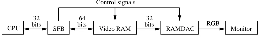
via a Brooktree RAMDAC. Figure 1 shows a block diagram of a complete graphics system built around the sfb.
CPU SFB
32 bits
64 bits
Video RAM
32 bits
RAMDAC Control signals
[image:7.612.102.548.290.356.2]Monitor RGB
Figure 1: Block diagram of primary sfb chip interfaces
The processor accesses the smart frame buffer via the TURBOchannel, a 32-bit shared data/address bus clocked at 40 nsec (25 MHz). Non-DMA writes take at least 120 nsec per 32-bit word, for a maximum transfer rate of 33 megabytes/second. Reads take at least 160 nsec, for a maximum rate of 25 megabytes/second. The sfb chip is a write-mostly device, and can accept 32 bits of data in the minimum 120 nsec bus write cycle. The processor reads data from the chip only to save sfb state when writing console messages, and to copy pixels from the screen into main memory. The sfb does not support DMA operations.
To increase bandwidth, the sfb uses a 64-bit interface to video RAM. As long as accesses stay within a 4096-pixel page, the chip can read or write 64 bits of data in 80 nsec. Access to a new page requires an extra 160 nsec, for a total of 240 nsec. Read/modify/write operations like xor require an additional 120 nsec, for a total of 200 nsec for accesses to the same page, and 360 nsec for accesses to a new page.
Video RAMs have a separate output port, fed by one of two large internal shift registers, for sending pixel data to the screen. Each half of a 4096-pixel page can be loaded into one of the shift registers in a few hundred nanoseconds by using a special memory transaction. When there is not enough data left in the shift registers to display the next scanline, the sfb loads one of the shift registers with the next 2048 pixels of data during horizontal blanking. The sfb sends data from the VRAM output port to the Brooktree RAMDAC, which converts the data to an RGB video signal.
4. Smart Frame Buffer Architecture
The smart frame buffer chip sits between the processor and video memory. The sfb chip operates in a 16 megabyte address space, as shown in figure 2. Most of the address space is devoted to frame buffer memory. The maximum frame buffer size is 8 megabytes, for use in a true color system with up to 1600x1280 32-bit pixels. Since the usual frame buffer size is 2 megabytes of 8-bit pixels, and since early workstations limited TURBOchannel address space, we alias portions of frame buffer memory to fit into smaller 4 and 8 megabyte address spaces.
Control registers 0 megabytes
2 megabytes
4 megabytes
8 megabytes
Alias to bottom 2
megabytes of frame buffer Alias to bottom 4
megabytes of frame buffer
8 megabytes of frame buffer
TURBOchannel ROM
SFB registers
RAMDAC registers
0 megabytes
1 megabyte
[image:8.612.55.515.177.402.2]1.75 megabytes
Figure 2: Address space of sfb chip
4.1. Dumb frame buffer mode
The sfb operates in several modes. In the simplest mode, the sfb acts like a dumb frame buffer. The processor can read or write a 32-bit word to any address in frame buffer memory. If the processor architecture supports byte or other partial word addressing, as do the MIPS R3000 and R4000, the processor can read or write any group of bytes within a 32-bit word.
4.2. Planemasking and Boolean functions
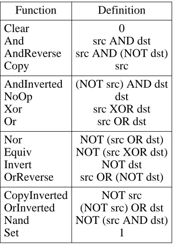
Dumb frame buffer mode and all the accelerated modes described below have hardware sup-port for a planemask and the 16 possible Boolean functions (‘‘rasterops’’) that combine source and destination pixels. These operations would otherwise require read/modify/write cycles in all but the simplest cases.
The X protocol allows a source pixel and a destination pixel to be combined using any of the 16 possible two-operand Boolean functions. The same graphics function applies to all bits in the pixels. Table 1 shows the name and definition of each graphics function.
Function Definition
Clear 0
And src AND dst
AndReverse src AND (NOT dst)
Copy src
AndInverted (NOT src) AND dst
NoOp dst
Xor src XOR dst
Or src OR dst
Nor NOT (src OR dst) Equiv NOT (src XOR dst)
Invert NOT dst
OrReverse src OR (NOT dst)
CopyInverted NOT src OrInverted (NOT src) OR dst Nand NOT (src AND dst)
[image:9.612.235.415.119.377.2]Set 1
Table 1: X11 graphics functions
The sfb chip implements all 16 Boolean functions in hardware. The sfb directly overwrites the destination pixels when using one of the four Boolean functions that do not depend upon the destination (Clear,Copy,CopyInverted, andSet). For the other twelve functions, the sfb reads the destination pixels, combines them appropriately with the source pixels, then writes the result back to video memory. These destination-dependent Boolean operations require an ad-ditional 120 nsec over the basic write cycle time, but this is much faster than forcing the proces-sor to read destination data over the bus, combine it with source data using logical operations, then write the result back over the bus.
4.3. Accelerated mode philosophy
A typical graphics accelerator accepts commands like ‘‘paint a rectangle,’’ ‘‘paint a triangle,’’ ‘‘paint text,’’ and ‘‘copy a rectangle.’’ The accelerator executes a sequence of microcode for each command. Each microcode routine computes the location of the object in video memory given its x and y coordinates, computes the shape of the object, clips the object to the window, figures out what data to fill the object with, and then issues a sequence of span filling operations to the most primitive layer of painting logic. (A span is a contiguous sequence of pixels on one scan line.) In many cases, the graphics accelerator chip is more complex and expensive than the processor chip to which it is attached!
For accelerated painting operations, the processor writes to a few sfb registers, like the foreground and background pixels and the mode register, then writes 32-bit data words into the frame buffer. Each write address is aligned to an 8-byte boundary, and tells the sfb where in the frame buffer to start painting. The write data tells the sfb what to paint. Each bit specifies what happens to one pixel, so a single data word may affect as many as 32 pixels. Different modes cause different interpretations of the 32-bit data word.
For a small increase in complexity over a dumb frame buffer, the sfb offers a large increase in performance by decreasing bus transactions, increasing available memory bandwidth, and free-ing the processor from low-level paintfree-ing operations.
Since the sfb maps one bit into a pixel, a system with 8-bit pixels reduces the number of bus transactions by 8 to 16 times. (Some operations in a dumb frame buffer require two transactions per word, thus the factor of 16.) This compaction in turn effectively increases the capacity of the processor’s write buffer.
The sfb can write eight 8-bit pixels every 80 nsec. To process a complete 32-bit data word, the sfb normally uses four cycles, or 320 nsec. For most operations, there are no idle cycles between 32-bit data words. Our measured write bandwidth is 93 megabytes/second----nearly three times the 32 megabytes/second we’ve measured over the TURBOchannel.
Finally, we get small-scale parallelism: while the sfb is processing one data word, the proces-sor can be computing the next word.
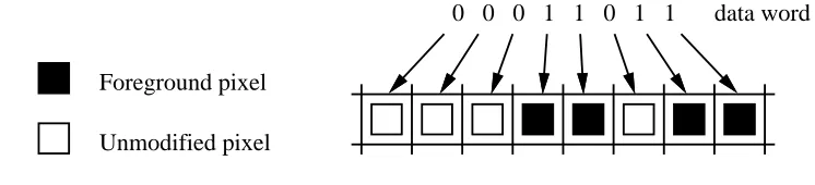
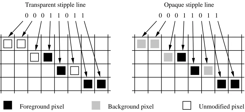
4.4. Transparent stipple mode
Transparent stipple mode expands 32 data bits to 32 pixels, with the following semantics:
•0 means do nothing
•1 means use the foreground pixel as the source pixel
Figure 3 shows a portion of a transparent stipple operation. Transparent stipple mode is used to fill areas with a single color, to fill areas in X11’s transparent stipple mode, to paint certain kinds of text, and to fill areas with certain tiles.
0 0 0 1 1 0 1 1
Foreground pixel
Unmodified pixel
[image:10.612.93.466.527.612.2]data word
Figure 3: Transparent stipple behavior
The sfb has a 32-bit foreground register, which must be loaded before using transparent stipple mode. Software replicates the foreground pixel to 32 bits on 8-bit and 16-bit pixel systems.
high-order bits at the right edge. To fill a span of less than 32 pixels, it zeroes the appropriate bits at both ends of the data word. The sfb hardware uses a priority encoder to skip over low-order zeroes, and stops painting when only zeroes remain in the high-low-order bits of a word.
Some graphics chips implement transparent stipple operations using read/modify/write cycles. The sfb avoids reads by using control logic on individual VRAM chips to disable writes to pixels with a 0 data bit. The theoretical peak fill rate is 8 bytes every 80 nsec, or 100 megabytes/second.
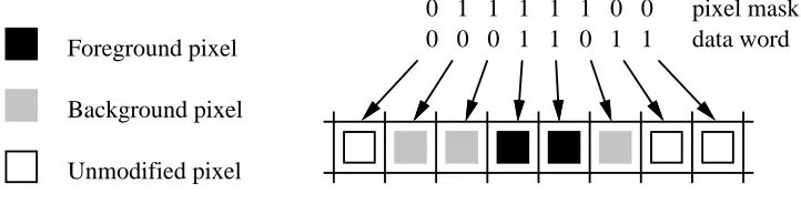
4.5. Opaque stipple mode
Opaque stipple mode expands 32 data bits to 32 pixels, with the following semantics:
•0 means use the background pixel as the source pixel
•1 means use the foreground pixel as the source pixel
Figure 4 shows a portion of an opaque stipple operation. Opaque stipple mode is used to fill areas with X11’s opaque stipple mode, to paint certain kinds of text, and to implement
CopyPlanerequests.
0 0 0 1 1 0 1 1 Foreground pixel
Background pixel
data word 0 1 1 1 1 1 0 0 pixel mask
[image:11.612.142.503.333.425.2]Unmodified pixel
Figure 4: Opaque stipple behavior
Like the foreground register, the background register is 32 bits wide. Both foreground and background must be loaded before using opaque stipple mode.
To fill narrow spans, or the left and right edges of longer spans, 0 bits in the data can’t be used as no-ops. The sfb provides a 32-bit pixel mask register: a 1 in the mask allows the correspond-ing pixel to be written, and a 0 prevents the pixel from becorrespond-ing written. To write less than 32 pixels in opaque stipple mode, the processor first writes to the pixel mask register, then writes a data word to the frame buffer. The pixel mask register resets to all 1’s after each use: most algorithms paint a scanline at a time, so this saves us from writing a mask of all 1’s to paint the middle of large spans.
4.6. Copy mode
When copying pixels from one area to another, the sfb cannot synthesize the source data from background and foreground pixels, but must read source data from memory. The sfb includes a 32-byte copy buffer for temporarily holding source data.
The processor transfers pixels in groups of 32 bytes by writing a pair of 32-bit data words. The processor first writes a data word to the address of the source pixels. A 1 in the data word indicates that the corresponding pixel should be read into the copy buffer, a 0 indicates that the pixel isn’t needed. The processor then writes a second data word, this time to the address of the destination pixels. A 1 in the data word indicates that the corresponding pixel in the copy buffer should be written, a 0 indicates that the destination pixel should be left unchanged.
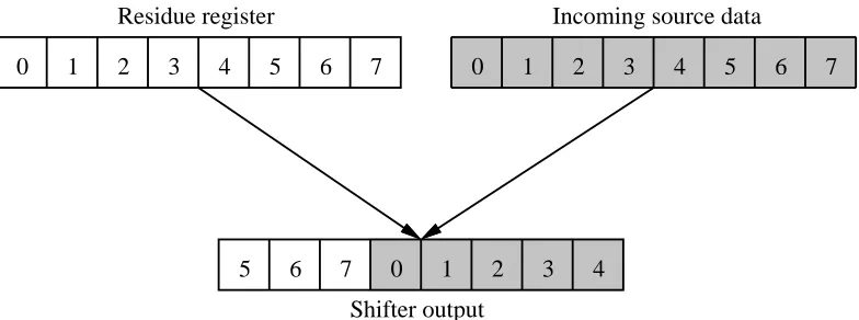
The sfb requires source and destination addresses to be aligned to 8 bytes, while an application can specify copies of arbitrary lengths that start at arbitrary byte addresses. If these byte ad-dresses are identical in the least significant three bits, as with a source address of 000216 and a destination address of 1002 , the processor can deal with the ragged edges by zeroing exactly16 the same bits in the source and destination masks. But what if the application’s source and destination addresses are misaligned with respect to each other? For example, the source address might be 000116while the destination address is 1004 . To support such unaligned copies, the16 sfb uses an 8-byte residue register and a shifter to assemble data from two consecutive 8-byte source words into an 8-byte destination word.
Before the sfb stores incoming source pixels into the copy buffer, it concatenates them with the residue register, then rotates this 16-byte result by -8 to +7 pixels. Backward (right-to-left) copies use rotations from -8 to -1, and forward (left-to-right) copies use rotations from 0 to 7. After extracting the destination word from the rotated result, the sfb moves the incoming data into the residue register, ready to be concatenated with the next 8 bytes of source data. The residue register maintains data between each 32-byte group of pixels, so that once an unaligned copy is started, each pair of data words copies a full 32 bytes of data.
In the example above, there is a 3-byte difference between the alignment of the destination address of 100416and the source address of 0001 . The processor loads this value into the sfb’s16 shift amount register before copying the scanline. As shown in figure 5, this causes the shift/residue logic to move the source data in byte 1 up to byte 4 in the destination.
Residue register
0 1 2 3 4 5 6 7
Incoming source data
0 1 2 3 4 5 6 7
Shifter output
[image:12.612.94.486.540.686.2]5 6 7 0 1 2 3 4
In the usual case, in which the source and destination addresses are on different VRAM pages, the copy logic has a theoretical maximum bandwidth of 33 megabytes/second.
The on-chip copy buffer is available to the processor as eight 32-bit registers. To transfer data from main memory to VRAM, the processor writes these registers, then writes a 32-bit data word to the destination address in the frame buffer. Conversely, to transfer data from VRAM to main memory, the processor writes a 32-bit data word to the source address in the frame buffer, then reads the copy buffer registers. The residue register and shift logic are enabled in both cases.
The sfb’s copy logic illustrates the advantages of keeping graphics hardware simple. We con-centrated on making the underlying copy functionality complete----supporting backward copies as efficiently as forward copies, and using the copy logic for transfers between main memory and VRAM----rather than putting higher-level control into hardware by supporting rectangle copies.
Implementing rectangle copies in hardware is a nightmare: overlapping rectangles may require copying from top to bottom or vice-versa, and from left to right or vice-versa, and source and destination addresses may not be aligned to VRAM words. In a vain attempt at simplification, some graphics chips read source data multiple times during unaligned copies. If the sfb took this approach, it would read 32 bytes, then write 24 bytes, slowing unaligned copy rates by 17%. Some chips support unaligned copies from left-to-right, but leave the backward direction to software! And even when a complex accelerator provides full rectangle copy support, it may have bugs----we know of one accelerator that can’t copy rectangles of width 1. Had this bug not been circumventable in software, another pass of the chip would have been required.
4.7. Line modes
Transparent and opaque stipple modes paint 32 pixels horizontally, and for long spans the processor must provide the starting address of each 32-pixel chunk. Transparent stipple and opaque stipple line modes differ from the span modes in that the sfb traces out a line that may go in any direction, it paints 16 pixels at a time, and it maintains the current address across 16-pixel chunks. Figure 6 shows a portion of transparent and opaque stipple line operations.
0 0 0 1 1 0 1 1 0 0 0 1 1 0 1 1
[image:13.612.115.538.496.689.2]Foreground pixel Background pixel Unmodified pixel Transparent stipple line Opaque stipple line
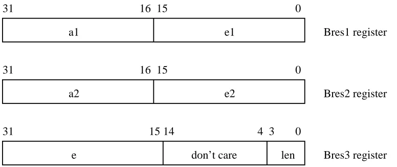
The sfb computes the path of a line through frame buffer memory using Bresenham’s algorithm [4]. The C equivalent of the hardware Bresenham step looks like:
*address = foreground; if (e < 0) {
address += a1; e += e1; } else {
address += a2; e -= e2; }
To paint a line, the processor provides initial values fore(a signed 17 bit number),e1ande2
(unsigned 16 bit numbers), a1 and a2 (signed 16-bit numbers), and the length of the line modulo 16 (a 16-bit pixel mask specifier would have required more CPU cycles and another bus write per line). The three line initialization registers are shown in figure 7.
31 16 15 0
a1 e1
31 16 15 0
a2 e2
Bres1 register
Bres2 register
31 15 14 0
e don’t care
4 3
[image:14.612.96.484.248.411.2]len Bres3 register
Figure 7: Line register formats
The processor then writes a data word to the starting address of the line, aligned to four bytes. The word contains up to 16 bits of transparent or opaque stipple line data, and the two low bits that were masked from the true starting address in order to align it. To paint longer lines, the processor writes as many additional 16-bit data words as necessary to a continuation register.
At the end of a line, the sfb leaves the address register one position past the last pixel painted. When painting lines that are connected end-to-end, this is the starting point of the next line. The processor thus avoids a multiply to compute the new starting address of each connected line.
The sfb doesn’t use 32 bits of line data for several reasons: there wouldn’t be room for the two low-order bits of address in the first data word, some lines would take longer than a bus timeout to paint if the graphics function required a read/modify/write cycle, and the X11 server’s dashed line code would have been much uglier.
The processor uses transparent stipple line mode for painting solid lines and dashed lines (al-ternating foreground with blank space), and opaque stipple line mode for double-dashed lines (alternating foreground and background). Since the processor explicitly provides stipple data for each line, dash patterns may be arbitrarily complex.
4.8. Support for processor idiosyncracies
Not all RISC processors are alike. We included a couple of capabilities----one intentional, one accidental----that avoid performance bottlenecks in the MIPS R3000 and the Alpha AXP 20164 CPU implementations.
The MIPS R4000 and Alpha AXP can map the entire frame buffer with a single special Trans-lation Lookaside Buffer entry. But the MIPS R3000 TLB effectively maps only 224 kbytes of memory. This is a small fraction of the screen memory; as the server draws objects on the screen, it often uses virtual addresses that are not mapped by the TLB. Even though the kernel usually requires only 17 instructions to load a new TLB entry, drawing lines to the dumb frame buffer caused enough TLB faults to significantly decreased performance.
We expected a large decrease in TLB faulting overhead using the sfb, as the processor writes to the frame buffer once per line rather than once per pixel. Early performance simulations proved us wrong. While the decrease in TLB misses per line helped, we were painting lines more quickly, and so TLB faults still occured about as frequently per second for 10-pixel lines.
When we modified the line-drawing hardware to leave the address in the right place at the end of a line, the TLB problem mostly disappeared for connected lines as a side effect. The new code wrote to the frame buffer once perPolylinerequest, rather than once per line.
For unconnected lines, we added an address register and a ‘‘start’’ register. Instead of writing a data word directly to the frame buffer, the processor can first write the address to the address register, then write the data to the start register. The TLB usually contains a page entry for the sfb registers, so these two transactions rarely cause a TLB fault. During performance tuning, we found that using the address register also sped up painting of small rectangles and spans.
The Alpha AXP architecture was designed to support fast memory system interfaces. There are no guarantees that reads and writes will be issued in the order that they occur, or that they will even be issued if they are redundant and can be eliminated. This creates problems for memory-mapped I/O devices like the sfb. For example, if the CPU’s write buffer rearranges the order of writes while the sfb is in copy mode, the source becomes the destination and vice-versa.
The Memory Barrier instruction separates memory transactions. All memory transactions ex-ecuted before the MB instruction must complete their accesses to memory before any actions executed after the MB instruction can access memory. To keep a series of memory trans-actions in order, the programmer must include an MB instruction between each access.
Memory Barrier semantics require it to act only as a separator between memory accesses, but the existing Alpha chip brings the processor to a grinding halt, flushes the CPU write buffer, signals the external memory system, and waits for a reply. On the Flamingo workstation, this involves tens of nanoseconds, or somewhere in the neighborhood of 6 to 12 instruction cycles.
In the meantime, we exploit ‘‘don’t cares’’ in the sfb’s address decoding, which uses high-order bits to determine that the processor is accessing a register, and low-high-order bits to determine which register. It ignores the mid-order bits, so the entire register set is aliased many times at 128-byte intervals.
The Flamingo server uses this aliasing to avoid Memory Barrier instructions. It cycles through eight aliased sets of registers; moving from one aliased set to the next requires two in-structions. The aliases put enough distance between register addresses to prevent the write buff-er from reordbuff-ering or eliminating registbuff-er accesses. We latbuff-er discovbuff-ered that we could alias the frame buffer in a similar way. Register and frame buffer aliasing eliminated about 95% of the Memory Barrier instructions previously required.
5. Smart Frame Buffer Configurability
The sfb chip can be used to implement a wide range of graphics systems. It offers multiple pixel depths, a cornucopia of screen resolutions and refresh rates, memory configurations from two to eight megabytes, and can be attached to one or two screens.
5.1. Pixel depths
The smart frame buffer supports pixel depths of 8, 16, and 32 bits. Physical pixel depth is fixed for a given graphics board, as memory must be wired slightly differently in each case. Some Brooktree RAMDACs support the appearance of different depths by allowing control bits in each pixel to specify how the rest of the bits should be interpreted.
The 8 bits per pixel graphics system uses the Brooktree 459 RAMDAC, which has a 256-entry colormap. Each entry in the colormap contains 8 bits each of red, green, and blue intensity data.
A 16 bits per pixel graphics system would use the Brooktree 463 RAMDAC, configured on a per-pixel basis to use 4 bits each of red, green, and blue intensity data directly from the pixel, or to use 8 bits of the pixel as an index into one of two 256-entry colormaps. This system would support two bits of overlay planes that are displayed ‘‘on top’’ of normal pixel data.
A 32 bits per pixel graphic system would also use the Brooktree 463. This system could display 8 bits each of red, blue, and green directly from the pixel, or use 8 bits of the pixel as an index into one of two 256-entry colormaps. This system would support 4 bits of overlay planes.
Increasing pixel depth decreases bandwidth as measured in pixels per second. In one 80 nsec cycle, the sfb can paint eight 8-bit pixels, four 16-bit pixels, or two 32-bit pixels. This reduction in bandwidth mostly affects large area fills and copies; small area, line, and text performance are governed by other factors, and so don’t slow down in direct proportion to pixel depth.
In 16-bit and 32-bit pixel systems, the sfb may not paint a full 32 pixels for each 32-bit data word. The sfb uses an 8-input priority encoder to skip over low-order groups of 0 bits in the pixel mask. But when using 32-bit pixels, a data word contains 16 groups of two bits, and opaque and transparent stipple modes use only the bottom 16 bits of the data word.
5.2. Monitor resolutions and refresh rates
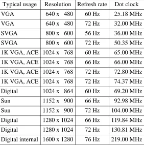
Digital sells monitors offering resolutions from 640x480 to 1280x1024, using refresh rates from 56 Hz to 76 Hz. We wanted to support all these monitors, and any likely new candidates, so we made the sfb monitor timing generation logic fully programmable.
The sfb uses an external pixel dot clock to generate timing signals for the RAMDAC and video RAMs; this clock’s frequency is specific to the monitor’s resolution and refresh rate. Programmable clocks were noticably inferior to fixed frequency crystals in image clarity; we suspect this was due to minor instabilities in the clock period. We turned the disadvantage of using a different crystal for each type of monitor into a user-friendly feature. We use the dot clock frequency, rather than board jumpers or switches, to automatically determine screen resolution and refresh rate. We support all Digital monitors and most of our competitor’s as well, as shown in Table 2.
Typical usage Resolution Refresh rate Dot clock
VGA 640 x 480 60 Hz 25.18 MHz
VGA 640 x 480 72 Hz 32.00 MHz
SVGA 800 x 600 56 Hz 36.00 MHz
SVGA 800 x 600 72 Hz 50.35 MHz
1K VGA, ACE 1024 x 768 60 Hz 65.00 MHz
1K VGA, ACE 1024 x 768 66 Hz 66.00 MHz
1K VGA, ACE 1024 x 768 72 Hz 72.80 MHz
1K VGA, ACE 1024 x 768 72 Hz 74.37 MHz
Digital 1024 x 864 60 Hz 69.20 MHz
Sun 1152 x 900 66 Hz 92.98 MHz
Sun 1152 x 900 72 Hz 104.00 MHz
Digital 1280 x 1024 66 Hz 119.84 MHz
Digital 1280 x 1024 72 Hz 130.81 MHz
[image:17.612.184.466.257.540.2]Digital internal 1600 x 1280 76 Hz 219.00 MHz
Table 2: Preprogrammed monitor resolutions and refresh rates
5.3. Memory configurations
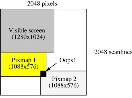
Many graphics accelerators convert an object’s x and y coordinates to a frame buffer address. This involves multiplying the y coordinate by the scanline stride (which may be wider than the visible screen width). These accelerators often restrict the stride to an easy multiplier constant like 1024, 1280, or 2048. Since all pixmaps must use this same stride, software must use a complex and wasteful two-dimensional allocator. Figure 8 shows a 1280x1024 screen with a stride of 2048 bytes embedded within four megabytes of memory. The two 1088x576 pixmaps require a total of 1.2 megabytes, but they can’t both fit into the available 2.75 megabytes of off-screen memory.
Visible screen (1280x1024)
Pixmap 1 (1088x576)
Pixmap 2 (1088x576)
Oops! 2048 pixels
[image:18.612.173.400.209.377.2]2048 scanlines
Figure 8: A two-dimensional allocator wastes space
The sfb leaves computation of an object’s address to the processor, and packs screen scanlines end-to-end in video memory regardless of screen resolution. The sfb requires only that screen and pixmap rows be padded to a multiple of 64 bits, which allows software to use a simple and efficient one-dimensional memory allocator for off-screen pixmaps.
Using 256k by 4-bit parts, the minimum memory configuration requires 16 VRAM chips for a total of 2 megabytes. The standard 8-bit 1280x1024 screen uses 1.25 megabytes of video memory. The remaining .75 megabyte is available for off-screen pixmaps. The sfb-based HX graphics board has space for an additional 2 megabytes of DRAM, although this configuration is not supported as a product. The X server uses this memory for pixmaps; a four megabyte board has ample memory for full-screen double-buffering applications.
A 16-bit pixel system requires 4 megabytes, or 8 megabytes for full-screen double-buffering. A 32-bit pixel system requires 8 megabytes of memory, which is the maximum allowed, and so full-screen double-buffering isn’t possible.
5.4. Multiple monitors
6. Software Algorithms
The sfb-specific X server code borrows heavily from the dumb frame buffer code described in reference [6]. We use the dumb frame buffer code to paint to pixmaps that reside in main memory, so we don’t have to limit pixmaps to off-screen video memory. We also used this code as a template for sfb-specific code; in many routines the only significant changes were in the low-level span filling loops. By recycling cfb code, we took just two months to create an X11 server that exercised the sfb software simulator.
The sfb-specific server code is 16,100 lines of C and 850 lines of MIPS assembler, which generates 116,000 bytes of object code. This compares quite favorably to the dumb color frame buffer code, which is 13,200 lines of C and 3,300 lines of assembler, generating 262,000 bytes of object code. (Many of the dumb cfb files are compiled three times in order to implement all 16 Boolean graphics functions, hence the much larger object code size.)
6.1. Directory structure and parameterization
The MIT X server [2, 3] lets programmers add support for new graphics devices with minimal impact on the rest of the server. We modified a few cfb routines so that the sfb code could call them, and changed some initialization code to recognize the smart frame buffer. Otherwise, all support for the sfb is confined to the three device-dependent X directories sfb, sfb16, and
sfb32.
In order to maintain one set of sources for all pixel depths, we parameterized as much as we could in a few header files, and resorted to about 50 C #ifdef preprocessor statements else-where. All source files reside in thesfbdirectory; thesfb16andsfb32directories use sym-bolic links to the sources insfb. The main definition file for sfb functionality,sfb.h, includes another file sfbparams.h. This file is in turn a symbolic link to an actual parameterization file: insfbit points to a parameter file appropriate for 8-bit pixels, insfb16to a file for 16-bit pixels, and insfb32to a file for 32-bit pixels.
Each actual parameterization file contains six definitions:
sfb sfb16 sfb32 #define SFBPIXELBITS 8 16 32 #define SFBSTIPPLEBITS 32 32 16 #define SFBCOPYBITS 32 16 8 #define SFBLINEBITS 16 16 16 #define SFBBUSBITS 32 32 32 #define SFBVRAMBITS 64 64 64
SFBPIXELBITSdefines the number of bits per pixel. SFBSTIPPLEBITSdefines the num-ber of bits in a data word that the sfb uses in transparent and opaque stipple modes.
SFBCOPYBITS defines the number of bits in a data word that the sfb uses in copy mode.
SFBLINEBITS defines the number of bits in a data word that the sfb uses in transparent and opaque stipple line modes. SFBBUSBITSdefines the number of data bits in the TURBOchan-nel bus. FinallySFBVRAMBITSdefines the number of bits in the sfb interface to video RAM.
6.2. Solid area filling
The simplest operation in an accelerated mode is solid area filling; the example in figure 9 shows the basic techniques of mask generation used throughout the sfb code. This code assumes that the planemask and foreground color have already been loaded, that the mode has been set to transparent stipple, and that the span has been clipped to the window boundaries.
/* Compute starting address of span within frame buffer */ p = pdstBase + y*drawableWidth + x*SFBPIXELBYTES;
/* Compute how many bytes past 8-byte alignment */ align = (int)p & SFBALIGNMASK;
/* Align starting address to 8-byte alignment */ p -= align;
/* Convert align from number of bytes to number of pixels */ align /= SFBPIXELBYTES;
/* Add the number of alignment pixels to the total width */ width += align;
/* Compute a left mask with low 0’s where alignment was */ needed */ leftMask = SFBSTIPPLEALL1 << align;
/* Compute a right mask with high 0’s past the (extended) */ width */ rightMask = SFBSTIPPLEALL1 >> (-width & SFBSTIPPLEBITMASK); if (width <= SFBSTIPPLEBITS) {
/* Mask fits into a single word */ SFBADDRESS(sfb, p); /* Minimize TLB misses */ SFBSTART(sfb, leftMask & rightMask);
} else {
/* Mask requires 2 or more words */ SFBWRITE(p, leftMask);
width -= 2*SFBSTIPPLEBITS; while (width > 0) {
p += SFBSTIPPLEBYTESDONE; SFBWRITE(p, SFBSTIPPLEALL1); width -= SFBSTIPPLEBITS; }
SFBWRITE(p+SFBSTIPPLEBYTESDONE, rightMask); }
Figure 9: Solid filling prototype code
Ifp= 100516andwidth= 9, the code computes the following masks:
leftMask 11111111 11111111 11111111 11100000 rightMask 00000000 00000000 00111111 11111111 leftMask & rightMask 00000000 00000000 00111111 11100000
To paint a rectangle, the processor first computes masks and a starting address, then branches into a loop for narrow rectangles that can be painted with one data word, or a loop for wider rectangles that require two or more data words.
6.3. Transparent stipples, opaque stipples, and tiles
The X server uses the solid area code as a template for the routines that paint certain stipples and tiles. Stipples are bitmaps that are expanded using transparent or opaque stipple semantics, while tiles are pixmaps that are copied. The bitmap or pixmap pattern is repeated both horizon-tally and vertically in order to fill areas larger than the pattern.
Stipple data is often provided in a bitmap with a width that is a power of 2, like 8, 16, or 32. Tile data is often provided in a pixmap with a width of four pixels, or 32 bits on an 8-bit pixel system. The sfb code replicates any such bitmap or pixmap to a width of 32 bits, and provides special routines for painting these patterns. These special cases of stipple and tile painting are so similar that the same source code is compiled three times, with a few #ifdef statements to implement the differences.
In the transparent and opaque stipple code, the processor fetches a 32-bit word from the ap-propriate row of the bitmap, rotates this word based upon the position in the window, then writes the rotated data every 32 pixels across the entire span (masking off a few bits at the edges).
The tile code rotates data on pixel boundaries rather than on bit boundaries, then loads the foreground register with the rotated data. The foreground register is 32 bits wide, so it can hold a different 8-bit pixel value in each byte. The server then fills the span as if it were filling a solid area. Though this code can paint tiles that are no wider than four pixels on an 8-bit pixel system,
5
this is often sufficient. For example, the Display PostScript System [5, 1] uses a tile four pixels wide by six pixels high for color half-toning.
Stipples of widths that are not a power of two are uncommon, so the server code for them is fairly inefficient. The server fetches either a full 32-bit word, or whatever is left of the stipple, then paints this data word. To satisfy alignment constraints, the server usually has to paint the data word in two operations; in opaque stipple mode this also requires two writes to the pixel mask register.
The server uses code similar to that described below for copies in order to fill areas with tiles that are larger than 32 bits in width.
6.4. CopyPlane
TheCopyPlane operation looks like a non-repeated opaque stipple of arbitrary size. These requests are common enough that the server has special code for large bitmap patterns. Since
CopyPlane doesn’t involve the complications of repeating the bitmap pattern, its inner loop arranges data in order to extract maximum bandwidth from the sfb. This loop maintains the unused bits from the previous iteration, fetches one new 32-bit word, shifts and merges these two
words, then writes the resulting data word directly to an 8-byte aligned address. In the middle of a span, each 32 pixels require a single write to the sfb, rather than the four writes used by the general opaque stippling code.
6.5. Copies
Copy code is an obvious extension of theCopyPlane code, in which the source bitmap be-comes a pixmap. Copies involve two independent frame buffer addresses----source and destination----which may not be aligned. The processor must write the shift amount to the sfb, and may need to prime the shift/residue logic at the beginning of a span, and drain the logic at the end of a span.
If the alignment of the source address is larger than the destination alignment, the first 8-byte word from the (alignment-adjusted) source address may not contain enough data to write to the first 8-byte word of the (alignment-adjusted) destination address. Figure 10 shows a copy of 7 bytes where the source alignment is 2 and the destination alignment is 1.
0 1 2 3 4 5 6 7
2 3 4 5 6 7 Source
Destination . . .
8 9
[image:22.612.125.442.293.372.2]0 1
Figure 10: A copy that requires priming the shift/residue logic
In this case, the processor backs up the aligned destination pointer by an additional 8 bytes, and shifts 0’s into the bottom 8 bits of the left edge destination mask, so that the sfb loads the first 8 bytes of the source into the residue register without writing anything to the destination.
[image:22.612.124.453.524.601.2]Similarly, the processor may need to drain data from the residue register at the end of the span. Figure 11 shows a copy of 6 bytes where a single 8-byte source word contains data that must be written to two different 8-byte destination words. We read an extra 8-byte word after the source to force pixels through the shift/residue logic.
0 1 2 3 4 5 6 7
0 1 2 3 4 5 6 7 Source
Destination 8 9 . . .
Figure 11: A copy that requires draining the shift/residue logic
6.6. Text
X11 has two types of text painting requests. PolyText paints a string of characters using transparent stipple semantics to spatter foreground pixels onto the destination. ImageText
paints a string of characters using opaque stipple semantics to fill in the area around characters with the background pixel.
In a fixed-metric font, each glyph (bitmap picture of a character) is the same height and width. In a variable-pitch font, glyphs can be different heights and widths. The server uses different strategies to paint variable-pitch and fixed-metric fonts.
The PolyText code for variable-pitch fonts uses transparent stipple mode in an obvious fashion. It looks up the bitmap glyph for each character in the string, and paints one glyph at a time from the top row to the bottom. The corresponding ImageTextcode doesn’t use opaque stipple mode, because painting background and foreground simultaneously in these fonts is hard: each glyph must be extended up and down to the overall font height, the space between glyphs must be filled in, and in some fonts information from two adjacent glyphs can overlap (as with an overstrike character). The server avoids these problems by clearing a rectangle of the ap-propriate size with the background pixel, then calling thePolyTextcode.
ThePolyTextandImageTextcode for fixed-metric fonts share the same source file, with a few#ifdefsto handle masking correctly. Since all glyphs are the same height and width, it is easy to merge information from the same row of several adjacent glyphs.
Our original code painted glyphs one at a time up to the first 8-byte aligned address, painted the middle of the string with full 32-bit data words assembled from multiple glyphs, then finally painted the last few glyphs one at a time. Performance was disappointing. We were nowhere near saturating TURBOchannel or sfb memory bandwidth anyway, and so the effort expended to use only aligned, 32-bit writes in the middle of the string was in vain.
We improved performance with a simpler algorithm. The processor paints glyphs in groups that are guaranteed to fit into a 32-bit data word, regardless of alignment constraints. For ex-ample, if each glyph is 6 bits wide, the processor can fit data from four glyphs into a 32-bit data word, and still have room to shift the data left as much as 7 bits in order to satisfy the 8-byte alignment constraint. Similarly, the processor can fit data from three 8-bit wide glyphs into a data word, and still have room to shift the data to satisfy alignment constraints. Our new code writes to the sfb more often, but uses many fewer CPU cycles.
6.7. Lines
Though largely irrelevant for most 2D applications, the most commonly quoted graphics per-formance benchmark is 10-pixel lines. Not coincidentally, line painting is the only area where we descended into assembly code and literally counted every instruction. We maximized perfor-mance by avoiding data shuffling and masking, by using fast clipping code, and by using posi-tion within code rather than data registers to record important decisions.
Referring back to figure 7, note that signed fields are in the most significant bits of registers so that the processor doesn’t need to zero sign bits of negative values. We also pushed eas far as possible from the len field. The maximum line length we allow is a 15-bit unsigned number; we don’t explicitly zero the high 11 bits, as the sfb ignores them. Our arrangement of fields saves three instructions over a more careless layout. This seems insignificant, but removing a single instruction increases 10-pixel line performance by 0.4% to 1.9% on various DEC worksta-tions. If you take care of the nanoseconds, thex11perfresults will take care of themselves.
We avoid shifts by computing a1anda2in the high 16 bits of the CPU registers. The com-putation of e requires a divide by 2, but we just shift left by 14 bits rather than 15; as with the length field, the unused bottom bit is ignored. Avoiding shifts saves another three instructions.
To determine if a line is completely visible within a window, we borrowed Keith Packard’s code from the MIT X11R5 sample server. This code simultaneously compares 16-bit x and y coordinates in a single 32-bit subtract. Testing unconnected lines for visibility requires 11 in-structions. The connected line code remembers visibility status of the ending point, which be-comes the starting point of the next line. If this point is known to be visible (the usual case), testing the new end point uses only 8 instructions.
Finally, rather than painting all lines with the same loop, our code branches into one of four cases depending on whether the line is more horizontal than vertical, and whether the line goes forward or backward. This reduces line overhead by a few more instructions.
7. Design Style and Simulation
Joel McCormack works in Palo Alto, California. Bob McNamara works in Maynard, Mas-sachussetts. Bob visited California once to discuss the original sfb proposal, which was no more than a page of rough ideas. Joel visited Massachussetts once when we powered on the sfb-based HX board. We used the phone to discuss ideas, electronic mail to keep a written record of our decisions, and a behavioral simulator to act as the final authority on the chip’s functionality.
Using the phone instead of a whiteboard sometimes resulted in the two of us believing our-selves to be in agreement on an issue, whereas in reality we were talking about entirely different strategies. Since we could ultimately discover and resolve misunderstandings with the simulator, this ambiguity turned out to be a benefit. It allowed us to agree upon a set of goals, and then independently explore alternatives to accomplish those goals. Eventually (and usually inadver-tently), we would discover just how different our approaches were, discuss the strengths and weaknesses of each, and then choose one.
We used electronic mail primarily as a written record of important design decisions made during telephone calls, and to write up extensive performance computations. We also used mail to send an English specification of the chip back and forth, but this specification was imprecise and usually out of date.
The true specification of the chip was the behavioral simulator. The simulator consisted of a few C source files written by Bob McNamara and Lindsay Gage. Programs call the simulator’s
Bob and Lindsay used the simulator to create simple test cases for the chip. Their program parses a file of drawing commands, then translates these into BusWrite calls to the sfb registers and frame buffer. Their do_rams routine writes pixels to an X window to show the result of the commands. In many graphics chip designs, this is where the use of the simulator ends.
Joel McCormack wrote and debugged X server code for the chip by linking the simulator into an X server. This server communicates with the sfb hardware via conditionally compiled macros that either directly read and write the memory-mapped registers and frame buffer, or call the simulator’s BusRead and BusWrite procedures. His do_rams routine writes pixels to a dumb color frame buffer graphics card, turning it into a (very slow) sfb display.
The simulator allowed development of server code before the chip was ready, and yielded more subtle advantages as well. Regardless of the state of the document and the ambiguities of its English prose, the simulator provided an ironclad contract between hardware and software. If the simulator performed a certain function, the chip was expected to perform that function in exactly the same manner. The simulator provided feedback on our design: as we converted painting routines to use the smart frame buffer, we altered the chip architecture to better suit our needs. And the simulated server uncovered a few subtle bugs in the hardware design that had been missed by the simpler test cases.
Finally, the simulator allowed us to efficiently and comprehensively verify the schematic diagrams used to fabricate the chip. Joel used the sfb server to run every X program he could find, recording both the commands that the server sent to the simulator, and the video memory transactions that the sfb sent in response. This resulted in hundreds of megabytes of trace data, painfully gathered over a few weeks.
When the schematics were complete, Bob wrote a program to translate the schematics into a gate-level simulator, which ran seven times slower than the high-level behavioral simulator. This was too slow for interactive use, but fast enough to run the command traces gathered with the high-level simulator and check that the two simulators issued exactly the same memory transactions. To speed this process we checked several traces simultaneously using multiple workstations.
Trace verification revealed several areas where the schematics did not match the high-level C simulator code, as well as some timing problems. When the gate-level simulator could run all traces without error, we sent the schematics to the gate array vendor to be placed and routed.
Subsequent testing revealed an insignificant hardware error in lines, which hadn’t been tested by the server due to an unclosed comment in some C code. We also discovered a race condition in the copy logic, but soon relabeled this a ‘‘performance enhancement.’’ Fixing the race con-dition in hardware would require adding an extra 40 nsec clock tick to all copy requests; fixing it in software required two extra lines of setup when copying narrow rectangles.
We discovered a few bugs in the X server software when we reran the set of test programs used to provide traces. The simulator was so slow that it hadn’t allowed us to completely ex-ercise some real-time X applications.
Nonetheless, within a couple weeks of power-on, several of us were using the sfb boards and X server for our daily work. At this point, we concentrated almost entirely upon performance tuning rather than debugging. This would not have been possible without the extensive simula-tions conducted before the chip was taped out.
8. Performance Measurements
Quoting theoretical ‘‘speed-of-light’’ graphics hardware capabilities is a common but mislead-ing practice, rivallmislead-ing the use of ‘‘peak MIPS’’ in optimistic uselessness. The theoretical num-bers we have provided above show hardware performance limits; the numnum-bers below show how closely we have come to achieving those limits in practice.
We use the x11perf program to measure X11 server performance. While this benchmark reports performance numbers higher than most applications will attain (its painting requests con-tain as many as 1000 objects), it is an actual application painting with X graphics requests. Since alternate X servers (such as those available from MIT’s X Consortium) may outperform a vendor’s server on some tests, we always use the highest x11perf numbers available for a given workstation.
CPU horsepower and the mechanism used to transport data from the application to the X serv-er have a big impact upon pserv-erformance, so we compare sevserv-eral sets of sfb pserv-erformance numbserv-ers with performance results from Sun and Hewlett-Packard machines. We have attempted to match the sfb configurations as closely as possible to the other vendors’ configurations.
The dumb color frame buffer numbers were generated using the sfb in simple dumb frame buffer mode, and show what performance is possible with no hardware help. In many cases these numbers are limited by TURBOchannel bandwidth, and would be higher if graphics memory were more tightly coupled to the processor.
The Sun results are from a SPARCstation 2 with a GX graphics accelerator [7]. This con-figuration has CPU performance comparable to a DECstation 5000/200. Using the 1992 SPECint benchmarks, the SPARCstation rates about 22 integer SPECmarks, the DECstation
6
about 20. Both use UNIX sockets for communication between the application and the X server.
The GX graphics accelerator [7] qualifies as complex. It has three drawing functions: draw a point/line/triangle/quadrilateral filled with any 16x16 transparent or opaque stipple pattern; copy
a rectangle; and draw text. The GX computes a starting addresses in the frame buffer given an object’s x and y coordinates. It clips objects against two rectangles. If an object is partially outside of the soft clip rectangle, the GX computes values for all pixels in the object, but doesn’t actually paint the pixels that are clipped. If an object is partially outside of the hard clip rec-tangle, the GX doesn’t paint anything, but notifies the processor so that it can clip the object in software. Internally, it uses a massively parallel state machine (‘‘SuperCISC’’).
Many features of the GX interact poorly with X11 or the I/O bus. The GX’s internal coor-dinate system system is 14 bits, but X11 uses 16 bits; large X11 coorcoor-dinates that should be clipped alias into coordinates that the GX considers visible. These 14-bit values each require a separate 32-bit write; packing two to a word would reduce bus traffic and increase command buffer capacity. The processor cannot stream commands to the GX, but must constantly ask if there is room in the command buffer and whether an object is contained in the hard clip rec-tangle. The GX line hardware always paints the last endpoint, which makes it inefficient on all
Polylineand somePolySegmentrequests.
The DECstation 5000/240 and the Alpha-based Flamingo workstation bracket the HP 730’s CPU performance. The DECstation 5000/240 rates about 27 integer SPECmarks, the HP 730 about 48, and the Flamingo about 74. Many of the Flamingo performance numbers below are preliminary, and may improve with better compiler technology and with server performance tuning. All three systems use shared memory for communication between an application and the X server.
HP has published nothing specific about their CRX graphics board, and so we know almost nothing about its organization and capabilities.
8.1. Rectangle performance
Painting something as simple as a rectangle requires a good deal of software for the sfb. The server must clip the rectangle to the window, compute a starting address, compute left and right edge masks, and write at least one data word per scanline. If the rectangle is stippled, the server must also fetch the stipple pattern for each scanline. The Sun GX performs all these operations in hardware given the four corners of the rectangle.
Benchmark DEC Sun DEC DEC HP DEC
(kilorectangles/sec) 5000/200 SS2 5000/200 5000/240 730 Flamingo w/cfb w/GX w/sfb w/sfb w/CRX w/sfb
Solid 10x10 92 150 156 229 280 423
Transparent 10x10 34 150 96 166 126 448
Opaque 10x10 32 150 96 141 126 299
[image:27.612.123.528.522.645.2]Tile 10x10 38 150 93 137 130 359
Table 3: Small rectangle fill performance
when the CPU must execute stipple fetching code. This handicap disappears with more CPU power, and an sfb on a Flamingo easily outdistances both the GX and the CRX. The Flamingo fills solid 10x10 rectangles at 95% of the sfb’s theoretical maximum of 444,000 rectangles/second.
Setup times are insignificant for large rectangles; the tests shown in Table 4 measure raw bandwidth. The HP CRX provides an impressive solid fill rate, but this is not sustained in the other fill modes. The largeCopyPlanerequest shows how fast each graphics system can paint an opaque stipple when the source bitmap is large, and thus cannot be loaded once per scanline or once per window.
Benchmark DEC Sun DEC DEC HP DEC
(megabytes/sec) 5000/200 SS2 5000/200 5000/240 730 Flamingo w/cfb w/GX w/sfb w/sfb w/CRX w/sfb
Solid 500x500 30 98 90 91 109 94
Transparent 500x500 14 98 90 91 69 94
Opaque 500x500 25 98 85 86 69 91
Tile 500x500 22 97 90 89 69 93
[image:28.612.83.496.214.356.2]CopyPlane 500x500 15 50 67 79 65 88
Table 4: Large rectangle fill performance
8.2. Copy performance
A single X11 rectangle fill request can contain coordinates for thousands of rectangles, but a copy request contains coordinates for exactly one source and destination rectangle pair; small rectangle copies involve so much overhead that they reveal little about accelerator hardware. The large rectangle times in Table 5 show raw copy bandwidth.
Benchmark DEC Sun DEC DEC HP DEC
(megabytes/second) 5000/200 SS2 5000/200 5000/240 730 Flamingo w/cfb w/GX w/sfb w/sfb w/CRX w/sfb
Screen to screen 5 18 32 32 40 32
Main to screen 10 9 12 13 40 27
Screen to main 6 4 6 6 5 8
Main to main 11 11 11 12 22 81
PutImage 2.3 1.6 2.9 6.0 9.4 12.0
Table 5: Rectangle copy performance
[image:28.612.85.492.474.618.2]Main memory to screen copies usually occur when an application requests that a pixmap that the server has stored in main memory be copied into a window. They also occur when an ap-plication forms an image in its own memory (for example, by reading an image from disk, and possibly decompressing or processing it), then copies the image to the screen using the MIT shared-memoryPutImageextension. A live video window of 640 by 480 8-bit pixels, refresh-ing 30 times a second, requires 9 megabytes per second just for memory to screen copies----not to mention the bandwidth and CPU cycles required to put video images into memory in the first place. Only the CRX and the Flamingo appear to have adequate bandwidth; other sfb configura-tions and the GX would have to display smaller images or refresh them less frequently.
If an application forms an image in its own memory, then uses the standard X11 PutImage
request to display it, the kernel has to copy the data at least once in order to maintain separation of server and application address spaces.
8.3. Text performance
The sfb server uses the general transparent and opaque stipple modes for painting text, and includes specialized code for fixed-metric fonts like 6x13. The Sun GX provides facilities for painting text that are similar to the sfb’s stipple modes, but involve more overhead. The MIT GX server also includes specialized fixed-metric code.
Given comparable processors, the sfb is usually faster than the GX. Using the Alpha AXP processor shows that the sfb hardware isn’t the bottleneck in text painting, and it usually stays comfortably ahead of the HP CRX. Note that an entire page of text contains less than 10,000 characters, so any of these devices would fill a window within a few screen refresh times.
Benchmark DEC Sun DEC DEC HP DEC
(kilochars/second) 5000/200 SS2 5000/200 5000/240 730 Flamingo w/cfb w/GX w/sfb w/sfb w/CRX w/sfb
PolyText 6x13 101 178 213 342 316 603
ImageText 6x13 114 207 225 346 263 432
PolyText Times Roman, 10 pt 107 153 174 263 394 522
ImageText Times Roman, 10 pt 78 103 161 213 329 385
PolyText Times Roman, 24 pt 41 92 81 139 199 232
[image:29.612.94.556.413.576.2]ImageText Times Roman, 24 pt 24 54 64 87 128 127
Table 6: Text performance
8.4. Line performance
The GX hardware at its best paints solid lines only 50% faster than dumb frame buffer code, and it treats dashed lines as a special case----for which it has no acceleration facilities. The sfb’s transparent and opaque line modes make it easy for software to paint dashed lines quickly.
Benchmark DEC Sun DEC DEC HP DEC
(kilolines/second) 5000/200 SS2 5000/200 5000/240 730 Flamingo w/cfb w/GX w/sfb w/sfb w/CRX w/sfb
10-pixel lines 161 226 325 587 921 663
10-pixel segments 134 157 261 458 611 614
10-pixel dashed segments 70 48 186 361 323 565
[image:30.612.75.505.119.244.2]500-pixel segments 6 9 17 17 25 18
Table 7: Line performance
9. Conclusions
Complex accelerators have traditionally been used to achieve high graphics performance. When designed competently and quickly, they can still provide leading-edge performance. But graphics accelerators are often designed with insufficient understanding of their intended uses, in competition rather than in cooperation with the associated CPU, without adequate consultation with software engineers, and with three-year design cycles. Such accelerators may have worse performance on many operations than a simple dumb frame buffer, but people will use them anyway in the mistaken belief that high performance requires complexity.
Cretin Frame Buffer
‘‘Studly’’ accelerators Smart
Frame Buffer
Complexity P
e r f o r m a n c
e Graphics
deccelerators
Figure 12: A biased view of tradeoffs in complexity vs. performance
[image:30.612.158.417.408.646.2]software; hardware designers can then focus on providing maximum memory bandwidth to the processor with minimum hardware complexity.
The smart frame buffer provides bandwidth in simple, general ways, rather than trying to trade off chip real estate among several specialized functions. This single-mindedness led to a design whose core logic is shared among all modes, which allowed us time to refine implementation details: fine-tuning register formats, eliminating pipeline bubbles and idle cycles, making functionality more complete. Our attention to detail is paid back continually, as the chip’s basic capabilities are exploited again and again to paint different types of graphical objects.
Leaving control flow decisions in the CPU has one major disadvantage: no large-scale paral-lelism can take place. The advantages are numerous. The sfb provides a good deal of small-scale parallelism, and graphics performance increases as processors get faster. The simplicity of the sfb decreases development time, so that new designs can closely track the latest capabilities of VRAM technology. The functionality fits into a cheap gate array, so that graphics accelera-tion adds nothing to the manufacturing cost. Last, but not least, the smart frame buffer offers performance that is comparable to more traditional accelerators----without suffering ‘‘Achilles heel syndrome’’ when confronted with a case that the designers didn’t have the chip real estate, or foresight, to include.
The smart frame buffer approach can be extended beyond the current design. We are already working on a chip that will provide higher performance by exploiting a new generation of video RAMs, and will add video and low-end 3D capabilities. Except for high-end 3D systems, we believe that complex graphics accelerators are an evolutionary dead end.
10. Acknowledgements
Lindsay Gage did most of the translation of the high-level behavioral model into schematic diagrams. Chris Gianos designed the sfb-based HX TURBOchannel board. Jim Peacock filled the HX ROM with diagnostic and console code. Jim Gettys wrote the sfb kernel driver. Keith Packard gave advice about the sfb ddx code. David Coleman, Jim Ludwig, Tracy Bragdon, and Irene McCartney ported the MIPS server to the Alpha AXP.
Susan Angebranndt, Chris Kent, and Phil Karlton wrote the original x11perf program, which Joel McCormack later rewrote and added to; x11perf is available via anonymous ftp fromexpo.lcs.mit.edu:/contrib/x11perf.tar.Z.
11. References
[1] Adobe Systems, Inc.
PostScript Language Color Extensions
Adobe Systems, Inc., Mountain View, CA, 1988, 1989.
[2] Susan Angebranndt, Raymond Drewry, Phil Karlton, Todd Newman, Bob Scheifler, Keith Packard.
Definition of the Porting Layer for the X v11 Sample Server
X Version 11 Release 4 edition, Software Distribution Center, Massachusetts Institute of Technology, Cambridge, MA, 1990.
[3] Susan Angebranndt, Raymond Drewry, Phil Karlton, Todd Newman, Bob Scheifler, Keith Packard.
Strategies for Porting the X v11 Sample Server
X Version 11 Release 4 edition, Software Distribution Center, Massachusetts Institute of Technology, Cambridge, MA, 1990.
[4] J. E. Bresenham.
Algorithm for Computer Control of a Digital Plotter. IBM Systems Journal 4(1):25-30, 1965.
[5] Christopher A. Kent.
XDPS: A Display PostScript System Extension for DECwindows. Digital Technical Journal 2(3):64-73, Summer, 1990.
[6] Joel McCormack.
Writing Fast X Servers for Dumb Color Frame Buffers.
Software: Practice and Experience 20(S2):83-108, October, 1990.
[7] Curtis Priem.
Sun GX Graphics Workstations, The Standard for Graphics Performance from the Desktop to Powerful Deskside Systems.
WRL Research Reports
‘‘Titan System Manual.’’ ‘‘MultiTitan: Four Architecture Papers.’’
Michael J. K. Nielsen. Norman P. Jouppi, Jeremy Dion, David Boggs, Mich-WRL Research Report 86/1, September 1986. ael J. K. Nielsen.
WRL Research Report 87/8, April 1988. ‘‘Global Register Allocation at Link Time.’’
David W. Wall. ‘‘Fast Printed Circuit Board Routing.’’ WRL Research Report 86/3, October 1986. Jeremy Dion.
WRL Research Report 88/1, March 1988. ‘‘Optimal Finned Heat Sinks.’’
William R. Hamburgen. ‘‘Compacting Garbage Collection with Ambiguous WRL Research Report 86/4, October 1986. Roots.’’
Joel F. Bartlett.
‘‘The Mahler Experience: Using an Intermediate WRL Research Report 88/2, February 1988. Language as the Machine Description.’’
David W. Wall and Michael L. Powell. ‘‘The Experimental Literature of The Internet: An WRL Research Report 87/1, August 1987. Annotated Bibliography.’’
Jeffrey C. Mogul.
‘‘The Packet Filter: An Efficient Mechanism for WRL Research Report 88/3, August 1988. User-level Network Code.’’
Jeffrey C. Mogul, Richard F. Rashid, Michael ‘‘Measured Capacity of an Ethernet: Myths and
J. Accetta. Reality.’’
WRL Research Report 87/2, November 1987. David R. Boggs, Jeffrey C. Mogul, Christopher A. Kent.
‘‘Fragmentation Considered Harmful.’’ WRL Research Report 88/4, September 1988. Christopher A. Kent, Jeffrey C. Mogul.
WRL Research Report 87/3, December 1987. ‘‘Visa Protocols for Controlling Inter-Organizational Datagram Flow: Extended Description.’’
‘‘Cache Coherence in Distributed Systems.’’ Deborah Estrin, Jeffrey C. Mogul, Gene Tsudik,
Christopher A. Kent. Kamaljit Anand.
WRL Research Report 87/4, December 1987. WRL Research Report 88/5, December 1988.
‘‘Register Windows vs. Register Allocation.’’ ‘‘SCHEME->C A Portable Scheme-to-C Compiler.’’
David W. Wall. Joel F. Bartlett.
WRL Research Report 87/5, December 1987. WRL Research Report 89/1, January 1989.
‘‘Editing Graphical Objects Using Procedural ‘‘Optimal Group Distribution in Carry-Skip
Ad-Representations.’’ ders.’’
Paul J. Asente. Silvio Turrini.
WRL Research Report 87/6, November 1987. WRL Research Report 89/2, February 1989.
‘‘The USENET Cookbook: an Experiment in ‘‘Precise Robotic Paste Dot Dispensing.’’ Electronic Publication.’’ William R. Hamburgen.
Brian K. Reid. WRL Research Report 89/3, February 1989.