COMPUTER
RELATED PUBLICATIONS
The table below lists other publications which may be of interest to the readers of this manual. Unless otherwise indicated by title or footnote, all are maintenance handbooks, Note that
main-tenance handbooks directly applicable to a particular system are normally supplied with the
sys-tem.
Title
Handbook of Analog Computation
TR-20 Computer Operators Reference Handbook
Sine-Cosine Diode Function Generators, Models 16.313 and 16.314
TR-20 Maintenance Manual
Transport Delay Simulator, Type 2. 448
Reactor Kinetics Group, Type 2.475
Dual DC Amplifier, Model 6.282
Quarter -Square Multiplier 7. 045
Dual x2 Diode Function Generator 16.101
Dual Log X Diode Function Generator 16.126
Dual One-Half Log X Diode Function Generator 16.133
Variable Diode Function Generator
Variable Diode Function Generator 16.156
Signal Comparator 6. 143
Repetitive Operation Display Unit 34.034 and 34.035
Dual Coefficient Attenuators 42.183, 42.187 and 42.188
Reference Regulator 43.037
Bi-Polar Multiplier, Models 7.117 and 7.137
Publication Number
00 800.0001- 3
00 800.2003-1
00 800.2005-0
-00 800. 2006-0
00 800. 2009-0
00 800. 2010-0
00 800. 2011-0
00 800.2013-0
00 800.2016-0
00 800. 2017 -0
00 800.2018-0
00 800.2019-0
00 800. 2020-0
00 800.2023-0
00 800.2024-1
00 800.2025-0
00 800. 2027 -0
UNrUo'IrATis AND CA8ADIAN OPERATIONS '~'jIW" . , ,
"Marlettilll Dlwlalen
, .... u s eFFICE
EASTERN REGION ~~~ ~1<!" . '
=~t'~'r~'':."~h~~: ~::J..Lon. e'*"'<!'. N. J. 077 .... T ... 201-229-1100. TWX 7100722-6597, T .... OI-2165f,' Cablo, PACE
",cil' _'Item Dtp.rtm."t~ West Lonl • • nCh, N. J. 07764. Tel: 2014n-UOO, TWX 710.722.6591, Telex 01 .. 26655, Cab":
PACE Wist Lone Branch. N. J. 01764
E::';~:n=~:"~~ :,,~lJJnl Branch. N. J. 07764, Tel: 201 .. 221·1100, TWX 710-722 .. &597, relelt 01·26655, cable: PACE we.t
N.rth . . . t,m Diltrict DIIIc.~ 875 Pflwid;en.ie Hi.~.y. Dedham, MIISsac:huMtts 02026, Tel: 617 .. 326-6756 .
:~;~;;:r Di,triel Ollie,: Pickard 8ultdin,. Rooi\t. 144--147, 5858 £a.t "1110), ROild. Syracuse, New York 13211. Tel:
315-SOUTHEASTERN REGION
SDutlle.,tem "I.ionl' OffiCI: 1226b Wilkins Avenue, Rockville. Mlryland 20852. Tel: 301.933 .. 4100
CENTRAL REGION
Cetltr.' .I,iona' Office: 33166 Des Plaines Ave., o,es.·Pleine't Illinois 60018. Tel: 312 .. 296.8171 C'avaland District Ollica: 6741 Rid . . Road, Parma. Ohio .... 129. Tel: 216-842-1840
SOUTHERN REGION
Southern .alioftll Offica: 3514 Cedar Sprlnls Road. Room 211, Oalles. Texa. 75219. Tel: 214-528-4920 HoUlton District Office; 7007 Gulf Freeway. Room 128. Houston, TeXIS 77011, Tel: 713-Mi '.3678
~:,~~;I!:a~i:~~ft Office: Holiday OffiCe Center. Suite 2. 3322 South Memorial Parkway, Huntsville. Alabama 35801,
WESTERN REGION
Western Relional Office: 1500 East Imperial HilhWlY. EI Selundo, California 90245. Tel: 213-322·3124, TWX 910-348--6284 San Francilco District Office: 4151 Middlefield Road. Palo Alto. Califomia 94303. Tel: 415·321·0363. rwx 91()'373-1241 Northwlltlm District Office: 1107 Northeast 45th St., Room 323. Seattle. Waahinaton 98105. Tel: 206·632·7470
EASTERN REGION CUSTOMER SERVICES OFFICES
Ent.rn U.S. Hlldquarten: West Long Brancn. N. J. 01764. Tel: 201·229-1100, TWX 71"0·722.6597, Telex 01·26655. Cable: PACE West Long Branch. N. J. 07764
Northl'ltern Diltrict Office: 875 Providence Hilhway, Dedham, Massachusetts 02026, Telephone: 617-326-6756 Princeton, New Jlne)': U,S. Route No.1, P.O. Box 582, Princeton, New Jersey 08541, Telephone: 609·452-2900 Rellcaent Field Enlineers: Bedford. Mass./Florham Park, N. J./Washington. D. C./Baltimore, Md.lEatontown, N. J.
SOUTHEASTERN REGION
Southeast.rn Rllional Office: 12260 Wilkins Avenue, Rockville, Maryland 20852. Telephone: 301~933·4100
CENTRAL REGION
Central Relional Office: 3166 Des Plaines Avenue, Des Plaines, Illinois 60018, Telephone: 312-296·8171 Clevlland Diltrict Office: 6741 Ridae Road, Parma. Ohio 44129. lelephe,ne: 216-842·1840
Resident Field Enlinelrl: DetrOit. Michigan/PittsDul'lh, PennSylvania/Dayton. Ohio/Warren, Michllan
SOUTHERN REGION
Southlrn Rllioftll OffiCI: 3514 Cedar Springs Road, Room 211, Dallas. Tens 75219. Telephone: 214·528-4920 Houston District Office: 7007 Gulf Freeway. 'Room 128. Houston, Texas 77017, Tel: 7l3·MI 4-3678
Huntsvilll District Office; Holiday Office Center. Suite 2, 3322 South Memorial Parkway. Huntsville, Alabama 35801, Telephone: 205-881·1031
Rlsldent Filld Eftlineer,: San Antonio, Texas/AlamOlordO, New Mexico/Tulsa, Oklahoma/Houston, Texas WESTERN REGION
Western U.S. HeadQuarterl: CUSTOM£R REPAIR FACILITY, 1500 East Imperill Hilhw1f, EI Segundo. California 90245, Telephone: 213-322·3220, TWX 910-348-6284 '
Wlstlrn U.S. H'~Quarters: CUSTOMER SERV1CES FACILITY. 1500 East Imperial Highway, EI SegundO, California 90245, Telephone: 213·322·3220, TWX 91().348·6284
San FrancilcQ District OffiCI: 4151 Middlefield Road, Palo Alto. California 94303. Tel: 415·32100363, TWX 910·373·1241 Relldent Field Enlintlrl: Edwards, California/Pasadena, California/Moffet Field, California/Martin Marietta Corp .• Denver. COlorado/Ryan Aeronautical, San DielO. California
CANADA
Toronto Offic.: Allan Crawford Associates. Ltd., 65 Martin Ross Avenue, Oownlview Ontario, Canada, Tel: 416-636·4910 ANALYSIS AND COMPUTATION CENTERS
Princ.ton Analysil and Computation Center: U.S. Route No.1. p, O. Box 582, Princeton. New Jersey 08541, Telephone: 609·
452·2900
LOI An.el" AnalYli. and Computation Center: 1500 East Imperial Hilhway. EI Segundo. California 90245, Telephone:
213-322·3220. TWX 910·348-6284 •
San Frlncilco AnalYlis and Computation Center: 4151 Middlefield ROld. Palo Alto, California 94303, Tel: 415-321-0363, TWX 910-373-1241
Washington, D. C. An.lysis and computation Center: 12260 Wilkins Avenue. Rockville, Maryland 2Q852, Tel: 301-933-4100 Houston AnalYlil and Computation Center: 7007 Gulf Freeway. Room 128. Houston, Texas 77017, Tel: 713 MI 4·3618
Enllineering and Manufleturinll Division
~~:I:::rL:~:a~::~~~:, r:~~~ k~~"Branch, N. J. 07764, Tel: 201·229·1100, TWX 71()'722·6597, Telex 01·26655, Cable: ~:~~f:=::rr:n:er:a~~~.n~. '1.e~\7~1 Branch. N • .t. 07764, Tel: 201·229·1100, TWX 71()'722·6597. Telex 01-26655, Cable:
Other Departments, Divisions and Subsidiaries
In.trument Division: Lonl Branch, N. J. 07740. Tel. 201·229·4400, TWX 710-722-6597. C.ble: PACE West Lona Branch, N. J.
07740
Pacific DIU Systems, Inc.: 644 Younl Street. Santa Ana. California 92705. Tel. 714-540·3610. TWX 714~6·3049 Scientific Instruments Department: 4151 Middlefield Road, Palo Alto. California 94303, Teh 415--321-7801, TWX 910-373·1241
INTERNATIONAL SALES & CUSTOMER SERVICES OFFICES
UNITED KINGDOM & SCANOINAVIA
Electronic Associatll. Ltd.: auraess Hill, Suslex. En,land, Tel: BurlelS Hill (SLllseX) 5101.10, 5201·5. Telex: 87183. Clble: PACE Burae$s Hill
Nortblrn Area Office~ Roberts House, Manchester Road, Altrinchlm, Cheshire. Tel: AltrinCham 542& SWEOEN
UI-Electranle Allociat.s·A8: Hallvl.en·14, SOlna 3, Sweden, Tell Stockholm 820040-961 82-40-97, 83-38-60, Telex Stockholm
100M. Coble, PACE STOCKHOLM EUROPEAN CONTI NENT
EAI"Europ.an Continental Relional Office: Centre International, 22nd Floor, Place ROlier, BrUssels I, 8ellium, Tel: BrusselS 18-40-04, Telex: 2.21-106, Cable: PACEBELG Brussels
FRANCE
EAI Electronic Anociates SARL: 72·74. rue de 'e Tombe lalOire, Plril 1 .... France. Tah 535.01.0'. Telax 27610
GERMANY
PI·Ete.tronic A .. oc~t •• aMBH: 5100 AIIehen, Beradriesch 37, west Germany, Tel: Aachen 2 60 42~ 260 41, Tete. 832.67& . . i d AUSTRALIA & NEW ZEALAND
1A1..f.leett'Oftic Associ.te" Plr" LtII.t 26 Albany St., Leoftllrds, N.S.W. Austrllia, Tet: 43-7522. Cable: PACEAUS, Sydney Victorilfl Office: 34 Queens Roed, Melbourne S. C. 2, Austnlil, Teh 26-1329. Caibte: PACEAUS, MelbOurne
JAPAN
~:;~!'f:~~i:S.~':~~~tli'l:~1 .nc.: 9th Mort Bundi .... 1-3 Shlba-Atlpcho, Minato-Ku, TokYo, Japan, Tel: 433-4671,
EN'INIERING AND MANUFACTURIN.
Electronic ASSOCiates, t.td.; Burpss Mitt, Sussex, £n ... nd. Tel: Bur . . . . Hili (SUIHX) 1101~10, 52C)!·5, Telex: 87183, Cable:
PACE .. URGESS HILL MEXICO
:::::=~ronic Associates ... tie -c.V.1 ~rwln #142. Pianta
";a.
COl. Anzu ... "Uleo 5, D.'., Tel: 2&-55-13. cab .. :COlIPUTATleN CINT'"
'=-;~1~::r.~~~ ::~?8kEcr~rnat~', 22f\d Ftoor, Piece Roeier, 8rulaets ,1, 'aetlium, 'Tel: 8rvuels lH0-04, m~~o~~'::"81~;,c.~gre,C:~':=:'K~'ates, ltd .. e..,.... Hili. - . , Enaland, Tel: au, .... Hllltsuuex) AllOt,,," •• ~I.ft CoIIIt" 34 _ ... M_rno! s. C. 11. Auotrall •• Teb lt6-1329, c.b1e,l'ACEAUS. Melbourne
NOTICE
In order to enable us to process your requests for spare parts and replacement items quickly and efficiently, we request your conformance with the following procedure:
1. Please specify the type number and serial number of the basic unit as well as the EAI part number and de-scription of the part when inquiring about replacement items such as potentiometer assemblies or cups, re-lays, transformers, precision resistors, etc. 2. When inquiring about items as servo multipliers,
re-solvers, networks, printed circuit assemblies, etc., please specify the serial numbers of the major equip-ment with which the units are to be used, such as: Console, Type 8811, Memory Module, Type 4.204, Serial No. 000, etc. If at all possible, please in-clude the p~rchase order or the EAI project number under which the equipment was originally procured.
Your cooperation in supplying the required information will speed the processing of your requests and aid in assuring that the correct items are supplied.
It is the policy of Electronic Associates, Inc. to sUPPly equipment patterned as closely as possi-ble to the requirements of the individual customer. This is accomplished, without incurring the prohibitive costs of custom desi~, by substituting new components, modifying standard com-ponents, etc., wherever necessary to expedite conformance with requirements. As a regult, this instruction manual, which has been written to cover standard equipment, mq)' not entirely concur in its content with the equipment suPPlied. It is felt, however, that a technically quali-fied person will find the manual a fully adequate guide in understanding, operating, and
main-taining the equipment actually supplied.
Electronic ASSOCiates, Inc. reserves the right to make changes in design, . or to make additions to or
improve-ments in its product without imposing any obligation upon itself to install them on products previously
CHAPTER
1.
2. 3. 4. 5. 6.7.
OONTENTS
I - THE TR-20 COMPUTER
GENERAL DESCRIPTION •••••••••••••••••••••••••••••••••••••••••
EQUIPMENT COMPLEMENT •••••••••••••••. , •••••••••••••••••••••••
OPERATING AND MAINTENANCE ACCESSORIES •••••••••••••••••••••••
PRELIMINARY CHECKOUT ••••••••••••••••••••••••••••••••••••••••
!.
~.
c!.
~.
Visual Inspection •••••••••••••••••••••••••••••••••••••••
Insertion of Pre-Patch Panel •••••••••••• ; •••••••••••••••
Feedback for the Amp1ifiers ••••••••••••• ~ •••••••••••••••
Application of Primary Power ••••••••••••••••••••••••••••
Operational Check •••••••••••••••••••••••••••••••••••••••
INSTALLATION OF PATCHING BLOCKS AND CONTACT SPRINGS •••••••••
CHASSIS AND ETCHED
CARD
REMOVAL •••••••••••••••••••••••••••••
OUTPUT DEVICES ••••••••••••••••••••••••••••••••••••••••••••••
1 1 7 7 7 9 9 9 11 11 11 13
CHAPTER II - DUAL DC AMPLIFIER, MODEL 6.712
1.
2.
3.
4.
INTRODUCTION ••••••••••••••••••••••••••••••••••••••••••••••••
TECHNICAL DATA ••••••••••••••••••••••••••••••••••••••••••••••
OPERATING CONSIDERATIONS ••••••••••••••••••••••••••••••••••••
15
15
15
~.
Patching...
15
~. Amplifier Balancing... 17
£.
Overloads...
18
CIRCUIT DESCRIPTION •••••••••••••••••••••••••••••••••••••••••
!..
Basic Block Diagram •••••••••••••••••••••••••••••••••••••~. The
DC
Amplifier Section ••••••••••••••••••••••••••••••••18
18
CONTENTS
(Cont)5. TEST
PROCEPURES •••••••••••••••••••••••••••••••••••••••••••••!..
Frequency Response ••••••••••••••••••••••••••••••••••••••
~.
Offset Measurement ••••••••••••••••••••••••••••••••••••••
£.
Noise Measurement •••••••••••••••••••••••••••••••••••••••
~.
Output Current Capability •••••••••••••••••••••••••••••••
6. TROu~LESHOOTING
••••••••••••••••••••••••••••••••••
~••••••••••
!..
Fa i lure to Ba lance ••••••••••••••••••••••••••••••••••••••~.
DC Amplifier Section Check ••••••••••••••••••••••••••••••
Stabilizer Check •••••••••••••••••••••••••••
~••••••••••••
~.
Some Symptoms and Possible Remedies •••••••• .-••••••••••• ,.
.!:..
Amplifier Voltage and Resistance Checks •••••••••••••••••
CHAPTER III - DUAL iNTEGRATOR NETWORK, MODEL 1201116
1. GENERAL DESCRIPTION •••
~•••••••••••••••••••••••••••••••••••••
2. TECliNlCAL DATA ~ • 0 • • • • • • • • • • 0 • • • • • • • • • 0 • • • • • • • • • • • • " • • • • • • • • • •
3.
PATCHING ••••••••••••••••••••••••••••••••••••••••••••••••••••4. CIRCUIT DESCRIPTION •••••••••••••••••••••••••••••••••••••••••
5.
TEST PROCEDURES ••••••••••• ~ ••••••• 0 • • • • • • • • • • • • • • • • • • • • • • • , •Operational Check •••• oo • • • • • • • o . o . o • • • • • • • ~ • • • • • • • • • • • • •
!l.
Initial Condition Resistor Ratio ••••••••••••••••••••••••
Integrator Drift Rate •••••••••••••••••••••••••••••••••••
6.
TROUBLESHOOTING •••••
0 . . . 0 • • • • • • • • • • • • • • • • • • • • • toI •CHAPTER IV - QUARTER-SQUARE MULTIPLIER, MODEL
7.0451. GENERAL DESCRIPTION •••••••••••••••••••••••••••••••••••••••••
2.
TECHNICAL DATA ••••••••••••••••••••••••••••••••••••••••••••••
3.
PATCHING. ••••••••••••••••••••••••••••••••••••••••••••••••••••
Page
23
23
25
25
25
26
26
26
27
27
27
33
33
33
33
35
35
35
35
37
39
39
5.
CHAPTER
1.
2.
3. 4. 5.CHAPTER
1. 2. 3.4.
5.. CONTENTS (Cont)
MA.INTENA.NCE •••••••••••••••••••••.••••••••••••••••••••••••••••
!..
Error Test ••••••••••••••••••••••••••••••••.••••••••••••••~. Adjus tlnen t Procedure •••••••••••••••••••••••.•••••••••••••
Troubleshooting •••••••••••••••••••••••••••••••••••••••••
v -
X2 DIODE FUNCTION GENERATOR, MODEL 16.101
GENERAL DESCRIPTION •••••••••••••••••••••••••••••••••••••••••
TEClIN'ICAL DATA ••••••••••••••••••••••••••••••••••••••••••••••
PATCHING ••••••••••••••••••••••••••••••••••••••••••••••••••••
CIRctJIT DESCRIPTION •••••••••••••••••••••••••••••••••••••••••
MA.INTENA.NCE •••••••••••••••••••••••••••••••••• -a • • • • • • • • • • • • • •
!..
Adjustment Procedure ••••••••••••••••••••••••••••••••••••Troubleshooting •••••••••••••••••••••••••••••••••••••••••
VI - DUAL LOG X DFG, 16.126 AND DUAL 1/2 LOG X DFG, 16.133
GENERAL DESCRIPTION ••••••••••••••••••••••••••••••••••
. ... .
TECHNICAL DATA •••••••••••••••••
.
... .
PATCHING ••••••••••••.••••••••••••••••••••••••••••••••••••••••
CIRCUIT DESCRIPTION •••••••••••••••••••••••••••••••••••••••
MA. INTENA.NCE. • • • • • • • • • • • • • • • • • • • • • • • • • • • • • •.•.• • • • • • • • • • • • • • • • •
!..
Adjustment Procedure •••••••••••••••••••••••••••••••.~. Troubleshooting •••••••••••••••••••••••••••••••••••••••••
CHAPTER VII
VARIABLE DIODE FUNCTION GENERATOR GROUPS 2.645 AND 2.713
1.
2.
3.
GENERA.L DESCRIPTION ••••••••••.•••••••••••••••••••••••••••••••
TECHNICAL DATA ••••••••••••••••••••••••••••••••••••••••••••••
OPERATING 'tNCSTRUCTIONS •••••••••••••••••••••••••••••••••••••
Scope •••••••••••••••••••••••••••••••••••••••••••••••••••
~. Patching ... _ ••••••••••••••
'CONTENTS (Con t)
1'-4.
CIRCUIT DES CRI PIlON ." • ••••••••••••••••••••••••••••••••••••••• 62!..
Fixed Breakpoint VDFG •••••.••.•.•.••.••.••••••••••.••••• 62Variable Breakpoint VDFG •••••••••••••••••••••••••••••••• 65
5.
l:-1A INTEN!,NCE ••••••••••••••••• • " ••••••••••••••••••••••••••••••• 65Fixed Breakpoint VDFG' s . . . . 65
Variable Breakpoint VDFG's •••••••••••••••••••••••
...
67CHAPTER VIII - COEFFICIENT ATTENUATOR GROUPS
1.
GENERAL DESCRIPTION •••••••••••••••••••••••••••••••••••••••••
692.
CIRCUIT DESCRIPTION •••••••••••••••••••••••••••••••••••••••••
693.
l:-1A INTENANCE. • • • • • • • • • • • • • • • • • • • • • • • • • • • • • • • . • • • • • • • • • . •••••• 71CHAPTER
IX - SIGNAL COMPARATORS AND FUNCTION SWITCHES
1.
RELAY COMPARATOR, MODEL 6.143 •••••••••••••••••••••.••••••••••
73
!.
General Description •••••••••••••••••••••••••••••••••••••73
Technical Data ...••. e . • • • • • • • • • • • • • • • • • • " • • • • • • • • • • • •
73
Circuit Description: •••••.•••••••••••••••••••••••.•.••••73
~. Adjustment of Voltage Switching LeveL ••••••••••••••••••
75
~. Ma in tenanc e ... ;. ..••...••....•...
75
2.
ELECTRONIC COMPARATOR, MODEL 40.538 •••••••••••••••••.•••••••
77General Description ••••..•••••••••••••..••.••••.•••...•• 77
Technical Data •.•..•••.•••••.•••••••••..••••••.••••..••• 79
Block Diagram Analysis •••••••••••••••••••••••••••••••••• 79
Circuit Description . . . ' ••• 81
3.
CHAPTER
CONTENTS (Cont)
DUAL FUNCTION SWITCH GROUP 2.127 ••••••••••.•••••••••••••••••••
x -
MANUAL MODE CONTROL, REPETITIVE OPERATION, AND MONITORING CIRCUITS1. READOUT' FACILITIES ••••••••••••••••••••••••••••••••••••••••••••
2 • MANUAL MODE CONTROL •••••••••••••••••••••••••••••••••••••••••••
3. SI.A. VING •••••••••••••••••••••••••••••••••••••••••••••••••••••••
4. REPETITIVE OPERATION GROUP 2.715 ••••••••••••••••••••••••••••••
!..
General Description .••...•••••••••••••••••••••~. Dual Integrator Network 12.1115
£.
Repetitive Operation Control Panel 20.532 •••••••••••••••••£.
Timing Unit, Model 36.082 •••••••••••••••••••••••••••••••••~. Adjustment of Reset and Operate Times •.•••••••••••••••••••
Repeti tive Relay Checks •••••••.••••••••••••••••••••••••••
5. READOUT AND DISPLAY NETWORKS .•••••••.•••.••••••••••••.•••..•••
!..
Model 12.987 Display Network •••••••••••••••••••••••••..•••~. Model 40.538 Electronic Comparator ••••••••••••••••••••••••
6. OVERLOAD INDICATORS •••••••••••••••••••••••••••••••••••••••••••
Visual Overload Indicators ••••••••••••••••••••••••••••••••
~. Audio Overload Alarm, Model 13.017 ••••••••••••••••••••••••
CHAPTER XI - POWER AND REFERENCE VOLTAGE SUPPLIES
1.
REGULATED POWER SUPPLY, MODEL 10.179 ••••••••••••••••••••••••••~. General Description •••••••••••••••••••••••••••••••••••••••
~. Technical Data ••••••••••••••••••••••••••••••••••••••••••••
£.
Circ~it Description •••••••••••••••••••••••••••••••••••••••~. Output Voltage Adjustment •••••••••••••••••••••••••••••••••
87
91
91
93
95
95
95
96
96
97
99
101
101
101
103
103
103
107
107
107
109
CONTENTS (Con
t)Page
2. REFERENCE REGULATOR, MODEL 43.037...
111
~.
General Description...
111
k.
Technical Data •.•..•..••..•...•. . '... ... •... ill£.
Circuit Description...
111
~.
Patching...
113
e. Adjusttnents...
113
f. Troubleshooting • . . . • . . . • • . . . • . . . • . . .
3. POWER BUS BYPASS NElWORK ••••••••••••••••••••••••••
~•••••••••.
4.
APPLICABLE DRAWINGS FOR
THE
POWER AND REFERENCE CIRCUITS ••••.
114
114
114
APPENDIX
I - ELEMENTARY PRINCIPLES OF ANALOG DEVICES ••••••••.••••••••
AI-1
AI-2
AI-3
1. THE DC AMPLIFIER ••••••••••••••••••••.•••.••••••••.••••••••••.
2. DIODE FUNCTION GENERATORS AND
QUARTER~SQUAREMULTIPLIERS .•••.
APPENDIX
II - SERVICING TECHNIqUES ••••••••••••••••••••••••••••••••••.
1. TRANSISTOR SERVICING AND TROUBLESHOOTING TECHNIqUES •••••••.••
2.
ETCHED CIRCUIT BOARD SOLDERING TECHNIqUES ••••••••••••••••••••
APPENDIX III - REPLACEABLE PARTS LISTS •••••••••• " •.•••••••.•••••••••••..
APPENDIX IV - DRAWINGS ••••••.•••••••••••••.•••••••••••••••••••••••.•••.
AII-1
AII-2
AII-3
AIII-l
Figure Number la. lb. 2.
3.
4.
5. 6. 7.8.
9. 10. 11. 12.13.
14. 15. 16. 17. 18. 19. ILLUSTRATIONS TitleTypical TR-20 Computer, Front View ••.••••••••.••••••••• xii
Typical TR-20 Computer, Rear View •••••••••••••••••••••• xii
Typical TR-20 Computing Components ••••••••••••••••••••• 2
Inserting the Pre-Patch Panel ••••••••••••••.••..••••••• 8
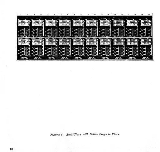
Amplifiers with Bottle Plugs in Place •••••••••••••••••• 10
Installation of Patch Blocks in Pre-Patch Panel •••••••. 12
Dual DC Amplifier, Model 6.712 ... . 14
Model 6.712, Patched as an Inverter •••••••..•••..•••••. 16
One Channel of Dual DC Amplifier, Model 6.712,
Simplified Block Diagram... 19
One Channel of the Model 6.712, Simplified Schematic •••
Frequency Response Test Circuit
. ... .
Test Circuit for Measuring Amplifier Offset ••••••••••••Test Circuit fpr Measuring Noise •••••••••••••••• ~ ••••••
Output Current Test Circuit ••••••••••••••••••••••••••••
Amplifier Troubleshooting Guide
.
... .
Stabilizer Section Test Circuit and Test Points ••••••••Symptoms and Possible. Causes of Amplifier Malfunc.tions •
Dual Integrator Network, Model 12.1116 •••••••••••••••••
Patching an Amplifier to an Integrator, Showing Simpli-fied Schematic of an Integrator Network •••••••••••••
Block Diagram and Symbol for an Integrator
.
... .
Figure Number
20.
21.
22.
23.
24.
25.
26.
27.
28.
29.
30.
31.
32.
33.
33a.
34.
35.
36.
37.
38.
39.
40.
ILLUSTRATIONS .(Cont)
Title
Operational Check Circuit ••••••••••••••••••••••••••••• 36
Initial Condition Resistor Ratio Check Circuit •••••••• 36
Integrator Drift Rate Check Circuit ••••••••••••••••••• 36
Symptoms and Probable Causes of Some Integrator
Mal-func tions ...•... 0 • • • • • • • • • • • • • • • • • • • • • • • • • • • • • • • • • • 38
Quarter-Square Multiplier Patching •••••••••••••••••.••
40
Quarter-Square Multiplier, Simplified Schematic ••••.•• 42
Error Tes t .••.•.• 0 • • • • 0 • • 0 • • • • • • • • • • • D 0 0 • • • • • ~ • • • • • • • •
44
-Quarter-Square Multiplier Adjustment •••••••••••••••••• 46
X2 DFG Pa tching ••••••••••••••••••••••••••••••••••••••• 48
X2 DFG, Simplified Schematic •••••••••••••••••••••••••• 50
X2 DFG Adjustment Information •••••••••••••••••••••••••
51
Log X and 1/2. Log X DFG Patching •••••••••••••••••••••• 54
+Input Log X DFG, Simplified Diagram •••••••••••••••••• 56
Adjustment Information Log X DFG's ••••••••••••••••••••
57
VDFG Mounting Locations ••••••••••••••••••••••••••••••• 60
+VDFG Pa tching and Symbo 1 ••••••••••• '.' •••••••••••••••• 63
+Fixed Breakpoint VDFG Unit, Simplified Schematic ••••• 64
+Variab1e Breakpoint VDFG Unit, Simplified Schematic •• 66
VDFG Test Circuit •• o • • • • • • • e • • • • • • • • • • • • • • e " • • • • • • o • • • 68
Attenuator Schematic •• o • • • • • • o • • • • • • o • • • • • • • • • o . o • • • • • 70
Schematics and Symbols for Attenuators ... . 70
Figure Number 41. 42. 43. 44. 45. 46. 47.
48.
49. 50. 51. 52. 53. 54. 55. 56. 57. 58. 59. 60. 61.62.
63.
64.ILLUSTRATIONS (Cont)
Title
Circuit for Setting Voltage Switching Level
. ....
Sensitivity and Switching Time Test Circuit
.
....
Test Waveform •••••••••••••••••••••••••••••••••••Model 40.538 Electronic Comparator ••••••••••••••
Comparator Unit, Functional Block Diagram •••••••
Electronic Switch Unit, Functional Block Diagram
Comparator, Simplified Schematic ••••••••••••••••
Electronic Switch, Simplified Schematic •••••••••
Gate Output Offset Test Patching ••••••••••••••••
Gate Junction Offset Test Patching ••••••••••••••
Control Area of the TR-20
.
... .
Readout Circuits, Simplified Schematics
...
Relay Bus Driver, Simplified Schematics . ,..
...
Patching an Amplifier to a Rep-Op Integrator Showing Simplified Schematic of Integrator
Network •••••••••• e.e • • • • • • • • • • • • • • • • • • • • • • • • • • • •
Reset and Operate Time Adjustment •••••••••••••••
Improper Waveforms ••••••••••••••••••••••••••••••
Locating an Integrator with an Average Start Time
Start Time Error Test ••••••••••••••••••••••••••••
Simplified Diagram of Wiring for Display Networks
Overload Indicator, Simplified Schematic
...
Overload Indicators, Simplified Wiring Diagram ••
Power and Reference Supplies ••••••••••••••••••••
Reference Regulator, Model 43.037, Simplified
Schetnatic ••••••••••••••••••••••••••••••••••••••
Reference Balance Test Circuit ••••••••••••••••••
INTRontx:TION·
TR-20 MAINTENANCE MANUAL
An Operator's Reference Handbook and a Maintenance Manual are provided with each
TR-20.
The Operator's Reference Handbook provides programming procedures, andsufficient information on computer operation to enable the user to interconnect computing components and to operate the computer without difficulty. ThiS publica-tion is the maintenance manual for the
TR-20
and its contents have been arranged in accordance with that use. The manual is divided into sections that describe a particular computing component or a group of related circuits. A technically qualified person will find the circuit desoriptions an adequate guide in under-standing the operation of the equipment. Persons who are not familiar with analog devices are referred to AppendiK I for a discussion of some elementary principles.INTEGRATOR NETWORKS AND NON-LINEAR
COMPONENTS
AMPLIFIER SELECTOR SWITCH
NULL POT AND REF -SELECTOR SWITCH
MODE CONTROL SWITCH
VOLTMETER FUNCTION
SWITCH
-COEFFICIENT ATTENUATORS
PRE-PATCH
iI~ PANEL
~ .•
",1
. r
~RE-PATCH
PANEL LOCKING LEVERVOLTMETER
COMPUTE TIME SWITCH
ION SWITCHES
REPETITIVE OPERATION CONTROL PANEL
[image:15.623.83.553.62.744.2]VOLTMETER RANGE SWITCH
Figure la. Typical TR-20 Computer, Front View
DC BUS
#2 {
+REF -REF
HQ GND
POWER BUS BYPASS _ _ _
NETWORK, NWI
POWER
SUPPLY----REFERENCE AMPLIFIERS
~f---- CR I AND CR2
{
-15V DC
DC BUS +15V DC
#1 +30VDC
±GND HQ GND
RELAY BUS DRIVER
DISPLAY CONNECTOR
SLAVE CONNECTOR
J37
AC POWER CONNECTOR (AC)
TIMING UNIT FOR EPETITIVE OPERATION
CHAPTER I
THE TR-20 COMPUTER
1. GENERAL DESCRIPTION
The
PAC~
TR-20, Figure 1, is a general purpose analog computer designed and manu-factured by Electronic Associates, Inc. Composed of solid-state computing components, the TR-20 is compact in size, has low power requirements, and does not need special cooling equipment in order to operate in normal office or classroom environments. A fully expanded computer consumes less than 60 watts.The computing components (see Figure 2) in the TR-20 occupy cradles above the slant-ing control panel area. The cradle area is divided into three rows, the top row contains the coefficient attenuators; the middle row house~ the integrator networks, comparators and other non-linear computing components; the bottom row provides space for twenty (10 dual units) operational amplifiers.
The computing components are constructed on plug-in chassis. The front of each com-puting component consists of a color-coded plastic patching block that contains the input and output terminations for the unit. The computing components are inter-connected by placing patch cords between the appropriate input and output termina-tions. TR-20 Computers may be equipped with a removable pre-patch panel that allows problem patching away from the computer. The pre-patch panel consists of a rigid aluminum frame with individual rows that contain patching blocks identical to the patching blocks that form the front panels of the components. Contact between the pre-patch panel and the computing components is accomplished by means of gold plated contact springs.
4.
EQUIPMENT COMPLEMENTThe components contained in and available for the TR-20 Computer are listed in Table 1.
The TR-20 Computer cabinet accepts the plug-in computing. components listed in Table I in five areas as follows:
~. Attenuator Row
This is the top row of computing components. It is wired to accept a maximum of 10 dual coefficient setting potentiometer plug- in modules (20 potentiomete·rs).
~. Non-Linear Row
(a) 12.1116 Integrator Network
(b) 6. 712 Dual DC Ampl(fier
[image:17.612.38.563.65.749.2](c) 16.306 Variable Diode Function Generator
£.
Amplifier RowThis is the bottom row of computing components. It is wired to accept a maximum
of 10 dual amplifier modules (20 amplifiers).
d. Control Panel Area
This is the area on the right side of Control Panel 20.734. Three positions are
available (numbered left to right) to accept the following accessory equipment:
(1) Position CPl. High Speed Repetitive Operation Control Panel, 20.532.
(2) Position CP2. Type 20.366 Function Switch Assembly.
(3) Position CP3. Type 42.185 Quad Coefficient Setting Potentiometer Panel.
e. The VDFG Area
This area is located behind the hinged cover below the control panel. Space is
pro-vided for housing up to six VDFG units in slide-out tray~ The slide-out feature
makes the adjustment pots readily accessible for function setup.
Certain TR-20ls, such as those that are equipped with a Reactor Kinetics Network.
or a Transport Delay Simulator, will have different arrangements.
Non-Linear computing components (multiplier; DFG1s, etc.) are housed in full-width
(1-1/2 inc~~s) or half-width (3/4 inches), plug-in modules that are interchangeable
in the no~-linear row. This row consists of twenty 3/4-inch positions numbered to
correspond to the numbering strip across the top of the row. It has the capacity
for mounting twenty half-width modules, or ten full-width modules, or any
combina-tion of both which does not exceed the total capacity of the row. Full-width
modules occupy adjacent odd and even numbered position pairs, i.e., 1 and 2, 5 and 6, etc.
The non-linear row makes provisions for the following inter-changeable components in any combination (within the limitations described below), providing that the total capacity of the row is not exceeded.
(1) Integrator Networks. Up to nine Type 12.1116 or Type 12.1115 Dual
Networks can be accommodated in positions 1 through 18. Each dual network occupies adjacent position pairs.
(2) Multipliers. Up to nine Type 7.045 Quarter-Square Multipliers or 7.117
TABLE 1. TR .. 20 COMPONENTS
"
GROUP COMPONENT
COMPUTING COMPONENTS
1 Dual DC Amplifier
2a Dual Integrator Network (Non-Rep-Op)
2b Dual Repetitive Operation Integrator Network
3a Quarter-Square Multiplier
3b Bi-Polar Quarter-Square Multiplier
4a X2 Diode Function Generator
4b Log X Diode Function Generator
4c 1/2 Log X Diode Function Generator
4d Sine/Cosine Diode Function Generator
5a Variable Diode Function Generator Group
Consists of:
-Variable Diode Function Generator
+Variable Diode Function Generator
+VDFG Readout Module
5b Variable Diode Functipn Generator Group
Consists of:
+Variable Diode Function Generator
-Variable Diode Function Generator
VDFG Readout Module
5c Variable Diode Function Generator Group
Consists of:
±Variab1e Diode Function Generator
VDFG Readout Module
MODEL I
NUMBER
6.712
12.1116
12.1115
7.045
7.117*
16.101
16.126
16.133
16.313*
2.713-0
16.154-1
16.156-1
16.310
2.645
16.304 -1
16.306 -1
16.308
2.752
16.165-1
[image:19.618.59.577.39.748.2]'GROUP,· 6a 6b 6c 6d 7a 7b 7c 8a 8b 9 10 11 12 COMPONENT
COMPtrrING COMPONENTS (Cont)
Attenuator Group
Attenuator Group
Attenuator Group
Attenuator Group
Consists of:
Attenuator Panel
Readout Module
Referehce Network
Tiepoint Network
Dual Function Switch Group
Consists of:
Function Switch Assembly
Readout Module
Signal Comparator
Electronic Comparator
Regulated Power Supply
Reference Regulator
Dual DC Amplifier
OPTIONAL COMPONENTS AND ACCESSORY EQUIPMENT
Repetitive Operation Expansion Group
Consists Of:
High Speed Repetitive Operation Control Panel
Repetiti~eQperation Timing Unit
MODEL
GROUP COMPONENT .".
NUMBER"
OPTIONAL COMPONENTS AND ACCESSORY EQUIPMENT <Cont)
Dual Repetitive Operation Integrator Network 12.1115
13 Display Unit** 12.987
14 Reactor Kinetics Group 2.475*
15 Transport Delay Simulator 2.448*
16 Audio Overload Alarm 13.017
17 Slave Cable 510.038
18 Patching Kit 100.007
-
51.03919 Se,rvice Shelf
20 AC Power Cable 51.040
21 Pre-Patch Panel 5.235
22 Rep-Op Slave Panel 20.567
AUXILIARY EQUIPMENT
1
VARIPLOTTE~
11102 Repetitive Operation.Display Unit 34.035*
(3) Variable DFG. The available models of the variable DFG can be accommodated in any even numbered position with the exception of position 20.
, .
(4) Fixed Diode Function Generators (Half Width). The TYpe 16.101 X2 Function Generator. the Model 16.126 Log X Diode Function Generator, and the Model 16.133 1/2 Log X DFG are housed in half-width modules, and may be placed in any even numbered position with the exception of pOSition 20.
*These Components described in separate manuals.
(5) Fixed Diode Function Generators (Full Width). The Model 16.313 Sinel Cosine Diode Function Generator is housed in a full-width module, and may be located
in adjacent position pair 17-18 only.
(6) Reference Panel. The Type 12.266 Reference Panel can be positioned in
any even numbered position with the exception of position 20.
(7) Dual Tie Point Panel. Thi5 unit can be used in any position in the
non-linear row.
(8) Comparators. The Type 6.143 Relay Comparator may be used in position
18 only. The Type 40.538 Electronic Comparator may be used in adjacent position
pair 17-18 only.
(9) Function Switch Patching Module. The Type 12.264 Patching Module may
be mounted in position 19 only.
(10) Quad Potentiometer Patching Module. The Type 12.265 Patching Module
may be mounted in position 20 only.
(11) Displa.y Module. This module is required onLy i f the electronic
comparator is ~ supplied. It can be placed in position 17 only.
NOTE
The above assignment of computing components applies to the standard TR-20 Computers. Special computers may be supplied with pro-visions for mounting DFG's or reference panels in the odd numbered positions (with the
exception of position 1) or for accommodating more than one.comparator.
3. OPERATING AND MAINTENANCE ACCESSORIES
In addition to the components listed in the preceding paragraph, each TR-20
in-cludes a group of operating and maintenance accessories. These items are listed
in Table I.
4. PRELIMINARY CHECKOUT
Each TR-20 is completely tested prior to shipment and should be ready for
opera-tion upon receipt. However, asa matter of good practice, it is recommended that
the procedures below be followed as a preliminary checkout.
a. Visual Inspection
Make a visual inspection of the computer. Look for signs for shipping damage.
Become familiar with the location of all components (refer to Figure 1). Check
pre-patch panel are positioned in the same order as the computing components. The switches in the control area should be positioned as follows:
Power ON-OFF Switch
...
OFFMode Control Switch
...
RESETVoltmeter Function Switch •••••••• VM
Voltmeter Range Switch •••••••••• OFF
COMPUTE TIME MILLISEC Switch ••••• OFF
b. Insertion of Pre-Patch Panel
As shown in Figure 3, hold the pre-patch panel at a slight ~ngle and place it in
the patch bay groove. Move the pre-patch panel to the right until it contacts
the right-hand side of the patch bay. Gently push,the pre-patch panel forward
until it is flush with the computer. Turn the locking lever down (the pre-patch
panel will slide to the left).
Co Feedback for the Amplifiers
All operational amplifters should be provided with feedback whenever the computer
~turned on. Connect bottle plugs or patch cords as shown in Figure 4.
do Application of Primary Power
The TR-20 is designed to operate from a 50 to 60 cycle ac supply. The ac circuits
are factory-wired for 110 vac or 220 vac as specified in the purchase order for
the computer. (Drawings DOlO 179 OS and DOlO 179 OW show the required changes
for converting from one power level to the other.) A three wire power cable is
furnished for connecting primary power to the TR-20. The power cable is terminated
in a parallel ground (3-prong. polarized) plug for connection to a parallel ground
receptacle. If the primary power line to which the computer is to be connected
is not equipped with such a receptacle, a parallel ground adapte·r (adapts 3 prong
appliance plugs for use in standard 2 prong outlets) must be used. In this case,
two precautions should be observed:
(1) The power cable should be connected so that the ground side of the
ac line is connected to the ac common line of the computer. The ac common line
is terminated on pin 1 of the ac power connector; see Drawings D045 078 OW, Sheet 2 and B045 078 OW, Sheet 3.
(2) The ground wire on the adapter must be connected to earth ground.
e. Operational Check
Place the., power ON-OFF switch in the ON position. The amplifier overload indicators will flicker briefly, then go out. If an overload indicator remains on, try to balance the amplifier (see Chapter 11).
Next, measure the power supply output voltages and adjust them i f necessary. Balance the amplifiers and verify that they will perform as inverters. (Place one end of a patch cord into a minus reference voltage termination; connect the other end to a I input of each amplifier. Connect a voltmeter to the 0 termination of the ampli-fier; the output should measure +10 vdc.)
Check out all other computing components in turn by applying selected inputs and observing the proper output. The sections of the manual that describe the patch-ing for a component are helpful here since they show typical patchpatch-ing schemes. If any difficulties arise, reference to the appropriate section of this manual should help to clear them up.
5. INSTALLATION OF PATCHING BLOCKS AND CONTACT SPRINGS
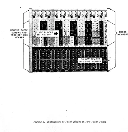
The patching blocks in the pre-patch panel are installed or changed by proceeding as .follows:
~. Lay the pre-patch panel on a flat surface. Remove the four hex head screws from the left .side. (See Figure 5.)
£.
Remove the left side member by sliding it off the four mounting pins. The mounting pins will remain in the cross members when the side member is removed.c. Slide the blocks out of the row. Position the blocks in the desired order •
.!!.
Replace the left side member. Take care to fit i t .properly over the mounting pins. Tighten the four side screws quickly. Be sure that the patching blockson the pre-patch panel are pOSitioned in the same order as the computing components.
The contact springs can be inserted and removed with a pair of long-nose pliers. The patching blocks on the computing components have small orientation holes near each banana receptacle. The projection on the contact spring goes into this hole and the spring is held at tne proper angle. Do not install more than one spring for each group of input or output terminations. That is, for the amplifier (as an example), only one spring is required for the 0 terminations.
6. CHASSIS AND ETCHED CARD REMOVAL
The computing components of the TR-20 are packaged as plug-in components so that installation and removal can be accomplished easily.
A
U-shaped metal chaSSiS provides mechanical strength and affords shielding between the component andREMOVE THESE SCREWS AND TAKE OFF SIDE
[image:27.634.57.548.241.743.2]MEMBER
Figure 5. Installation of Patch Blocks in Pre-Patch Panel
studs on the rear of the chassis. The etched-circuit card is positioned in the metal housing by guide slots and held in place by screws that pass through tapped blocks.
The computing components are removed as follows:
~. At the rear of the TR-20, use a 3/16 inch Spintite to remove one of the hex nuts.
£.
Loosen the second nut approximately 3/8 inches.c. Strike the back of the wrench with the palm of the hand to break the mated connectors apart.
~. Remove the second nut and pull the component from the shelf.
The etched-circuit cards are removed from the metal chassis as follows:
a. Remove the two screws at the rear of the card.
£.
Flex the metal chassis and slide the rear of the card loose.c. To remove the front plastic block, flex the metal chassis and slip the block from its locKing tabs.
7. OUTPUT DEVICES
Digital voltmeters, XY plotting boards, strip chart recorders, and oscilloscopes are in general use as output devices for the TR-20. EAI's 5000 and 5001 TDVM's are high quality, transistorized digital voltmeters that can be used to measure dc potentials in the computer. The EAI Model 1110 VARIPLOTTER, equipped with a
CHAPTER II
DUAL DC AMPLIFIER, M:)DEL 6.712
1. INTRODUCTION
The Dual DC Amplifier, Model 6.712, Figure 6, consists of two independent high-gain amplifiers packaged in a plug-in module together with two independent pre-cision resistor networks. Each amplifier may be used in conjunction with appro-priate networks to perform linear computations such as summation, integration,
and multiplication by a constant. Accessory components enable the amplifier to
be used for operations such as multiplication and division of variables, and the generation of analytic or arbitrary functions,
2, TECHNICAL DATA
Output Voltage Range •.•••••...••.••.... , •...• o. ±lOV, Minimum
Offset (At the Summing Junction)
Unity-Gain Inverter with 10K Resistors 20 jJ..V, Maximum
10 jJ..V, Typical
Output Current at ±10 VDC •.••.••...••. 0 • • " • • ±20 MA, Minimum
(Drives 500 Ohms)
Frequency Response (3 db Down), for a Unity-Gain Inverter with 10K Resistors
20 MI, P-P Input 200 KC, Minimum
300 KC, Typical
Noise (Peak-to-Peak) from DC to 500 KC ... , 200 jJ..V, Maximum lCO jJ..V, Typical
3, OPERATING CONSIDERATIONS
.§j., Patching
The input (B) and output (0) of each amplifier are terminated on the patching
block, together with one end of each of the five input/feedback resistors, The
other end of each resistor is connected to a common bus terminated at the
sum-ming junction (SJ) terminal. To patch an amplifier as a standard inverter or
summer, connect a four-prong bottle plug as shown in Figure 7. A single input applied to a 1 terminal (for example, +X) is inverted and appears as -X at any
of the 0 terminals. If two inputs (for example +Y and +Z) are applied to 1
-Ein
INVERTED OUTPUT
AVAI LABlE HERE
The operational amplifiers are rated for a maximum output of :1::10 volts. The amplifier patching arrangement should be such that the output voltage does not
exceed this limit. (The amplifiers are capable of producing outputs up to :1::13
volts, depending on load, in order to ailow for minor scaling discrepancies.)
It is important to note that all amplifiers m~st be provided with feedback
even if they are not being used in a problem. This is most easily accomplished
by inserting a four-prong bottle plug as shown in Figure 7. When the amplifier is
usedinconjunction with an integrator netwo=k or one of the non-linear components, its patching requirements are discussed in the chapter pertaining to these units.
E.
Amplifier BalancingUnder normal Circumstances, the amplifier will remain balanced for periods of
weeks. HOyTever, at intervals it is desirable to check this condition, and if
an amplifier is found to be unbalanced,then an adjustment should be made. The period between balance checks depends to a large extent on the application
of the amplifier. For uses which might be unusually sensitive to amplifier
un-balance or integrator drift, the amplifier should be un-balanced at more frequent
intervals. In any case, maintenance personnel sho~ld recognize the fact that
most amplifier and network malfunctions Can be detected by checking amplifier balance. Consequently, it is recommer.ded that a check o£ amplifier balance be
made once a week. If the check indicates that the amplifier balance is within
two or three divisions of zero (on the voltmeter), no adjustment need be made.
The amplifier must have some sort of feedback in order to be balanced. Normal-ly this reqUirement is satisfied by the circuit in which the amplifier is
con-nected. The amplifier may be balanced while normal inputs are applied. Each
amplifier has a balance potentiometer that is located behi~d a hinged cover
plate below the control panel. The balance potentiometers are labeled with the number of the amplifier they serve. To balance an amplifier, proceed as follows:
(1) Place the computer ·in the ~!; mode. Place the voltmeter
func-tion switch in the BAL posifunc-tion. Rotate the AMPL SEL switch to the number of the amplifier to be balanced.
(2) Vary the appropriate amplifier belance control until the
volt-meter reads within two or three divisions of zero. (The amplifier over load
indicator may be triggered during the balancing process,)
When the computer is first turned on, a check of amplifier balance may show meter deflections that are slightly high, but they will return to their normal
levels after a warm-up period. For unusual problems that might be sensitive
s.
OverloadsThe computer is equipped with an overload alarm system that indicates the presence
of an overloaded amplifier. The visual overload alarm is located to the left of
the control panel. The lamps are illuminated whenever their associated amplifier
is overloaded. The computer may also be equipped with an audio overload alarm unit
lo~ated :in the rear of the 'IR-20; this unit provides an audible alarm whenever any
ampLifier is overloaded.
l~. CIRCUIT DESCRIPTION
The elementary principles of the operational amplifier are diecussed in Appendix I.
~. B~sic Block Diagram
Each chann~ of the Model 6.712 Dual DC Amplifier consists of a dc amplifier
sec-tion, a chopper (Dl), and a stabilizer amplifier connected as shown in Figure 8. (The dashed components are external to the amplifier chassis.) The circuit is arranged in such a manner that the drift-free characteristics of an ac amplifier and the high frequency response of a dc amplifier are both realized. The re-sulting circuit also has an extremely high gain at low frequencies.
Inputs to the amplifier are applied through the input impedance Zin' The dc and
low frequency components of the signal voltage at the summing junction (SJ)
can-not pass directly to the input of the dc amplifier section because of Cl.
In-stead9 they a~e connected through R14 to contact 3 of chopper Dl. (A chopper or
synchtonous vibrator consists of a coil-driven vibrating reed (2) that alter-. nates between the contacts (1, 3) on each half cycle of the coil excitation
volt-age.) The chopper alternately grounds contact 3 producing.a 60 cps square wave input to the stabilizer amplifier. After amplification, the reSUlting signal is de-modulated (or synchronously rectified) at the second contact (1) of the
chop-per. The reSUlting signal at contact 1 is pulsating dc whose polarity is the
same as the polarity of the signal at the summing junction. The dc Signal is filtered by Rl5 and C2 and applied through Rll to the input to the dc amplifier section. Thus dc or very low frequency signals are amplified by the stabilizer amplifier and by the dc amplifier.
The circuit from contact 3 of Dl to contact 1 is a modulated carrier-type ampli-fier that provides high gain de amplification with very low drift. The
stabi-lizer is phase sensitive; if the polarity of the summing junction signal changes, the phase of the modulated signal changes and the polarity of the pulsating dc output voltage changes.
High freq~ency components of the input Signal are passed by Cl to the dc
ampli-fier, and are amplified by the gain of the dc amplifier only. The open loop gain of the amplifier thus depends on the frequency of the input signal. At very low frequencies, the gain is extremely high because the stabilizer
ampli-fier is placed in cascade with the dc ampliampli-fier. At higher frequencies, the
r--,
r---
I Ift---j
I L __ .J I
I CI I
1 RIO I
I I
I I
I I
1 I
.1 I
r---,
RI4 RI5E hi'" - ; Z in I- 1--~_'VV\r~~_'VI./'Ir+___l Eo
L ___ J SJ
1
I
1
r---...,
L_-, OVERLOAD I
L'~~~~~~
r--- -ISV
I c"" BAL
'---< ... POT
I
-One of the criteria for a high quality operational amplifier is that the output voltage be zero when the input voltage is zero. This zero corresponding
be-tween input and output voltages is called amplifier balance. The manual
adjust-ment process to insure this correspondence is called balancing. As previously described, the balance potentiometer (BAL POT) is adjusted until the amplifier output is zero volts when the input is zero volts. The amplifier would require balancing every few minutes without stabilization. The drift compensation pro-duced by chopper stabilization allows the amplifier to be used for weeks without attention.
Any component of the amplifier output voltage due to drift in the dc amplifier section is fed back through the feedback impedance Zf to the summing junction of the amplifier. Since any drift-produced voltage has a very low frequency, it will be amplified by the stabilizer section, filtered, then applied as a drift-correc-tion Signal to the input of the dc amplifier secdrift-correc-tion. The drift-produced com-ponent in the output voltage is reduced by a factor equal to the effective gain of the stabilizer section.
The amplifier in the stabilizer section has a gain of about 1000. Since it is
connected to the summing junction, it serves as a monitor of the summing junc-tion voltage. Under normal circumstances, the input current to the operajunc-tional amplifier is equal to the feedback current, and the summing junction is at
vir-t~al ground. If the currents are not equal, the amplifier is not performing
properly, and the summing junction departs from virtual ground. This rise in voltage is amplified by the stabilizer and results in a large output signal that
is used to trigger an overload indicator which informs the user that the ampli-fier is not operating properly. Because the stabilizer is a sensitive monitor of the summing junction voltage, the magnitude of its output voltage is an in-dication of the balance of the amplifier. The amplifier is balanced accurately by connecting the stabilizer output to the voltmeter on the control panel and adjusting the balance potentiometer until the voltmeter reads zero. Note that it is not necessary to remove the inputs to the operational amplifier during the balancing process since all circuit requirements are satisfied if the sum-ming junction is at virtual ground. A feedback resistor must be connected around the amplifier before the balancing procedure can be accomplished.
The schematic diagram of the dual amplifier used in the TR-20 is shown on
Draw-ing D006 282 OS in the rear of this manual. Each amplifier consists of a
six-transistor dc amplifier and a three-six-transistor stabilizer amplifier. Each
amplifier uses a set of contacts of chopper Dl. The coil excitation voltage
(6.3 vac, 60 cps) for Dl is obtained from Regulated Power Supply, Model 10.179,
which also provides the other operating voltages for the amplifier. Since each
of the dual amplifiers is identical, the following circuit description is con-fined to the amplifier shown in the upper half of the schematic. A simplified schematic to be used with the following description is shown in Figure 9.