HEWLETT-
PAC.KARD
+
•
~
Technical
Reference
Manual
•
•
•
Portable PLUS
Technical
Reference Manual
...- - - -"
---:---:---...,.-:---Notice
Hewlett-Packard makes no warranty of any kind with regard to this material, ~
including, but not limited to, the implied warranty of merchantability and fitness for a " J particular purpose. Hewlett-Packard shall not be liable for errors contained herein or
for incidental or consequential damages in connection with the furnishing) performance) or use of this material.
Hewlett-Packard assumes no responsibility for the use or reliability of its software on equipment that is not furnished by Hewlett-Packard.
(c)Copyright 1985) Hewlett-Packard Company.
This document contains proprietary information) which is protected by copyright. All rights are reserved. No part of this document may be photocopied) reproduced) or translated to another language without the prior written consent of Hewlett-Packard Company. The information contained in this document is subject to change without notice.
Restricted Rights Legend. Use) duplication) or disclosure by the Government is
~
subject to restrictions as set forth in paragraph(b)(3)(B) of the Rights in TechnicalData and Software clause in DAR 7-104. 9(a).
MS1Mis a U.S. trademark of Microsoft Corporation.
1M TM .
1- 2- 3 and Lotus are U.S. trademarks of Lotus Development CorporatIon.
Portable Computer Division 1000 N.E.Circle Blvd. Corvallis, OR 97330, U.S.A.
Contents
Chapter Page
1 Overview
1.1 About This Manual 0 0 0 • • • • 0 • • • • • 0 • • 0 • • • • • • • 0 0 • •0 0 0 • • • • • 0 0 1-1
1.2 Options for Accessing the System .. 0 • • • • • • • • • • • • • • • • 0 • • • • • • • 1-2
1.2.1 Accessing the Display 0 • • • • • • • • 0 1- 2
1.2.2 Accessing Communications Devices ..0 0 • 0 • • • • • • • • • • • 0 • 0 • 0 • • 1-3
1.3 References .0 • • • • • • • • • • •0 • 0 0 • • 0 0 0 • •0 • 0 • 0 0 0 0 • • 0 • 0 0 0 • • 0 0 0 1-4
2 2.1 2.2 2.3 2.3.1 2.3.2 2.4 2.4.r 2.4.2 2.4.3 2.4.4 2.4.5 2.4.6 2.4.7 2.4.8 2.5 2.6 2.7 2.8 2.9 2.1 0 2.10.1 2.10.2 Electrical Design
Introduction 0 • • • • • • •0 • • • • • • 0 • •0 • 0 • 0 0 • • • • • 0 0 • • • • • • 0 • • 2-1
Memory Map o. 2- 3
Operating Modes 0 0 • • • • • • • • • • • • • • • • • • • 2-4
Sleep Mode 0 • 0 • •0 • • • 0 • • • • • • 0 0 • 0 • • • • • 0 • • • • • • • • • • • • • 2-5
Stop Mode 0 • • • • • • 0 0 . 0 • • 0 0 • 0 • 0 • • • 0 0 0 0 0 0 • 0 0 0 0 0 0 0 0 0 o. 2-7
Mainframe Hardware .o • • 0 0 0 . 0 0 0 0 . 0 • • 0 0 • • 0 0 0 0 0 o ' 0 0 0 0 . 0 • • • 2-7
CPU ... 0 o '0 0 ' 0 0 • • • • • • • • • • 0 • • • • • • • • • • • • • • • • • • 0 0 0 . 0 2-9
Clocking .0 • 0 • • 0 • • • • • • • • • • • • • • • • • • 0 • • • • • 0 • • • • 0 0 0 • 0 • • • 2-9
Ready Circuit .... 0 • • • • • • • • • • • • • 0 • 0 • • •0 • • • • • • • • • • • • • 0 0 2-9
PPU - Peripheral-Processor Unit ...0 • • • • 0 • 0 0 • • o ' • • • • • 0 0 • • 2-9
Keyboard Interface 0 • • • • •0 • • • 0 • • • • • • • • 0 • • • 0 0 • • • • • • • • • • 2-10
Power Supply 0 0 2-10
Memory Board 0 • • • 0 0 • • • • • • • • • • • • • • • • • 0 0 • • • • • 2 -10
Configuration EPROM 0 • • • • • •0 • • • • • • 0 • • • • • • • • • • • • • 2-10
Serial Interface 0 0 • • • • • • • • • • • • • • 0 • • • • • • • 0 • • 0 0 • • • • • • • 2-13
HP-IL Interface 0 • • • • • • • • 2-19
Recharger Interface
0...
2-19Video Connector 2-23
Modem Connector 0 • • • • • 0 0 0 • • • • • • • • • • 0 . 0 0 . • • • • 2-25
Plug-In Ports . 0• • • • • • • • • • • • • • • • • •0 • • • • • • • • • • 0 0 • • • • • • •0 2-28
Generic Module Description 0 • • • • • • •0 2-28
4 Resetting the Portable PLUS
4.1 Introduction 4-1
4.2 Reset Options 4-2
4.2.1 Reset via (Shlft )(]lID (Break) 4-2
4.2.2 Reset via (Shlft )(]lID (Extend char)( Break) '4-2
4.2.3 Reset via @ 4-2
4.2.4 Reset via the Reset Button . . . .. 4-3
4.3 Re-Boot Screen 4-3
4.3.1 Memory Lost Message 4- 3
4.3.2 Standard Re-Boot Display 4-4
3 3.1 3.2 3.3 3.4 5 5.1 5.2 5.3 5.4 5.5 5.6 5.7 5.8 5.9 5.10 5.11 5.12 5.13 5.14 5.15 5.16 5.17 5.18 5.19 5.20 5.21 Mechanical Design
Introduction 3- 1
Mainframe 3- 2
Modem 3-4
Plug-In Ports 3-6
BIOS Interrupts
Introduction 5- 1
Print Screen Interrupt (Int 5h) 5- 5
Video I/O Interrupt (lnt 10h) 5-5
Equipment Check Interrupt (lnt I1h) 5-12
Memory Interrupt (Int 12h) 5-13
Communications Interrupt (Int 14h) 5-13
Keyboard I/O Interrupt (Int 16h) 5-17
Print Byte Interrupt (Int 17h) 5-19
Reboot Interrupt (Int 19h) 5-20
Time Of Day Interrupt (lnt 1Ah) 5-20
Keyboard Break Interrupt (Int 1Bh) 5-21
Timer Tick Interrupt (Int 1Ch) 5-22
Graphics Character Extensions (Int IFh) 5-23 Modem Transmit Interrupt (Int 40h) 5-24 Modem Ring/Carrier Interrupt (Int 42h) 5-24
Timer 2 Interrupt (Int 43h) 5-24
Plug-in 1 Interrupt (Int 44h) 5-25
Plug-in 2 Interrupt (Int 45h) 5-25
PPU Alarm Interrupt (lnt 46h) 5-25
Death/Battery Cutoff Interrupt (Int 47h) 5-26
Keyboard Interrupt (Int 49h) 5- 27
~.,,,
..,.5.25 5.26 5.27 5.28
-r
5.29 5.30 5.31 5.32 5.33 5.34 5.35 5.36 5.37 5.38 5.39 5.39.1 5.39.2 6 6.1 6.1.1r
6.1.2 6.2 6.3 6.4 6.5 6.6 6.6.1 6.6.2 6.6.3 7 7.1 7.2 7.3 7.3.1 7.3.2~
7.3.3 7.3.4 7.3.5Low Battery Interrupt (Int 4Dh) 5-29
Modem Input Interrupt (Int 4Eh) 5-29
Serial Input Interrupt (Int 4Fh) 5- 30 System Services Interru pt (Int 50h) 5- 31
Modifier Key Interrupt (Int 52h) 5-64
Print Key Interrupt (Int 53h) 5-65
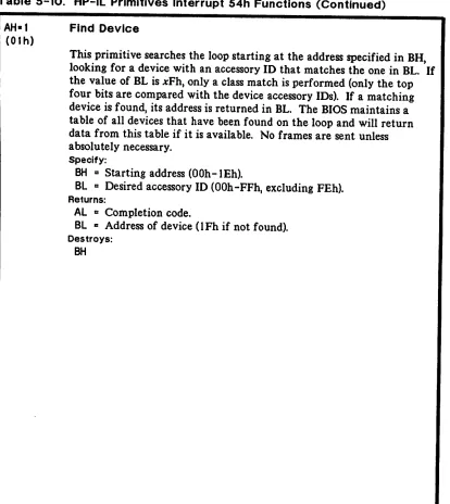
HP-IL Primitives Interrupt (Int 54h) 5-65
Sleep Interrupt (Int 55h) 5-80
Menu Key Interrupt (Int 56h) 5-81
System Key Interrupt (Int 57h) 5-82
Break Key Interrupt (Int 58h) 5-83
Enable/Disable Ring Interrupt (Int 59h) 5-84 AUX Expansion Interrupt (Int SOh) 5-85 CON Expansion Interrupt (Int 5Eh) 5-87
Fast Video Interrupt (Int SFh) 5-94
Fast Alpha 5-94
Fast Graphics 5-113
Built-In Device Drivers
Introduction 6-1
Serial Operation 6- 2
Modem Operation 6-7
AUX, COM1, COM2, COM3, and 82164A Devices 6-9
NUL Device 6-21
CLOCK Device 6-22
LPT1, LPT2, LST, PLT, and PRN Devices 6-22
CONsole Driver 6- 23
CONsole Control Sequences 6-24
Keyboard Operation 6-45
CONsole I/O Control Functions 6-50
Low-Level Hardware Interface
Introduction 7-1
I/O Memory Map 7-1
Multi-Controllers 7-3
Keyboard Interface 7-3
Interval Timer 7-4
Serial Port 7- 5
Multi - Purpose Port 7-7
7.3.8 7.3.9 7.4 7.5 7.5.1 7.5.2 7.5.3 7.5.4 7.5.5 7.5.6 8 8.1 8.2 8.3 8.4
Registers - Interval Timer . . . .. 7-16 Registers - Multi - Purpose Port 7-1 9
HP-IL Controller 7-22
Display Controller 7-26
Display RAM Mapping - Graphics Mode 7-26 ~
Display RAM Mapping - Alpha Mode 7-29 )
Alpha Attribute Bits 7-33
Alpha Cursors 7- 33
Registers 7-34
Softkey Menu Display 7-37
Memory Management
Introduction 8-1
Edisc 8-3
ROM Disc 8-7
Summary of ROM Disc Access 8- 14
9 9.1 9.2 9.3 9.4 9.5 9.6 10 10.1 10.2 10.2.1 10.2.2 10.3 10.3.1 10.3.2 10.3.3 10.4 10.4.1 10.4.2 10.4.3 10.4.4
Plug-In ROM Design
In trod uction .
Plug-In ROM Format .
ROM-Executable Code .
ROM Boot Code .
Constraints on Plug-In ROM Software .
PAM Interface to Plug-In ROMs .
PAM - The Personal Application Manager
Power-Up Sequence .
The PAM Environment .
PAM and AUTOEXEC.BAT Files .
PAM Internal State .
PAM And Application Programs .
Installing Applications in PAM .
The liDOS Commands" Application .
PAM Execution of a Program .
The PAM Configurations .
The System Configuration .
Main Memory and Edisc .
External Disc Drives .
Disc Write Verify .
10.4.8 10.4.9 10.4.10 10.4.11
r
10.4.12 10.4.13. 10.4.14 10.4.15 10.4.16 1004.17 10.5 10.5.1 10.5.2 10.6 10.7 10.8 10.8.1 10.8.2 10.9 11 11.1 11.2 11.2.1 11.2.2 11.2.3 11.2.4 11.2.5 11.2.6 11.2.7 11.2.8 11.2.9 11.2.10 11.3 12 12.1r
12.1.1 12.1.2 12.1.3Cursor Type 10-10
Console Mode 10-10
Tone Dura tion 10- 11
Plotter Interface 10-11
Printer Interface 10-11
Printer Mode 10-11
Printer Pitch, Line Spacing, and Skip Perforation 10-12
Datacom Interface 10-12
The Datacom Configuration 10-12
The Time and Date Configuration . . . .. 10-15
PAM And Alarms 10-16
The PAM.ALM File . . . .. 10-16
When an Alarm Occurs 10-16
Autoanswering: PAM and Ring Interrupts 10-17
The Battery Fuel Gauge 10-18
PAM Help Facility 10-19
Installing PAMHELP.COM 10-19
After PAMHELP.COM Is Installed 10-19
Bypassing PAM With COMMAND.COM 10-21
Boot Sequence Options
Introduction 11-1
Boot Sequence 11-2
Built -In Diagnostics 11-2
Recover From Sleep . . . .. 11-2 ROM Slot 7 Boot Code Before Changing RAM 11-2 Config EPROM Boot Code Before Changing RAM 11-3 ROM Slot 7 Boot Code After Some Initialization 11-3 Boot Code From the Config EPROM After Initialization 11-4 Boot Using the CONFIG.SYS on the ROM in ROM Slot 7 11-4 Boot Using the CONFIG.SYS on the Default Drive 11-4 PAM Executes AUTOEXEC.BAT From ROM Slot 7 11-5 PAM Executes AUTOEXEC.BAT From Drive A: 11-5 The CONFIG.SYS File . . . .. 11-5
Modem Interface
Overview 12-1
Command Mode and Data Mode 12-1
Commands 12-2
12.1.6 12.2 12.3 12.4 12.5 12.6 12.7 12.7.1 12.7.2 12.7.3 12.7.4 12.7.5 12.8 13 A A.1 A.2 A.3 A.3.1 A.3.2 A.3.3 A.3.4 A.3.5 A.3.6 A.3.7 A.3.8 A.3.9 A.3.1 0 B C D E
Default State of the Modem 12-5
Modem Commands 12-6
Dialing 12-12
Modem Responses . 0 • 0 • • • • • • • • • 0 0 0 0 0 • • • 0 0 • • 0 • 0 0 0 • • • • 0
o.
12 -1 3S-Register Description 0 • 0 • • • 0 • 0 • • 0 • • • • • • • • • • • • • • • • • 12-15
Hayes Compatibility 0 • • • • • • • • • • • • • • • • • • • • • • • • • • • • 12-20
Special Considerations for Programmatic Control
.0
0...
12-22Modem Power-On Problem 0 12- 22
Ignores Characters While Responding 0 0 • • • • • • • • • • • 12-22
Can't Dial Out While Receiving Ring . 0 • • • • 0 • 0 • • • 0 0 0 0 • • • 0 12-23
Spurious Extra Characters Generated 0 • • • • 0 • 0 • 0 • • • 0 • 0 • • 0 0 12-23
Spurious Interrupts at Power-Up 0 0 . 0 . 0 • 0 • • • • •0 . 0 0 .• • • • • 12-23
Directly Connecting Two Modems .. 0 • 0 0 • • • • • • • • • •0 0 • • 0 • • • 12- 23
Keyboards and Keycodes
Comparisons With Other Computers
Comparison With the HP 110 o. 0 • • • 0 0 0 0 • • • • 0 • • • • •0 0 • • • • 0 0 • A-I
Comparison With the HP 150 .0 0 • • • • • 0 0 0 . 0 • 0 0 0 • • • 0 0 0 0 0• • o. A-2
Comparison With the IBM PC 0 • • • • • • • 0 • • • • • • • • • • • • • • • • • •o. A-3
VideoInterrupt(Int 10h) 0 . o. 0 0 . 0 0 • • • • 0 • • • • • • •0 . 0 A-3
Equipment Check Interrupt (Int 11 h) 0 0 • • • • • 0 0 • • • • • 0 0 0 0 • • • A- 5
~
Diskette/Disc Interrupt (Int 13h) 0 • • • • • • 0 0 • • 0 A- 5
Communications Interrupt (lnt 14h) 0 0 • • • • • • • • • • • 0 0 • • • • • • • A-5
Cassette Interrupt (Int ISh) ... 0 • • • • • 0 • • • • • • • • • • • • • • • • • • • A- 6
Keyboard Interrupt (Int 16h) .0 0 • • • • • • • • • • • • • • • • • • • 0 • • • • A-6
Printer Interrupt (Int 17h) 0 • • • • • • • •
o.
A-6Re-Boot Interrupt (Int 19h) .0 • • • • • 0 • • • • • • • • • • • • • • • • • • • 0 A-6
Time-of-Day Interrupt (Int lAh) A-7
Keyboard Break Interrupt (Jnt IBh) 0 . 0 • • 0 • • • • • • •0 • 0 A-7
Schematic Diagrams
Assembler LlsUng for Configuration EPROM Character Sets
F F.I F.l.l F.l.2
r
F.l.3 F.l.4 F.2 F.2.l F.2.2 t G G.l G.2 G.3 G.4 G.5 G.6 G.? G.8r
H H.l H.2 H.3 H.4 J K K.l K.2 K.3 K.3.l K.3.2 K.3.3 K.3.4 K.3.5 Mass StorageDisc Drive Options F-I
Built-In Disc Drives F-l
lIP 9114A HP-IL Disc Drive F-l
HP-IB Disc Drives F-2
Portable PLUS-Desktop Link F-3
Media Compatability F-4
Reading Other Discs on the Portable PLUS F-4 Reading Portable PLUS Discs on Other Computers .. ' F-4
Configuring Serial Printers
Introduction G-l
The HP 2225D ThinkJet Printer G-l
The HP 26QIA Printer G-3
The HP 2686A LaserJet Printer G-5
The IDS-560 Impact Printer - The Paper Tiger G-6
The NEC Spinwriter 3510 G- 8
The Xerox 61 OC 1 Memorywriter G-I0
The Xerox 625C Memorywriter G-12
Portable PLUS-Desktop Link
Portable PLUS to HP 150 H-2
Portable PLUS to IBM PC/XT H-3
Portable PLUS to IBM AT. . . .. H-4 Portable PLUS to Portable (or Portable PLUS) H-4
Parts
Escape Sequence Summary Software Module Configurations
Overview K-1
Plug-In ROMs and EPROMS K-3
Detailed Description K - 5
ROM/EPROM Organiza tion Options K - 5
Jumper and Socket Labeling K-6
Jumpers and Socket Groups K-7
Configuration of the Small Group .. . . .. K-7
Figure
Illustrations
Page
2-1 System Address Space 2- 3
2-2 I/O Address Space 2-4
2-3 Portable PLUS Block Diagram 2-8
2-4 Configuration EPROM Addressing 2-12
2- 5 Serial Connector 2-14
2-6 Modem Cable 2-18
2-7 Printer Cable 2-18
2-8 Automotive Recharger Schematic Diagram 2-22
2-9 Plug-In Connector 2-33
2-10 Plug-In Bus Read Cycle - Lower Memory 2-34
2-11 Plug-In Bus Write Cycle - Lower Memory 2-35 ~
2-12 Plug-In Bus Read Cycle - I/O and Upper Memory 2-36 } 2-13 Plug-In Bus Write Cycle - I/O and Upper Memory 2-37
2-14 Plug-In Bus Interrupt Acknowledge Cycle 2-38
2-15 Plug-In Module Registers 2-43
3-1 Mainframe Dimensions 3-3
3-2 Modem PC Board 3-5
3-3 Plug-In PC Board 3-7
5-1 Interrupt 1Dh Attribute Byte 5-6
5-2 Fast Alpha Structures 5-95
5-3 Display Attribute Byte 5-96
5-4 Initial Font Load 5-97
5-5 Font Formats 5-98
6-1 Serial Interface Timing - Sheet 1 6-4
6-2 Serial Interface Timing - Sheet 2 6-5
6-3 Serial Interface Timing - Sheet 3 6-6
6-4 Keyboard Scancodes 6-48
7-1 I/OAddressSpace 7-2 ,~
8-3 8-4 8-5 8-6 9-1 13-1 13-2 13-3 13-4 13-5 13-6 13-7 13-8 13-9 13-10 13-11 13-12 B-1 B-2 B-3 B-4 B-5 B-6 B-7 B-8 B-9 B-I0 K-l
ROM Disc FAT 8-11
ROM Disc Root Directory 8-12
ROM Disc Fixed Subdirectory Files 8-13 ROM Disc Plug-In File Data . . . .. 8-14
Plug-In ROM Format 9-3
English (U.S.) Keyboard ~ . . . .. 13- 8
English (U.K.) Keyboard 13-11
French Keyboard 13-14
Belgian Keyboard 13-15
German Keyboard 13-18
Italian Keyboard 13-21
Dutch Keyboard 13-24
Swiss (German) Keyboard 13-27
Swiss (French) Keyboard 13-30
Danish Keyboard . . . • . . . 13-33
Norwegian Keyboard 13-36
Swedish Keyboard . . . • . . . 13-39
Motherboard PCA - Sheet 1 B-2
Motherboard PCA - Sheet 2 •... B-4
Motherboard PCA - Sheet 3 ••••••••••••••••••••••••••••••• B-6 Motherboard PCA - Sheet 4 ••••••••••••••••••••••••.•••••• B-7
Memory Board PCA ;0: B-8
Modem PCA B-I0
Software Drawer PCA B-12
Memory Drawer PCA - Sheet 1 B-14
Memory Drawer PCA - Sheet 2 B-16
Memory Drawer Piggy-Back PCA B-18
Table
Tables
Page
1-1 Options for Display Access 1- 2
2-1 Serial Interface 2-14
2-2 Recharger DC Limits 2-20
2- 3 Recharger Series Resistance Limits 2- 21
2-4 Video Signals 2-24
2-5 Video Specifications 2-24
2-6 Modem Connector 2-25
2-7 Specifications for Modem Port 2-27
2-8 Signals for Plug-In Ports . . . • . . . 2-29
2-9 Plug-In Bus Loading 2-39
2-10 Plug-In Power Loads 2-40 /~
2-11 Voltage Levels for Plug-In Bus 2-40 )
2-12 Requirements for Plug-In Drivers 2-41
5-1 Hardware and BIOS Interrupts 5-2
5-2 Video I/O Interrupt 10h Functions 5-7
5-3 Communications Interrupt 14h Functions 5-14 5-4 Keyboard I/O Interrupt 16h Functions 5-17
5-5 Print Byte Interrupt 17h Functions 5-19
5-6 Time Of Day Interrupt I Ah Functions 5-20 5-7 System Services Interrupt 50h Functions 5-31 5-8 System Services Int SOh Detailed Description 5-33
5-9 PPU Commands 5-54
5-10 HP-IL Primitives Interrupt S4h Functions 5-69 5-11 AUX Expansion Interrupt SOh Function 5-86 5-12 CON Expansion Interrupt SEh Functions 5-88 5-13 Fast Video Interrupt SFh Alpha Functions 5-99 5-14 Fast Video Interrupt SFh Graphics Functions 5-114
6-1 AUX I/O Control Commands 6-9 ~
6-6
6-7
6-8
7-1
7-2
7-3
8-1
8-2
9-1
10-1
10-2
12-1
12-2
12-3
13-1
13-2
13-3
13-4
13-5
13-6
13-7
13-8
13-9
13-10
13-11
13-12
13-13
13-14
13-15
13-16
13-17
13-18
13-19
13-20
13-21
13-22
13-23
13-24
13-25
13-26
ANSI Escape Sequences
6-41
CONsole Write I/O Control Functions
6-50
CONsole Read I/O Control Functions
6-51
Multi -Controller Registers . . . • . . .
7-8
UP - IL Registers 7-
22
Display Controller Registers 7- 35
Edisc Sector Oh 8- 5
ROM Disc Sector Oh
8-9
Plug-In ROM Sector Oh
9-4
PAM Internal State
10-
3PAMUELP.COM Parameters
10-20
Modem Commands 1
2-7
Modem Responses 12 -14
Modem S-Registers
12-15
UP Mode Character Codes
13-3
Alternate Mode Character Codes
13-5
Common UP Mode Character Codes • . . . 1
3-6
Common Alternate Mode Character Codes
13-7
English (U.S.) UP Mode Character Codes
13-9
English (U.S.) Alternate Mode Character Codes
13-10
English (U.K.) HP Mode Character Codes
13-12
English (U.K.) Alternate Mode Character Codes
13-13
French/Belgian HP Mode Character Codes 13-16 French/Belgian Alternate Mode Character Codes
13-17
German HP Mode Character Codes
13-19
German Alternate Mode Character Codes
13-20
Italian UP Mode Character Codes
13-22
Italian Alternate Mode Character Codes
13-23
Dutch HP Mode Character Codes 13-25
Dutch Alternate Mode Character Codes
13-26
Swiss (German) UP Mode Character Codes
13-28
Swiss (German) Alternate Mode Character Codes
13-29
Swiss (French) HP Mode Character Codes
13- 31
Swiss (French) Alternate Mode Character Codes 13-32
Danish HP Mode Character Codes 13- 34
Danish Alternate Mode Character Codes . . . .. 13-35 Norwegian UP Mode Character Codes . . . ..
13-37
Norwegian Alternate Mode Character Codes
13-38
Swedish HP Mode Character Codes 13-
40
0-1
0-2 0-3 D-4 G-l
G-2
G-3
G-4
G-5
G-6
1-1 1-2 1-3 J-l J-2 J-3 J-4 J-5
K-l
K-2
K-3
Roman8 Character Set ....•••.•...•.•...•... 0-2
Line-Drawing/Math Character Sets 0-3
Alternate Character Set ...•...•... 0-4
Character Sets - Numeric Listing 0- 5
ThinkJet Switch Settings 0-2
HP 260lA Switch Settings ..•... 0-4
ID5-560 Switch Settings 0-7
5pinwriter 3510 Switch Settings 0-9
61 01 C 1 Memorywriter Option Settings G-IO 625C Memorywriter Option Settings G-13 Portable PLUS Accessories ..•... 1-1
Custom HP Parts 1-3
Standard Parts ...•... 1-3
Control Characters J-l
Two-Character Escape Sequence Summary J- 2 HP Alpha Escape Sequence Summary ...•... J-3 HP Graphics Escape Sequence Summary J- 4
ANSI Escape Sequence Summary J- 5
Wire Jumper Connections for ROMs/EPROMs K- 2
Plug-In ROM Specifications K- 3
ROM/EPROM Organization Options ...•...•... K- 5
r
1
Overview
1. 1 About This Manual
This manual presents information that will help you to develop hardware and software that operate on the Portable PLUS computer. The manual contains information about:
Hardware
• Electrical design.
• Mechanical design.
Software and Firmware:
C ·
Resetting the computer. • BIOS interrupts.• Built -in device drivers.
• Low-level hardware interface.
• Memory.
• Plug-in ROM design.
• PAM (Personal Applications Manager).
• Boot options.
; 1
In addition, appendixes include additional reference information about the Portable PLUS.
Applications designed for the Portable PLUS may be designed to be compatible with
other computers also. (Refer to appendix A for detailed information about .~ compatibility.) The information in this manual will help you maximize compatibility. )
1.2 Options for Accessing the System
The following topics describe various ways you can access certain features of the Portable PLUS. The method you choose will depend upon your particular application. The individual choices are described in different parts of this manual.
1.2.1 Accessing the Display
The Portable PLUS provides six ways to access the display. The methods are listed in table 1-1. They provide the programmer with options for satisfying the specific requirements of a program.
Table 1-t Options for Display Access
Access Method Speed POWf'r Usability Graphics
CON output via Int 21 h 1 3 Simple Full
CON output via Int 50h 2 3 Simple Full
Video I/O Int I Dh 3 2 Moderate Limited
Fast Video Int 4Fh 4 4 Moderate Full
Fast Write via Int 50h 5 1 Simple None
Direct hardware access 6 5 Difficult Primitive
The preferred, most commonly encountered, and most portable method of sending data to the display is CON output via the standard MS-DOS service interrupt, Int 21h. (Refer to "References" below.) Display control can be, accomplished via a fairly
complete set of HP and ANSI escape sequences. A subset of standard HP graphics escape
~:,: .
\
printer hardcopy (via "'P printer on/off toggle») display start/stop control (via "'S/"'Q») and portability to other MS-DOS computers. (Refer to "System Services Interrupt" in chapter S.)
The Video I/O interrupt, Int IOh) provides a subset of the IBM PC Video I/O functions. (Refer to "Video I/O Interrupt" in chapter S.) Its compatability limitations are due mainly to the 480x200 size of the LCD panel and other hardware differences between the Portable PLUS and the IBM PC.
Fast Video (Int 5Fh) functions provide a level of display control similar to Int IOh, but with much more functionality and flexibility. (Refer to "Fast Video Interrupt" in chapter 5.) This set of routines provides very low-level) window-oriented control of display memory in alpha mode, and a relatively full set of graphics manipulation routines in graphics mode.
Int 50h Fast Write is a special service function that can be used to force short messages onto the display without interfering with any other part of the system. (Refer to "System Services Interrupt" in chapter 5.) This is used within the BIOS) for example) to display the "Low Batteryr' warning. Fast Write is a very low-level function that simply forces a specified attribute and string of characters into display RAM with no special processing or safety checks, and should be used only in similar immediate-display situations.
As with most computers) there is the option of "going straight to hardware." Performing your own display control is potentially the fastest) most efficient way of getting the screen to do what you want it to do) although such programming can easily become quite complex) potentially dangerous, and can possibly interfere the normal display operation if mixed with calls to other BIOS-resident display functions--unless you take certain precautions. For the sake of safety and simplicity) applications should refrain from directly accessing system hardware. (Refer to IIDisplay Controller" in chapter 7.)
1.2.2 Accessing Communications Devices
The Portable PLUS can address three communications devices through the system BIOS:
• The serial (RS-232) port.
• A SmartModem-Compatible 1200-BPS modem.
1
Each of these devices is supported by its own device driver, and data can be transferred through them using any of the MS-DOS standard device operations. Various device parameters can be configured through a standard set of IOCTL commands. (Refer to "AUX, COM1, COM2, COM3, and 82164A Devices" in chapter 6.) Also, the MS-DOS AUX device can be "redirected" to address any of the three individual devices.
In addition, the built-in serial port and the modem can be accessed through the IBM PC-compatible software interrupt 14h. (Refer to "Communications Interrupt" in chapter 5.) All IBM PC functions are supported, although some of the status
information returned by this interrupt must be interpreted differently due to hardware incompatibilities. Interrupt 14h gives much better performance than the MS-DOS device calls, but it can be cumbersome to use from high -level languages, and it is not supported on all Hewlett-Packard products.
For applications that must get as close as possible to the hardware, interrupt 5Dh is provided to allow access to each character as it comes into the communications port. (Refer to "AUX Expansion Interrupt" in chapter 5.) This enables a program to achieve the effect of taking over the hardware interrupt, but will not need to duplicate the function of the BIOS.
1.3 References
Although this manual describes the Portable PLUS in detail, you may want to consult additional references for other information. Owner's manuals describe how to operate the system. Other references provide information about standards that are
implemented by the Portable PLUS.
• Hewlett-Packard Company. Using the Portable PLUS.HP part number 45711-90002, (cd985.
• Hewlett-Packard Company.HP 82983A 300/1200 BPS Modem Owner's Manual.
HP part number 82983-90001, (cd985.
• Hewlett-Packard Company.The HP-IL Interface Specification. HP part number 82166-90017, (cd982.
• Kane) Gerry) et aI.The HP-IL System: An Introductory Guide to the Hewlett-Packard Interface Loop.Osborne/McGraw-Hill) Berkeley) California, (el1982.
• Hewlett-Packard Company. HP45419C Programmer)s Tool Kit) which contains:
-Series 100 Programmer's Reference Manual: Microsoft MS-DOS Programmer's Reference Manual.
-Series 100 Macro Assembler Manual: Microsoft Macro Assembler Manual.
1'.. ;: :
r
2
Electrical Design
2.1 Introduction
The Portable PLUS computer features a 25-line liquid-crystal display (LCD), a 76-key full-size (3/4 throw) keyboard, 128K bytes of built-in RAM, 16K bytes of display RAM, 8K bytes of built-in configuration EPROM (expandable to 16K bytes), and 192K bytes of built-in ROM. HP-IL and serial interfaces are built in. A 1200-baud
direct-connect modem and an external video interface are optional.
Listed below are the main specifications for the Portable PLUS. 2
Size:
Weight:
LCD:
Keyboard:
Speaker:
CPU:
Memory:
I/O:
Battery:
Power
Consumption:
Environment:
Humidity:
13 inches wide, 10 inches deep, 3 inches thick.
8.9 pounds (with modern and two empty drawers).
25 lines by 80 characters, alpha mode. 6 dots wide by 8 dots high font size.
200 dots high by 480 dots wide, bit-mapped graphics mode.
Full size, 76 keys, 3/4 throw, embedded numeric pad.
Piezo-electric
80C86, 16-bit CMOS processor, 5.33 MHz.
128K bytes RAM. 192K bytes ROM. 16K bytes display RAM.
8K bytes configuration EPROM (16K bytes optional).
HP-IL.
Serial (RS - 232-C).
1200-baud direct-connect modem (optional).
6-volt, 2.5 Amp Hour, three-cell, sealed, lead-acid.
100-175 rnA ON/awake mode (typical) 285 uA sleep mode (typical)
Operating temperature: 0° to 50°C. Storage temperature: -25° to S5°C.* RFI: FCCclassB,VDE class B.
5 to 95 percent relative humidity.
2.2 Memory Map
The 80C86 has a 1M-byte system memory address space and a 64K-byte I/O address space. High bytes have odd addresses; low bytes have even addresses. Memory space is allocated as shown in figure 2-1.
Figure 2-1. System Address Space
OOOOOh
Built-In RAM (128K) 20000h
Plug-In RAM (384K)
2
80000h 84000h 90000h
DOOOOh
FFFFFh
Display RAM (16K)
Reserved (48K)
Plug-In RAM Disk or ROM (256K)
Built-In ROM (192K)
2
Figure 2-2. 1/0 Address Space
OOOOh
Reserved 0020h
HP-IL Interface 0040h
OOSOh Serial Interface 0060h Timer 1
PPU 0080h
Display Controller OOAOh
Keyboard/Modem Interface OOBOh
OOCOh Timer 2
Plug-In Port 2
OOEOh
Plug-In Port 0100h
Reserved 0400h
I
I
Available for plug-in modules 8000h
I
I
Configuration EPROM COOOh
I
I
Available for plug-in modules FFFFh
,
2.3 Operating Modes
The computer has several operating modes, which are controlledbya single chip
micro-computer, known as the peripheral processor unit (PPU): The mainframe has two 5 volt supplies, known as VccS and VccDS. These supplies are switched on and off
• Awake Mode: Both 5 volt supplies are on. The display is turned on; the CPU is running or idle. RAM is preserved.
• Sleep Mode: VccS is off (the display is turned off; most circuits are powered down). VccDS is on but reduced to 3.25 volts nominal (RAM is preserved). The PPU remains in a low power state) monitoring system events. This mode is used to prolong battery life when the computer is not in use.
• Stop Mode: All internal power supplies are turned off. RAM memory is lost. All digital logic in the mainframe) plug-in cards and modem are turned off. This mode isonlyentered if a plug-in card is removed while the mainframe is in Awake Mode.
The following descriptions illustrate the system)s behavior under various conditions.
2.3.1 Sleep Mode
User Initiated sleep mode to remove plug-In module: System is awake; CPU running. User wants to change a plug-in drawer.
Action Required:
User must put system into its sleep mode (by pressing the "Off" softkey in PAM).
System Behavior:
PAM accepts the "Off" command and then issues a sleep command to the PPU. User removes plug-in drawer. PPU senses the removal and waits until both plug-in
drawers are present. During this wait) the PPU keeps updating the real time clock and the battery charge level.
When the user has plugged in both drawers) he must press the @ key to wake the system up. When the system wakes up) power isapplied to the mainframe and both plug-in drawers. The CPU is initially reset. When allowed to run) it reboots.
2
I
Caution
User initiated Sleep Mode to conserve battery: System is awake; CPU running. 2 User wants to put system to sleep in order to save power.
Action Required:
User presses the "Off" softkey in PAM.
System Behavior:
The PPU unpowers the CPU and the LCD display. Built-in RAM,
display RAM, and plug-in RAM remain powered. The keyboard continues to be scanned.
System remains in sleep mode until one of the following occurs: Any key is depressed.
The alarm time is reaphed.
A system interrupt is generated (for example, modem ring detected, serial ring detected, plug-in interrupt detected).
As the system wakes up, the CPU is initially reset. As it begins running, the BIOS determines that the system was in sleep mode (as opposed to a cold start) and restores the system to the state that existed before sleep mode was initiated.
Timeout initiated Sleep Mode to conserve battery: System is awake; CPU is
running. The battery charger is not plugged in. The program running (MS-DOS, PAM, ~
or an application) makes repeated calls to the keyboard driver's status without calling } other I/O drivers. (This occurs when a program is waiting for keyboard input--refer to
"Power-Save Mode" in chapter 10.)
System Behavior:
The BIOS monitors I/O driver "call" activity. If the keyboard driver's status is called often enough (with no calls to other I/O device drivers), after the timeout period has expired (set from PAM) the BIOS suspends operation of the current program, does some housekeeping, and then issues the sleep command to the PPU.
The PPU unpowers the CPU and the LCD display. Built-in RAM, display RAM, and plug-in RAM remain powered. The keyboard continues to be scanned.
System remains in sleep mode until one of the following occurs: Any key is depressed.
The alarm time is reached.
A system interrupt is generated (for example, modem ring detected, serial ring detected, plug-in interrupt detected).
r
2.3.2
stop ModeSituation: System is awake; CPU is running. User removes a plug-in drawer but forgets to put the computer in sleep mode.
System Behavior:
Removal of a plug-in drawer while the system is awake causes the system to enter stop mode. The power supply turns off completely, which turns off all mainframe digital logic and removes power to both plug-in ports. (All built-in RAM, LCD memory, and plug-in RAM data is lost. The real time clock is lost. The battery charge level is lost.)
When both plug-in ports are again occupied, the power supply for the PPU energizes and the PPU is reset.
The PPU waits until the (i) key is pressed before it wakes up the system (by applying power to the mainframe and both plug-in ports). The CPU is initially reset. When allowed to run, it reboots the BIOS (which reinitializes the RAM disk and the real-time clock).
The battery charge level initially reads 0 percent.
2.4 Mainframe Hardware
The mainframe (illustrated in figure 2- 3) consists of the following assemblies:
• Motherboard (PCA), which contains the CPU and its associated circuitry, the peripheral-processor unit (PPU), 2 multi-purpose controllers, LCD controller, video interface, HP-IL interface, serial interface, the interface for the optional modem, and the power supply.
• Memory board (peA), which contains built-in RAM, built-in ROM, the configuration EPROM, address decoding circuitry, and two plug-in ports.
• Keyboard assembly, which consists of 76 keyswitches (but no active circuitry).
2
• 1200-baud modem, which contains the modem circuitry and its power supplies. Itis 2 installed internally in the mainframe.
• Plug-in module, which usually contains additional RAM or ROM. It is installed in a plug-in drawer, which is then inserted into one of two external plug-in ports.
Figure 2-3. Portable PLUS Block Diagram
~
.•...::..I, ,
OPTICIHAI..
ICllOEM
I I I L __
I I I I I I I I I I
---,
I I
CONTROl..LINES - - - DATA LIM!B
-I
~
Pl..l»-INS
CClN"IIlUAATlllH
~
LIQUID
CRYST...
DISPl.AY
r----
~I ~
I
+~---I
I
i
I
VIDEO
IHTl!AI'ACZ
2.4.1 CPU
The 80C86 CPU communicates on a multiplexed address-and-data bus (20-bit
addresses, 16-bit data). The 80C86 is strapped into minimum mode, and thus produces its own bus-control signals.
2.4.2 Clocking
All mainframe clocking is contained on the motherboard. The 16-MHz crystal and the oscillator circuit generate several clock frequencies: 5.33 MHz for the CPU, 2.67 MHz for the multi-controllers, and 16 MHz for the binary counter, which generates a 2-MHz clock for the HP-IL controller.
The LCD controller has its own 5-MHz oscillator. The PPU has its own I-MHz crystal and built-in oscillator, which always operates--even while the system is in sleep mode. (The optional modem has its own oscillator circuit.)
2.4.3 Ready Circuit
The bus-cycle length can vary, depending on the address of the device being accessed. This is accomplished using the CPU'sREADY input.
The lower 512K bytes of system memory runs with no wait states (cycle time of 748 ns). The upper 512K bytes of system memory and all I/O addresses operate with one wait state minimum (cycle times of 935 ns minimum). These cycles are further extended when the (open-drain)READYline is pulled low.
2.4.4 PPU - Peripheral-Processor Unit
The peripheral processor unit (PPU) is a single-chip microcomputer of the 6805 family.
Ithas 112 bytes of RAMand 2106 bytes of ROM. The PPU controls the power supplies, operating modes, and the beeper, and it provides the real-time clock. It runs even while the system is in sleep mode. The PPU can be accessed if needed via a system service (Refer to Int 50h in chapter 5.)
A one-byte data transfer between the CPU and the PPU takes about 2.3 ms to complete.
2
2.4.5
Keyboard InterfaceThe keyboard assembly contains 76 key mechanisms, but no electronic components. Hardware provides the key location; software maps the location into unique keycodes.
The keyboard is organized into an eight-by-nine matrix, plus three additional function ~.:: modifier keys. A matrix key connects a row line to a column line. The
I
multi -controller alternately cycles between activating all column drivers and samplingthe row lines, and activating all row drivers and sampling column lines.
The three function modifier keys each have an individual pullup resistor to the positive supply. A closed key pulls the line to ground.
2.4.6
Power SupplyThe power supply is overseen by the PPU and provides power for the entire mainframe, the optional modern, and plug-in boards. Power supply conditions for each of the system operating modes are:
• Awake mode. VccS and VccDS are +5V(± O.25V).
• Sleep mode. VccDS is +3.25V(± O.16V), VccS floats.
In addition to the two 5 volt supplies there is a negative voltage supply used to bias the LCD display.
2.4.7
Memory BoardThe memory board contains RAM, ROM, address decoding circuitry, the configuration EPROM, and two plug-in ports. (The plug-in ports are described separately in this chapter.)
2.4.8
Configuration EPROM• Product Number
• serial Number
• Boot Information
• Country Specification
• Constants used by the BIOS
• Numeric Pad Map
• Font Loading Information
• Keyboard Matrix Maps
• System/Error Messages
• System Setup Information
• Option for Boot Code
Each supported language has a different version of the configuration EPROM. Appendix C contains a listing of the English (U.S.) version. Itis possible to customize the main PAM screen and system/error messages by customizing the EPROM.
Discussion of the option for boot code is in Chapter 11. Because only 8K of I/O memory is allocated to the configuration EPROM, special restrictions are required to use a 16K EPROM. For a given I/O address in the EPROM space, a lIbytell access reads from a different EPROM location than a "word" access reads. For a 16K EPROM, a "wordll
access reads from its upper 8K (2000h through 3FFFh internal), but only the lower byte is valid; a "byte" access reads from its lower 8K (OOOOh through IFFFh internal). For an 8K EPROM, both types of accesses read the same data (OOOOh through
IFFFh internal)--but for consistency only IIbytell
accesses should be made to an 8K EPROM. Figure 2-4 illustrates this.
2
Figure 2-4. Configuration EPROM Addressing
(Even AddressesOnly)
8K 16K
8000h OOOOh 8000h OOOOh
Word Read* Word Read
(in
ax.dx)(in
ax.dx)Byte Read
(in
al.dx)BFFEh lFFFh BFFEh IFFFh
8000h 2000h
Byte Read (in al,dx)
Only AL is valid after each read.
BFFEh * Not recommended.
2.5 Serial Interface
The computer operates as a Data Terminal Equipment (DTE) on its serial interface. The interface complies with the following industry standards:
• EIA RS-232-C. Electrical specification (except that a 9-pin female connector is used instead of a 25-pin male connector).
• CCITT V.28. Electrical specification.
• CCITT V.24. Electrical specification (for the nine implemented lines).
Figure
2-5
shows the pin configuration for the nine-pin female serial connector. Table 22-1
lists the signals at the serial connector and relates the configuration to the EIA andCCITT standards.
Figure 2-5. Serial Connector
5
o
Female 9-Pin D-Subminiature Connector
o .---
ISO metric M3 x 0.59 6
Table 2-1. Serial Interface
Pin Signal Equivalent RS-232-C V.24
Number RS-232-C Circuit Circuit
Pin Designator Designator
1 Data Terminal Ready
20
CD108/2
2
Transmitted Data Out2
BA103
3
Received Data In3
BB104
4
Request To Send 4 CA105
5
Clear To Send5
CB106
6
Data Set Ready 6 CC107
7 Ground Reference
7
AB102
8 Received Line Signal Detect 8 CF
109
9
Ring Detect22
CE125
The serial interface function is shared by the multi -controller IC, the PPU, and the HP-IL IC. The multi-controller IC controls the frame format and receiver/transmitter status. The PPU controls power for the line drivers and controls the RTS and DTR output lines. The HP-IL IC maintains the status of the CTS and DSR input lines. The milti -controller is able to connect either the serial RxD line or its own serial output line to the receiver's serial input. Thus, the multi-controller is able to isolate the
Output Electical Characteristics. The outputs are the TxD, DTR, and RTS signals.
The low level output voltage, Vol, for the TxD signal is considered the logic 1 state. For the DTR and RTS signals, it is considered the OFF state. 101is the magnitude of the current provided by an output when driving the signal to Vol. All voltages are specified with respect to GND. The RS- 232-C and CCITT Recommendation V.28 limits are:
2
Vol (101
=
0 rnA)Vol (3000 ohms < LOAD < 7000 ohms)
101 (output shorted to +15 V)
-25 Vmin.
-15 Vmin.
-5 V
max. 500 rnA max.The actual limits guaranteed by the Portable PLUSserial interface design are:
Vol (101 a 0 rnA)
Vol (101 a 2
mAl
101 (output shorted to +15 V)
-15
V
min. -15 V min.2.5 rnA min.
-6.6 Vmax.
45
rnA
max.The high level output voltage, Voh, for the TxD signal is considered the logic 0 state. For the DTR and RTS signals, it is considered the ON state. loh is the magnitude of the current provided by an output when driving the signal to Voh. The RS-232-C and CCITT Recommendation V.28 limits are:
Voh (Ioh
=
0 rnA)Voh (3000 ohms < LOAD < 7000 ohms)
Ioh (output shorted to -15 V)
+5 V min.
+25 V max.
+15
V
max. 500 rnA max. The actual limits guaranteed by the serial interface design are:Voh (Ioh a 0 rnA) +8 V max.
Voh (Ioh a 2 rnA)
Ioh (output shorted to -15 V)
+5.2 Vmin.
10 rnA min.
Miscellaneous Output Characteristics. RS-232-C and CCITT Recommendation 2 V.28 require the following characteristics of output signal drivers:
Transition time (between -3 and +3 V): 200 nsec min. 1.56 usec ma~.
Power-off impedance (+-2 V applied) 300 ohms min.
The actual limits guaranteed by the serial interface design are:
Transition time (between -3 and +3 V): 200 nsec min. 1.50 usec ma~.
Power-off impedance (+-30 V applied) : 300 Kohms min.
Input Electrical Characteristics. The inputs are the RxD, DSR, CTS, RLSD, and RING signals. All voltages are specified with respect to GND.
The low level input voltage, ViI, for the RxD signal is considered the logic 1state. For the DSR, CTS, RLSD, and RING signals, it is considered the OFF state. Vih is
considered the logic 0state for the RxD signal and the ON state for the DSR, CTS,
RLSD, and RING signals. The RS-232-C and CCITT Recommendation V.28 require
'~
that a device properly interpret input signals that fall within the following voltagelimits:
ViI (logic state or
OFF
state) -25 V min.-3 V
ma~.Vih (logic 0 state or ON state) +3 V min. +25 Vma~.
However, the serial interface will properly interpret input signals which are within these larger ranges:
ViI (logic state or
OFF
state) -25 V min. +0.6V
ma~.When in SLEEP mode, the serial interface can respond to two of the input signal lines,
RING and RLSD. These signals are properly interpreted when their voltages are within 2 the following ranges:
ViI (OFF state)
Vih (ON state)
-25 V min.
+2.4
V
min.+0.3 Vmax.
+25 V max.
LOAD and EI. LOAD is DC resistance of an input signal line measured from that line to GND. EI is the magnitude of the open-circuit voltage that an input signal line generates. RS-232-C and CCITT Recommendation V.24 specify these quantities to be within the following limits:
LOAD (-25 V to +25 V applied)
EI
3000 ohms min. 7000 ohms max.
2 V max. The actual limits guaranteedby the serial interface design are:
LOAD (-25 V to +25 V applied)
EI
4400 ohms min. 5000 ohms max .
Cables. Two cables are available for connecting the computer to serial devices: a 2 modem cable (OTE to DeE) and a printer cable (DTE to DTE). A gender converter (HP
92222F)is available to convert each cable from male to female. Figure 2-6 describes the modem cable (HP 92221M).
~
Figure 2-6. Modem Cable
Signal 9-Pin 25-Pin Signal
Male Male
DTR (108/2) 1 ~ 20 DTR (108/2)
TxD (103) 2 2 TxD ( 103)
RxD (104) 3 III 3 RxD ( 104)
RTS (105) 4 4 RTS (105)
CTS (106) 5
-
5 CTS (106)DSR (107 ) 6
..
6 DSR ( 107)GND (102) 7 7 GND (102)
RLSD (109) 8 III 8 RLSD (109)
RING (125 ) 9
..
22 RING ( 125)Shell
l
Shell- - - -
1~
Figure 2-7 describes the printer cable (HP 92221P).
Figure 2-7. Printer Cable
25-Pin Signal Male
6 DSR (107) 3 RxD (104)
2 TxD (103) 8 RLSD (109) Signal 9-Pin
Male DTR (108/2) 1 TxD (103) 2
RxD (104) 3 ... -RTS (105) 4
CTS (106) 5 .. - - l
DSR (107) 6 III 20 DTR (108/2)
GND (102) 7 7 GND (102)
RLSD (109) 8 .. 4 RTS (105) RING (125) 9 ~ 5 CTS (106)
2.6 HP-IL Interface
The HP-IL interface conforms to the Hewlett-Packard Interface Loop standard, as described inThe HP-IL Interface Specification(HP part number 82166-90017). Standard "INII
and "OUTII
HP-IL receptacles are provided on the I/O plate.
2. 7 Recharger Interface
Power may be applied to operate the computer and charge the internal battery pack through a two pin jack (labelled "RCH") which is located on the rear panel. The RCH connector is interfaced with the mainframe's internal battery charger circuitry. Both computer operation and battery charging occur simultaneously when power is applied as long as the power that is applied at the RCH input is more than the power that the computer is using. Ifthis is not the case, battery drain continues, but at a reduced rate.
Battery Charger Operation. The battery charger circuit was designed to work with a specific group of AC adapters made by Hewlett-Packard. (The U.S. model is the HP- 82059D.) These adapters provide current limiting; therefore the battery charger circuit within the computer is designed without current limiting. Power that is applied to the RCH input must therefore be adequately limited to ensure the survival of the computer's circuitry. Excessive voltage can cause the DC rectifier to be damaged. Excessive current can cause the battery fuse to blow. Excessive power applied when the battery is nearly fully charged can damage the battery charger's voltage regulator.
Current from the recharger has two possible paths, the computer circuits, and the battery. When the battery charger regulator is providing more current than the computer circuits are using, excess current flows into the battery, charging it. Otherwise, current flows out of the battery to satisfy the computer's needs.
The voltage applied to a fully charged battery by the internal voltage regulator is selected to give optimum battery life. This optimum voltage (called "float" voltage) varies with temperature. The battery charger regulator is designed to maintain the proper float voltage over a temperature range of -10 to +55 C.
2
Battery Percentage Indicator. The computer maintains a Battery Fuel Guage (main PAM screen) which operates during battery charging. This indicator assumes a certain minimum charge current from the regulator when an AC adapter is connected.
Ifless than this current is provided) the battery percentage indication may show a higher percentage of charge than the battery actually has. It is intended that the battery percentage indication always under-estimate the remaining battery charge) rather than over-estimate it.
DC Requirements of the RCH Port. DC power may be applied to the RCH input in the form of a DC voltage source with a series output resistance. The limitations on the voltage source and series resistance are, in general) functions of temperature. This is due to the varying response of the battery charger voltage regulator to temperature, as required by the battery. The limits are listed in Table 2-2. The maximum input current limitations are given for reference only.
Table 2-2. Recharger DC Limits
-10
o
10 20 25 3040
50 60 Maximum Input Voltage (Volts) 21 21 21 21 21 21 21 21 21 Maximum Input Current (Amps) 0.5 0.5 0.5 0.5 0.5 0.5 0.5 0.5 0.5 Minimum Input Voltage @ 0 Current(Volts) 9.06 8.93 8.83 8.72 8.66 8.59 8.46 8.32 8.19
The limitations on series resistance given below guarantee that the maximum input currents are not exceeded. The series resistance limitations are functions of the value of the DC voltage source used to supply power to the RCH input. They are also functions of battery charger circuit operating parameters which are not detailed here. Table 2-3
specifies the minimum and maximum limitations of the series resistance for a given DC .~
Table 2-3. Recharger Series Resistance Limits
Office Full
Temperature Range Temperature Range
(15 to 35°C) (-10 to 60°C)
Minimum Maximum Minimum Maximum
Voltage Resistance Resistance Resistance Resistance
(Volts) (Ohms) (Ohms) (Ohms) (Ohms)
9* 5.2 6.0
---
---10* 7.2 8.0 7.6 8.0
11 * 9.2 10.0 9.6 10.0
12 11.2 12.7 11.6 12.0
13 13.2 16.3 13.6 15.2
14 15.2 19.9 15.6 18.8
15 17.2 23.4 17.6 22.3
16 19.2 27.0 19.6 25.9
17 21.2 30.6 23.7 29.~
18 23.2 34.1 28.7 33.0
19 25.2 37.7 34.2 36.6
20 27.5 41.3 40.2 41.0
* Battery charging with these supply voltages is possible but not
recommended. It may result in PAM)s Battery Fuel Gauge over-estimating the remaining capacity of the battery.
AC requirements of the RCH Port. AC power may be applied to the RCH input in the form of an AC voltage source with a series output resistance. The source and resistance should match the characteristics of the Hewlett-Packard AC adapters which are designed tobe used with the computer.
2
Output Voltage (open circuit)
Output Resistance
Frequency
11.6 ± 0.2 volts rms
11.0 ± 0.5 ohms
Automotive Recharger. Conceptually, the circuit shown in figure 2-8 fulfills the 2 requirements for a 12 Vdc automobile recharger. This circuit has not been thoroughly
tested and Hewlett-Packard assumes no responsibility for its use. Other circuit topologies are clearly possible.
Figure 2-8. Automotive Recharger Schema tic Diagram
or
TRANSIENT HP RECHARGER COMPUTER
SUPPRESSOR CABLE W/PlUG
[5061-2221) CURRENT UMITING
PTC THERMISTOR
PLUG FUSE
r
r---v,""----'v\.r---r---~')PORTABLE
_ 12 PLUS
1.6KE18C -VQC
AUTO UGHTER PLUG
BATTERY VI/FUSE&CABLE
HP110
• The automobile's voltage regulator must maintain a dc level between 11 and 16 volts
to provide effective and safe power.
~
• An automobile's 12 Vdc source can experience a short-duration transient of hundreds of volts, or a high energy transient of up to 80 volts which may not decay for several seconds. Thus, transient voltage suppression must be provided to protect the
computer. In addition, the HP recharger cable includes miniature back-to-back 27-volt Zener diodes in its plug--they may open or short when overstressed. (These Zeners prevent a high voltage static discharge when the plug is inserted or removed.)
The transient suppressor should protect both the computer and the recharger plug's Zener diodes. Placing the suppressor on the resistor's output side allows it to survive the voltage transients it is designed to suppress. (The 1.5KE 18C is manufactured by General Semiconductor and Motorola.)
• The thermistor/resistor combination must bebondedin intimate thermal contact; a
silicone heatsink compound is a good choice. The resistor limits the current during 2 normal operation and is large enough to sustain a direct short at the output--for
which the thermistor should then trip.
The thermistor's resistance is negligible when cool. Internal self heating and external heating from the resistor combine in a high current condition (about 500 mAl to IItrip" the thermistor into a high resistance state. The thermistor will maintain this low current state until power is removed. (The ROE 18 5 is manufactured by Raychem Corporation, Menlo Park, CA.)
• Although the HP recharger cable will plug into a number of :tIP computers,
calculators, and peripherals, a dc circuit designed for the Portable PLUS and HP 11 0 may not provide effective or safe power for other devices. (The recharger cable is manufactured by Hewlett-Packard. Refer to appendix I for more information.)
• A package containing the thermistor, resistor and transient suppressor must be designed to avoid overheating or melting while still sustaining a current not quite large enough to blow the fuse. The package must also protect the user from possible contact with any wire or component, and should provide adequate cable strain relief.
2.8 Video Connector
The video interface connector is located inside the battery compartment. Six of the signals that drive the internal LCD are present at the video interface connector. These signals can be used by an external driver to generate a video display. Table 2-4
2 Table 2-4. Video Signals
Pin Name Description Frequency
7 CL2 Dot Clock 1.25 MHz
5 FLM Frame Clock 52 Hz
2 011 Upper-Left Quadrant Data 625 KHz max.
I 012 Upper- Right Quadrant Data 625 KHz max. 4 013 Lower-Left Quadrant Data 625 KHz max. 3 014 Lower-Right Quadrant Data 625 KHz max.
6,8 GND Ground Reference
--Note: Pin 1 is the left-most pin as you face the rear of the product.
Table 2-5 lists the voltage and timing specifications for the video signals.
Table 2-5. Video Specifications
Parameter
All: high output voltage All: low output voltage CL2: high pulsewidth CL2: risetime
CL2: falltime
FLM: high setup to CL2 fall FLM: high hold from CL 2 rise DIl-DI4: Data setup to CL2 fall DIl-DI4: Data hold from CL2 fall
Specification
2.9 Modem
Connector
The modem connector, located on the motherboard, provides an internal interface designed for the optional modem. The signals provided at the modem connector are described in table 2-6. All data and control signals are CMOS-compatible. The AUX Device Driver handles the low level modem control.
2
•
NoteAn asterisk in a signal name(*)indicates a negative-true signal (active low).
Table 2-6. Modem Connector
Pin Signal Description Direction
r
MRESET* Modem Reset. A low voltage should ~ Modem reset the modem. This line will bedriven low before MODEMON goes low, and will remain low 50 ms after MODEMON goes high.
2 MRING* Modem Ring. Falling edge indicates +- Modem
a ring signal on the phone line. This line should function when the modem is either on or off.
Mainframe has 47K pullup resistor to VccDS on this line.
3,5,7,11 GND Ground Reference.
4 MSOUT Modem Serial Out. Transmitted ~ Modem data line from mainframe to
Table 2-6. Modem Connector (Continued) 2
6 MSIN Modem Serial In. Received data +- Modem line from modem to mainframe.
Mainframe has 47K pullup to
.~
VccDS on this line. Mark is OV.
8 MCARRIER Modem Carrier. Falling edge +- Modem
indicates a loss of carrier on the phone line. Required to function only when the modem is on. Mainframe has 47K pullup to VccDS on this line.
9 VBAT Battery. Unregulated battery ~ Modem positive supply line (fused on
motherboard). 5.6 to 7.5 Vdc.
10 MODEMON Modem On. A high voltage on this ~ Modem line should turn on the modem
power supply. When this line is low, the modem should reduce its power consumption to standby (microamp) levels.
12 MRCM Modem Return to Command Mode. ~ Modem
Table 2-7 lists the specifica tions for a circuit connected to the modem connector.
2
Table 2-7. Specifications for Modem Port
r
Signal Parameter Min Max DC LoadInput:
MSOUT ViI OV OAV 101 ~ 1.6 rnA
Vih 4.25V 5.25V loh ~ -1 SO uA MRESET* Vii OV 0.1 V 101 ~ 10 uA
Vil OV OAV 101 ~ 800 uA Vih 2AV 5.25V loh ~ -2 rnA Vih 4.65V 5.25V loh ~ -10 uA MODEMON ViI OV 0.1 V 101 ~ 10 uA
ViI OV OAV 101 ~ 800 uA Vih 2AV 5.25V loh ~ -8 rnA Vih 4.65V 5.25V loh ~ -10 uA
MRCM ViI OV 0.1 V 101 ~ 10 uA
ViI OV OAV 101 ~ 800 uA Vih 2.4V 5.25V loh ~ -2 rnA Vih 4.65V 5.25V loh ~ -10 uA
Open-Drain Outputs:
MSIN Vol OV 0.9V 101 ~ 113 uA
MCARRIER Vol OV 0.8V 101 ~ 113 uA
MRING* Vol OV 0.8V 101 ~ 113 uA
The modem interface takes on the following state in sleep mode:
MRCM: OV nominal. MRESET*: OV nominal. MODEMON: OV nominal.
MSIN: 47K pullup to 3.25V nominal. MSOUT: 3.25V nominal
2
2.10 Plug-In Ports
The Portable PLUS provides two plug-in ports that are each capable of accepting a plug-in module, which becomes part of the system.
2.10.1 Generic Module Description
A plug-in module for the Portable Plus is a printed-circuit assembly mounted in a "drawer" that fits into the m~inframe.This provides the capability to expand or customize the hardware configuration of the computer. The modules become an integral part of the computer bottom case.
These modules would typically be additional RAM or ROM for the computer system but might also be a serial or parallel interface or any other custom circuit which can be operated from the system bus.
The mainframe allows up to two plug-in modules to be plugged in at the same time.
2.10.2 Electrical Specifica tions
There are two categories of requirements which must be met in order for a plug-in module to operate correctly. First, the module must provide the appropriate
Plug-In Connector. The interface signals for the plug-in ports are listed in table
2-R
2
r- .,
NoteAn asterisk (*) in a signal name indicates a negative-true signal (active low).
Table 2-8. Signals for Plug-In Ports
Name Description Direction
LAl9 - LAO Latched address bus (20 bits). Low voltage on -. Plug-In LAO indicates data transfer on the low byte of
the data bus)07-00. LAI9-LA16 are low during I/O cycles.
LBHE* Latched byte high enable. Low voltage -. Plug-In indicates data transfer on the high byte of the
(",
data bus)015-D8. This line switches with LAI9-LAO.LM/IO* Latched memory or I/O signal. High implies -. Plug-In memory access; low implies I/O access. This
line switches with LA 19-LAO.
BALE Buffered address latch enable. Pulses high to -. Plug-In signify start of CPU bus cycle. Occurs
without RO* or WR* pulsing low during interrupt acknowledge cycles.
IOCS* I/O space address decode. Low active. Sixteen -. Plug-In words wide. Pulses inactive at beginning of
cycle. Used to access the10and configuration registers of the plug-in card.
Table 2-8. Signals for Plug-In Ports (Continued) 2
BRD* Buffered CPU read strobe. Low active. Due -+ Plug-In to a race in the 80C86 CPU, glitches may
appear on this line.
,~
BWR* Buffered CPU write strobe. Low active. -+ Plug-In
DEN* Data bus driver enable. Low active. Timing -+ Plug-In strobe to turn on data buffers when plug-in
card is addressed.
DT/R* Data bus buffer direction control. Low -+ Plug-In voltage: plug-in buffers drive data out to the
mainframe. High voltage: plug-in buffers drive mainframe data to plug-in card.
READY Handshake line that extends the length of a +- Plug-In CPU bus cycle. A low voltage on this line
extends the cycle (by inserting processor wait states) until the READY line returns to a high voltage. The processor bus cycle then ends normally. READY should bedriven with open -drain devices only. The mainframe has a 4.7K-ohm pullup resistor to VccS on the line.
SLEEP* A low voltage on this line indicates that the -+ Plug-In system is going to sleep. Intended for use as a
reset line for devices on the VceS supply. In response, a plug-in card should reduce power to standby levels, prepare for VecS to float, and the plug-in interface to assume its sleep state. Low for 200 ms after VccS
Table 2-8. Signals for Plug-In Ports (Continued)
2 DSLEEP* Deep sleep. Low voltage indicates that the ... Plug-In
mainframe is preparing to have its plug-in
~
cards reinserted. Intended for use as a reset line for devices on the VccDS supply. Driven to VccDS in awake mode, and when both plug-in cards are present in sleep mode. Driven low when a plug-in card is removed in sleep mode (so devices on VccDS must be able to reset with 0 volts on DSLEEP* when VccDS is at 3.25 volts). Stays low until both plug-ins are inserted and the @ key is pressed to wake up the system.PRESENT* Low-voltage signal to mainframe that card is ~ Plug-In plugged in. Thus all cards should ground this
line. Care should be taken to minimize leakage paths on this signal.
r
INT* Negative-edge-triggerred interrupt line. +- Plug-In Mainframe has an internal 47K ohm pullupresistor to DSLEEP* on this line. Ifthe plug-in's software driver has enabled this interrupt,it canbe used in a conventional sense in awake mode, and can wake up the system from sleep mode. (In sleep mode, the plug-in should not pull this line low, unless it desires to wake up the system.) INT* pullup is sourcing current in sleep mode, except when a plug-in card is removed. When this occurs, DSLEEP* is switched to ground. This avoids a possible latchup condition of having a high voltage on INT* before the plug-in VccDS bus energizes as the plug-in is inserted.
VccDS +5 volts nominal (awake mode), +3.25 volts ... Plug-In
Table 2-8. Signals for Plug-In Ports (Continued)
2
VccS
GND
+S volts nominal (awake mode). Energized except when the mainframe is in sleep mode or stop mode.
Mainframe logic ground reference.
Figure 2-9 shows the connector in the plug-in port. The even-numbered pins are on
the top row (toward the top case); the odd numbered pins are on the bottom. Pin 1 is 2 the lower-left pin when looking into the port; pin 62 is the upper-right pin.
Figure 2-9. Plug-In Connector
Bus Specifications. The four timing diagrams on the following pages show timing 2 for the plug-in bus when the plug-in board contains RAM) ROM) and I/O space.
The lower 1/2megabyte in memory space runs with no CPU wait states. There is no way to extend CPU bus cycles in this address range. The upper 1/2megabyte of memory space and all 64K bytes of I/O space run with a minimum of one wait state) and can be further extended using the READY line.
For extended cycles:
BALE low to READY low: 289 ns max. IOCS* low to READY low: 236 ns max. READY tristate to data is valid: 138 ns max.
Figure 2-10. Plug-In Bus Read Cycle - Lower Memory
oMIN:> Ie::
lDDAESS VALID '"
"-f 367 UI 2 IIIN:> Ie: I
t5 IIIN:
148 IIset
T
549 NIH
//#j.;;- ~ 313 Ill!~
:i
...j
r - 1 5 1 NIH 2 III N
LL£7 I 2&5 111M ~
.1125 IIU
oIIIH 373 IIU
106 Ill!~
:
~
~'---;(
II
t09 11111H r<-2H 111M~ ... ~I
L~ ~
DElli
BAlE
DI/AI
D~:J:"O) : ~ flOAT ~DA~\II~ DlU YlliD ~DA8I'\N ~ flOlT §2
L~~~~~~~H
L~~~~~ L
Figure 2-11. Plug-In Bus Write Cycle - Lower Memory
2
DATlHL~ ~
0<15:0> ~ " , - - - D_A_J_A_Y_A_LI_D -/~
~45 MIN~
ADDRESS VALID
I
5U 11111 JH8NSEC I
-.
11111 --;;.j 15 II III
-
37i! MIll 42 / / / " - 9 0 ":\..L U 2
llJll~
IU !lAX
IE223 !lAX I ;tIE 230 MI II ---.;;. 11111
I 280 IlIN
loEoE,...---
352 III II: -d#....,..-r->.---~-III-....II~'---J/
:~
BRO'
DEll'
BlfR' BALE
OJfR'
Figure 2-12. Plug-In Bus Read Cycle - I/O and Upper Memory 2
~FlDAT~
o11111~ Ie
ADDRESS VALID I 5H MAX
J
I 736 11111
~11l/
15 11111 500 UX ~//~, ~ /
90 11111 - ; 0
US IlSEC
///////
"
/77U 7 U X - - ; '
r l S I IIIN~
.LLff
452 11111I 2 IIIH
"-( 312 IIAX
/
~ 373 lin
~293 MAX----!Io
"
I
109 IIIN214 11111
E
;,1
~AX
13E
289 MAX.1 BAlE
BRO. DENJ
SIR.
IDCS'
DTIR.
H
READY l ~ FLOAT ~
TIME IN NANOSECONDS.
Figure 2-13. Plug-In Bus Write Cycle - I/O and Upper Memory
2
BAlE
10CS-URI BRO'
OEM. DTIR.
READY
DATA YAlIO
i'E-AS IIIN ~
" ADDRESS VALID
I
~HIllN~935 IISEC
1
15 IIIN 151 III1l -I
////
"
1c<-90 IIIH ~~232IIAX ~ /////
"
IU lUX
fE---112 III1l
I
-
Al7 IIIN-;OO~
1
223 II AX
467 Ill" r
/
539 11111
~ 9 II III "\.
/
r
~l]6 IIAX
~289 IIAX
~flOAT~
TIME IN NANOSECONDS.
2
During an interrupt acknowledge cycle, the plug-in bus receives normal BALE and DEN'1' pulses, but BRD'1' and BWR
*
remain high. The READY line is still sampled by the mainframe. The CPU cycle is in I/O address space, but the address bus isindeterminate.Ifthe address is that of the 10CS'1' space, the waveforms shown in figure 2-14 occur.
Figure 2-14. Plug-In Bus Interrupt Acknowledge Cycle
BALE 5V-
Jl
n
OV-
5V-I
IOCS*
ov-
5V-l
I
DT/R*
OV-
5V-DEN*
OV-
5V-BRD*
ov-
5V-BWR*
ov-The plug-in card may pull READY low (inactive) in response to the IOCS* low, but it must release READY when IOCS* returns high