Design and Optimization of Medium Access Control
Protocol of IEEE 802.3 Transmitter with VHDL
Puran Gour Ravi Shankar Mishra Saima Khan Rajesh Nema
Assistant professor Head of the Department M.Tech. scholar Assistant professor NRI IIST,BHOPAL NRI IIST,BHOPAL NRI IIST,BHOPAL NRI IIST,BHOPAL
ABSTRACT
The purpose of this paper is to design and develop a MAC Transmitter on Field Programmable Gate Arrays (FPGA) that converts 32 bit data in to 4 bit DATA for transmitter. In this paper we design the Ethernet (802.3) connection oriented LAN Medium Access Control Transmitter (MAC). It starts by describing the behavior of MAC circuit using VHISC Hardware Description Language (VHDL). A synthesized VHDL model of the chip is developed and implemented on target technology. This paper will concentrate on the testability features that increase product reliability. It focuses on the design of a MAC Transmitter chip with embedded Built-In-Self- Test (BIST) architecture using FPGA technology.
General Terms
Medium Access Control, VHISC Hardware Description Language
Keywords-
Local Area Network (LAN), Medium Access Control(MAC), Linear feed Back Register, Logical Link Control(LLC), VHISC Hardware Description Language (VHDL).1. INTRODUCTION
The Media Access Control (MAC) data communication protocol sub-layer, also known as the Medium Access Control, is a part of the data link layer specified in the seven-layer of OSI model (layer 2). It provides addressing and channel access control mechanisms that make it possible for several terminals or network nodes to communicate within a multipoint network, typically with a local area network (LAN) or metropolitan area network (MAN). A MAC protocol is not required in full-duplex point communication. In single channel point-to-point communications full-duplex can be emulated. This emulation can be considered a MAC layer. The MAC sub-layer acts as an interface between the Logical Link Control sub layer and the network's physical layer. The MAC layer provides an addressing mechanism called physical address or MAC address. This is a unique serial number assigned to each network adapter, making it possible to deliver data packets to a destination within a sub network, i.e. a physical network without routers, for example an Ethernet network. FPGA area and speed optimization to implement computer network protocol is subject of research mainly due to its importance to network performance. The objective of resource utilization of field programming gate array(FPGA) is to allocate contending to embed maximum intricate functions. This approach makes design cost effective and maximizing IEEE 802.3 MAC performance. Binary exponential back off algorithm. Very high speed integrated circuit hardware description language (VHSIC-HDL) VHDL coding to implemented synchronous counter
and FSM coding style influence performance of MAC transmitter[1][3].However effective VHDL coding style optimizes FPGA resource allocation for area and speed performance of IEEE 802.3 MAC transmitter can be optimized using linear feedback shift register, one hot finite machine (FSM) state encoding style.
ASSUMPTIONS
1.The size of transmitter buffer is assume to be equal to the maximum allowed size of frame
1500(data)+6(Destination Address) + 2(length) = 1508bytes.
2.Simulation model of LLC and PLS will be used for testing.
2.MAC TRANSMITTER
Fig1: Optimization Implementation of Defer
On receiving „STRT_XMIT‟ from the upper layer (LLC) this Block makes the „X_BUSY‟ signal active and starts the process of monitoring the channel for „CARRIERS SENSE‟. This process is called „DEFER‟. The signal „CARRIER SENSE‟ is provide the physical layer. It monitor the channel for inter-frame gap period, which‟s 96 bit period. The period is split up into two different slot 60 bit period and 36-bit period[1].During the 60-bit period if it receives „CARRIER SENSE‟ as active then the timer is restarted. After 60 bit time period is elapsed, the transmitter does not monitor „CARRIER SENSE‟ for next 36 bit period[1] and gives the signal „XMIT_FRAME‟. Once the transmission is started it waits for XMIT_OVER
TRANSMITTER
CRC-32
FRAME ASSEMBLER DEFER
BACK OFF
BUFFER MODEL
SOURCE ADDRESS
XMIT_FRAME
ERR1
XMIT_OVER
EOF
STRT_BO
ERR2
STRT
8
32 EN_CRC
9 BUF_ADD CNTL
32 BUF_DATA
RW ADD_48
3
CS
D_OUT
DATA_32 START_DEF
TXC X_BSY
CD
TXDV
or START_DEF to be asserted and goes to start of defer when either is asserted.
3.
OPTIMIZATION IMPLEMENTATION
OF BACK OFF
When a transmission attempt has been terminated due to collision, it is retired by the transmitter until it is successful or a maximum number of sixteen attempts have been made. The scheduling of the retransmission is determined by a controlled randomization process known as “Truncated Binary Exponential Back Off”[1][4]. After the end of enforcing a Collision (jamming), the transmitter delay before attempting to retransmit the frame delay is an integer multiple of slot times to delay before the retransmission attempt is chosen as a uniformly distributed random integer r in the range.
0<=r<=2^k Where K=min (n,10)
If all attempt limit fails. This event is reported as an error [5].
4. IMPLEMENTATION OF BACK OFF
WITH FINITE STATE MACHINE
BASED APPROACH
The function of a frame assembler is to contain the information of the different components of the frame viz. destination address, source address and data, and supply this to the transmitter as well as the CRC block. Hence, the frame Assembler assembles all the fields over which FCS is determined [8]. The Frame Assembler block is controlled by the transmitter block through the STRT signal. This signal is low when the transmitter is idle. The STRT signal function as an enable for the Frame Assembler assembles block. The buffer width is 32 bits. Since the entire frame data is assumed to be present inside the MAC, the Buffer has to accommodate at least 1500 bytes, which is the maximum data size in an 802.3 frame. Here, it is assumed that the entire data contents of a frame reside with the MAC before transmission. In order to address a 32 wide buffer of 1500 bytes a 9 bit address is required. The CNTRL (2) is connected to RD pin of the buffer while CNTRL (1) and CNTRL(0) controls data to be read from either buffer location of the source address register(1).
Table 1. CNTRL data
CNTRL[2:0] BUF_DATA
011 Source Address (47 to 16) 001 Source Address(15 to 0) on the
higher 16 bits
101 Buffer Data
The function of a frame assembler is to construct the 802.3 frame from the following
1. Destination address stored in first 6 bytes of buffer. 2. Source address that is hardwired onto the MAC 3. Length stored in the lower word of the second
location of buffer
4. Data bytes stored in the subsequent buffer location 5. Pad bytes if length is less than 46 bytes to make up
a total of 46 bytes of data and pad
1. The buffer is filled with some destination address and a length. A source address is also stored in its register.
2. The subsequent buffer location are filled with randomly generated data vectors
3. The frame assembler is activated by the STRT signal.
4. The byte output of the frame assembler is stored into an output file through textio
5. The frame generated is analyzed to isolate its individual components viz. destination Address, Source Address, Length data + Pad. Each field is verified for correct operation.
The total length of the data must match the length specified in the length field for length between 46 and 1500,where as it should be 46 bytes including data and padding for length field or less than 46. if the length specified is greater than 1500 the frame Assembler should generate an error condition and exit.
The Frame Assembler is tested for the following length Conditions
Length=0, Length<46, Length=46, Length>46,and <1500
Length =1500, Length <1500
5. OPTIMIZATION IMPLEMENTATION
OF TRANSMITTER
On receiving „STRT_XMIT‟ active from „DEFER‟ block this starts transmitting 4 bits at a time. At the same time it gives signal „Transmit Valid‟ (TXDV) to the physical layer. First it transmit 7-byte of „Preamble‟ then 1 byte of „Start Frame Delimiter‟(SFD) is transmitted and it also gives „STRT‟ signal to „Frame Assembler‟ until it receives „END of Frame‟(EOF) signal from the „Frame Assembler‟. Then it transmits 32 bit of „CRC‟ and give the signal „Transmit Over‟ (XMIT_OVER) to „DEFER‟ block and de-assert the signal „TXDV‟ and „STRT‟. Since CRC block works on bytes. „Frame Assembler‟ gives 8-bit of data at the output. Where as „Transmitter‟ give nibble at the output so it reads from „Frame Assembler‟ After 2 clock cycles („Frame Assembler‟) Block also give output on every 2 clock cycles.
This block also monitor the signal „collision Detector‟ (CD) provided by the physical layer. If it detects CD during transmitting „Preamble‟ then it completes transmitting „Preamble‟ and then it transmits 4 bytes of „JAM‟ sequence. It also asserts the signal „Start Back Off‟ (STRT_BO) and de-assert signal „STRT‟
If collision is detected anywhere else then Preamble then „Transmitter‟ stops transmitting and sends JAM sequence. It also asserts the signal „Start Back Off‟(STRT_BO) and dessert signal „STRT‟.
5.1 CRC Generator:
A Cyclic Redundancy Check [CRC] is used by the transmit and receive algorithms to generate a CRC value for the FCS field, The frame check sequence [FCS] field contains a 4-octet CRC value, This value is computed as a function of the contents of the Source Address, Destination Address , Length, LLC data and pad. The encoding is defined by the following generating polynomial:
1. The first 32 bits of the farm are complemented. 2. The n bits of the frame are then considered to be the coefficient of a polynomial M[x] of degree [n-1]. (The first
bit of the destination Address field corresponds to the X (n-
1). term and last bit of data field corresponds to the X term)
3. M (x) is multiplied by X32 and divided by G (x) , producing a remainder R(x) of degree < 31 .
4. The coefficients of R (x)are considered to be a32-bit sequence.
5. The bit sequence is completed and the results the CRC Table 2. Device utilization summary:
Selected Device: SPARTAN II XC 2S 15cs144-6
6. RESULT AND DISCUSSION
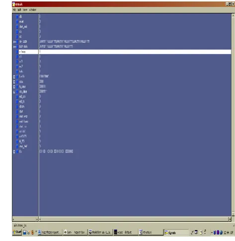
Fig 2. Synthesis of MAC Transmitter
[image:3.595.316.553.415.658.2]
Fig3. RTL view of complete MAC transmitter
Fig 3. shows the RTL view of MAC transmitter on clicking this block diagram it gives us internal block division of the MAC transmitter.
Fig4. Signal window of MAC transmitter S.
n
Parameters Total no. %tag
1 Number of slices 50 out of 192 26% 2 Number of slice flip flops 44 out of 384
11% 3 Number of 4 input LUTs 87 out of 384
22% 4 Number of bonded IOBs 17 out of 90
18% 5 Number of GCLKs 1 out of 04
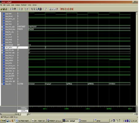
Fig5. Simulation waveform of MAC transmitter
[image:4.595.80.306.71.271.2]The data transmission by using MAC transmitter is as shown. In which the time period of mclkx 50 are 500, write signal is on low position(0) and reset is on high position(1). Now again changing the position of reset pin i.e. from 1 to 0 and make time period of txclk is 50, and then run the waveforms then data is shifted from Buffer to FSM and finally shifted to tx pin (4bit) with standard Frame data .From fig.6.4 On giving „0‟ value to reset it gives output as 0000, similarly on giving „1‟ value to reset and CD it gives output as ZZZZ, which is a don‟t care condition
.
Table 3 Analysis of different Control Signals
Sn SIGNALS RESET 0 RESET 1 CD 1
1 Clk 1 1 1
2 reset 0 1 1
3 Start_xmit 1 1 1
4 cs 0 0 0
5 cd 0 0 1
6 Src_addr 48 bit 48 bit 48 bit 7 Buff_data 32 bit 32 bit 32 bit
8 X_busy 1 0 0
9 RD 1 0 0
10 err1 0 0 0
11 err2 0 0 0
12 txdv 1 0 0
13 baddr 10001000 00000000 00000000
14 dout 0000 ZZZZ ZZZZ
15 tx_data 00001111 00000000 00000000 16 Crc_data 00001111 10101010 10101010
17 eof_crc 0 1 1
18 eof_tx 0 0 0
19 clken 0 0 0
20 start 1 0 0
21 xmit_over 0 0 0
22 xmit_fram 1 0 0
23 start_bo 0 0 0
24 rst_deff 0 0 0
25 cnt5120 1 1 1
26 id_95 0 0 0
27 start_deff 0 0 0
28 fcs 32 bit 32 bit 32 bit
7. CONCLUSION
The VHDL Implementation of MAC gives the improved digital design process, especially for FPGA design. A hardware description language allows a digital system to be designed and debugged at a higher level before conversion to the gate and flip-flop level. One of the most popular hardware description languages is VHISC hardware description language (VHDL) .It is used to describe and simulate the operation of variety IEEE 802.3 systems.
This paper has covered and discussed a software design, and implementation of a basic IEEE 802.3 (MAC Transmitter) system. The speed of data transmission is very high & it gives proper CRC bit for receiving correct data. The simulated waveforms give the reliability of the VHDL implementation to describe the characteristics and the architecture of the designed MAC with embedded BIST. The simulated waveforms also have shown the observer how long the test result can be achieved by using the Built-In-Self-Test technique (BIST) is completed at 39.2ms using 25 MHz clock speed transmitting at 100 Mbps. Even though it seems not to be as fast as it should be when BIST is implemented (the receiver needs to wait the signal from the transmitter), the MAC Transmitter module still takes advantage of the 100% fault coverage. This is the most important thing that should not be left out by any designer to ensure the reliability of their design. The next target for this research is to verify the RTL, implement and download it on Xilinx‟s FPGA chip.
8. REFERENCE
[1]Dr. M.S. Sutaone “Performance Evaluation of VHDL Coding Techniques for Optimized Implementation of IEEE 802.3” IEEE transaction on communication, pp- 287-293,Jan 12, 2008
[2]Fedrico Cali, Marco Conti, and Enrico Gregori “ IEEE 802.11 protocol: design and performance evaluation of an adaptive Back off mechanism” IEEE journal on selected areas in communications, vol .18.No.September 2000,pp1774-1778.
[3]P.M.Soni and a Chockalingam “IEEE analysis of link layer backoff schemes on Point –to-point Markov fading links” ,IEEE Transaction on communication, vol.51,no.1, January 2003,pp 29-31.
[4]IEEE 802.3 Cyclic Redundancy Check, Xilinx, XAPP209 (v1.0) march 23, Application note: vertex series and vertex II family, 2001, Author by Chriss Borelli
[5]Kenneth J.Christensen “A simulation study of enhanced arbitration methods for improving Ethernet performance” computer communications,21(1998)24-36, ELSEVIER.
[6]Douglas J. Smith ”HDL Chip Design A Practical Guide for designing ,synthesis & simulating ASICs & FPGAs using VHDL or Verilog”,3rd edition – MGH.pp179-183 and 198-201.
[7]Neil H.E.Weste and David Harris, ”CMOS VLSI Dsign A circuitand systems perspective”3rd edition – PIE,pp164-166.
8. AUTHORS BIOGRAPHY
Puran Gour has received his B.E. from amravati university Maharashtra and M.Tech from MANIT Bhopal and currently working as a Assistant Professor in NRI Institute of Information science and technology Bhopal (INDIA).He has over eight years teaching experience. His research interest in wireless communication and Microwave.
Ravi Shankar Mishra has received his M.Tech. degree from M.A.N.I.T. Bhopal(INDIA). He did PG diploma in VLSI design from C-DAC Bangalore. He is presently Ph.D. scholar at M.A.N.I.T. Bhopal. He has guided several M.Tech theses on communication field.