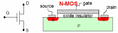
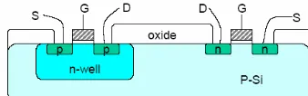
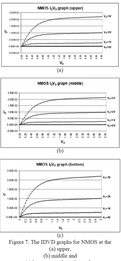
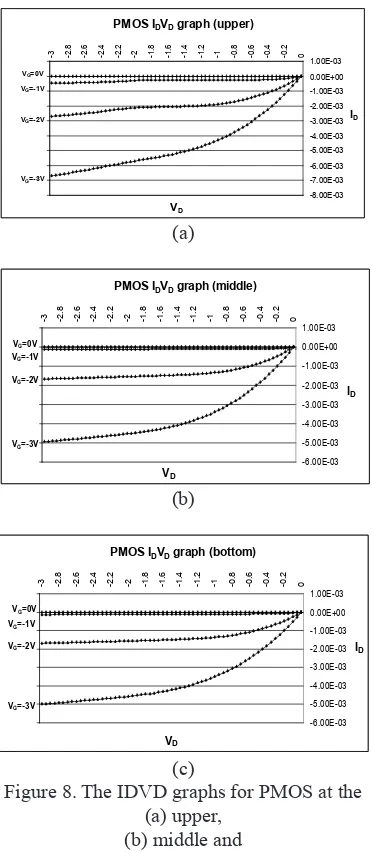
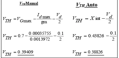
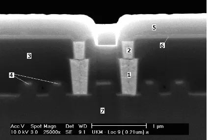
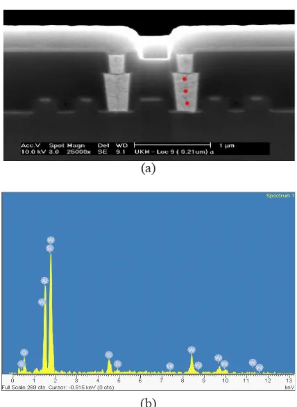
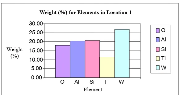
Device characterization of 0 21μm CMOS device
Full text
Figure
Related documents
Based on the perception, the organization will identify the right approach towards the BPR implementation and develop relevant appropriate plans for smooth and
In this study, riverbed sediments taken from the Yangtze mainstream and its major tributaries were analyzed in terms of their ESR signal intensity and CI values of quartz in
This framework utilised twelve substantial influences of brand loyalty and they include: brand commitment; brand affect; brand relevance; perceived value;
Vertex Edge Arc (directed edge) Weight (cost) Graph Weighted Graph Digraph 2 6 1 2... Introduction to
There was no significant difference between the two cowpea varieties, planting distance, spraying regime, variety × planting distance and variety × spraying
After applying the face detection and feature extraction to all images in the dataset, a dataset containing all features of all faces in the dataset has been
Free Download Write Can anyone know an app for download named - Windows Central Hours exe NT Kernel Disbursement Atmosphere Corporation ZwOpenObjectAuditAlarm 0x805F2C16
observations - can be used to compare distributions between sets of observations - observations may be discrete (underlying continuous) and continuous,. scatterplot - use to look
