A Single Nanoscale Junction with Programmable
Multilevel Memory
Curtis O'Kelly, Jessamyn A. Fairfield, and John J. Boland* School of Chemistry, Trinity College Dublin, Dublin 2, Ireland CRANN Institute, Trinity College Dublin, Dublin 2, Ireland Single Nanowire, TiO2, Memristor, Multilevel Memory
ABSTRACT: Nanoscale devices that are sensitive to measurement history enable memory applications,
and memristors are currently under intense investigation for robustness and functionality. Here we
de-scribe the fabrication and performance of a memristor-like device that is comprised of a single TiO2
nan-owire in contact with Au electrodes, demonstrating both high sensitivity to electrical stimuli and high
levels of control. Through an electroforming process, a population of charged dopants is created at the
interface between the wire and electrode that can be manipulated to demonstrate a range of device and
memristor characteristics. In contrast to conventional two-terminal memristors, our device is essentially
a diode that exhibits memristance in the forward bias direction. The device is easily reset to the off state
by a single voltage pulse and can be incremented to provide a range of controllable conductance states in
the forward direction. Electrochemical modification of the Schottky barrier at the electrodes is proposed
as an underlying mechanism, and six-level memory operations are demonstrated on a single nanowire.
Transition metal oxides are an emerging candidate material for the realization of non-volatile, low power
memory devices for handheld and portable electronics.1, 2 Non-volatile memories that retain encoded
in-formation without power consumption would greatly enhance battery performance for all mobile
plat-form technologies.3 Recent devices based on transition metal oxides display many characteristics required
2
has been the focus of much research since it was predicted to enable a specific type of RRAM operation
known as memristance.10 In principle, a memristive device can operate along a continuum of resistance
states between the traditional high resistance state (HRS) and low resistance state (LHS) found in
con-ventional resistive switching devices, with the evolution of the resistance state controlled by the flow of
charge through the device.11 In practice, the level of performance has yet to match that described in the
memristor simulations.12, 13 However, if reliability can be improved, memristors have the potential to
en-able novel multilevel or multibit coding paradigms, storing more information per unit memory cell and
maintaining this information without consuming power. Although a variety of multilevel memory devices
have been proposed,14, 15 it has proven difficult to program the number of levels with high fidelity and a
large on/off ratio.
To date, resistive switching and memristance have been demonstrated in planar thin film devices in which
the controlled resistance is achieved by the action of charged mobile dopants within the active device
layer.16-19 The conventional memristor is a two-terminal device in which a nanoscale film of active
mate-rial (TiO2 in this case) is sandwiched between metal electrodes. In this report, we use a TiO2 nanowire as
the active device material and demonstrate that a single electrical contact to this wire can be engineered
to create a memristor with unique performance characteristics. We show that in addition to the controlled
evolution of the current levels and hence the conductance of the device, it is possible to reset the device
by the application of a single voltage pulse, and to precisely increment the conductance states of the device
to implement multilevel memory that is more robust and reliable than has previously been shown in TiO2.
We show that our device effectively operates as a unipolar memristor diode, and discuss plausible
mech-anisms of device operation and advantages over conventional planar two terminal structures.
RESULTS AND DISCUSSION
Each device consisted of a single crystal TiO2 nanowire and two Au contacts, as shown in Figure 1(a).
Whereas the device is initially symmetric, in all subsequent processing steps one of the electrodes is held
3
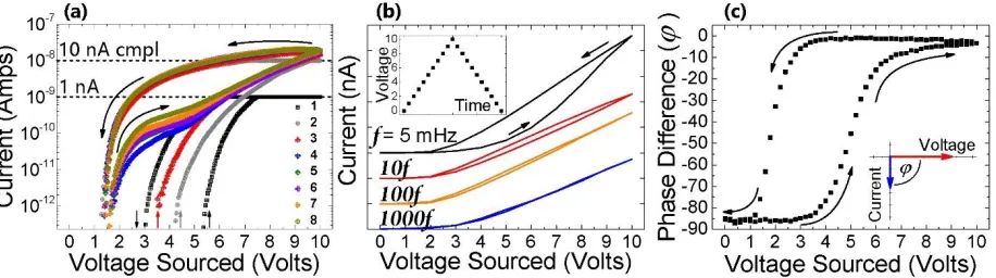
the initial state of the virgin device, a +10 V sweep is applied at a rate of 0.23 V/s (total time ~130 s)
while the current levels are monitored. Current typically ranges from 10–1000 pA for individual devices.
The black curve in Figure 1(b) shows a typical current trace for a virgin device. The current rises above
the noise threshold level at around +7 V during the initial voltage sweep, and there is clear hysteresis in
the current trace as the bias is swept to +10V and then back to 0V. The direction of the hysteresis loop is
indicated by the arrows in Figure 1(b).
The current levels within the nanowire device can be significantly increased by undergoing an
electro-forming step similar to those used for planar thin film TiO2 devices.16, 17, 20 This involves the application
of a steady state voltage (typically +10V) for a sustained time period (typically 1000 s) while the current
is monitored with a set compliance limit of 1 nA. The red curve in Figure 1(b) shows the difference in
current levels for the same device before and after the forming step. The maximum current is increased
and the turn-on voltage is reduced to +1.5V, comparable to the turn-off voltage for the device in its virgin
state. This electroforming step changes the properties of the wire in the vicinity of the positively biased
electrode (see below) and increases the overall conductance of the device. Similar behavior is observed
for a device under negative bias conditions, except that the modification of the wire occurs at the electrode
that is grounded (see Supporting Information Figure S2).
Current levels within the device can be developed further by successive electroforming steps at higher
set compliance values or through continuous and repeated application of voltage sweeps. Continuous
voltage sweeps reveal the dynamic behavior of the nanowire device and also provide insight into the
physical mechanism of operation. Figure 2(a) shows the evolving current response to a series of 8 voltage
sweeps. The conductance of the device increases incrementally with each applied sweep, up to a
maxi-mum conductance value. By the 8th sweep, the current levels no longer increases with additional voltage
sweeps, and the device response collapses into a stable repeating hysteresis loop. The turn-on and off
voltages also collapse onto a single value, +1.5 V in this case. Under this condition, the device remains
4
voltage sweeps. The SS condition provides a useful reference state for the device and to which the device
can always be returned. This is important for a dynamic memristor-like device which, by its nature, is
susceptible to changing state in response to the voltage, current, and sweep rate conditions it is exposed
to. The SS represents a stable reproducible state in an otherwise dynamic and continuously evolving
device operation space.
Changing the frequency of the applied voltage sweep also greatly affects the electrical properties of the
device, as seen in Figure 2(b). In each instance the device was brought to the SS associated with that
frequency. The different traces in the figure have been offset for clarity. The maximum sweep rate is 5
Hz, which is slow but reflects the > 2 µm size of the device. Altering the frequency of the applied voltage
sweep affects two aspects of the device current-voltage response. Firstly the maximum current becomes
diminished for faster voltage sweeps while secondly, the breath of the hysteresis loops become notably
collapsed at higher frequencies. Both behaviors are characteristic properties of memristors as described
by Chua and Williams et al, despite the fact that our device does not have the conventional two-electrode
sandwich memristor geometry.10, 11
Figure 2(c) shows the phase angle between the drive voltage and current recorded during the
measure-ment of the SS in Figure 2(a). A phase angle of -90 degrees is consistent with a capacitive response that
dominates the initial low voltage behavior of the device, however at larger voltages the response is
resis-tive indicating the establishment of improved electrical conduction between wire and the metal contact.
This behavior is consistent with the presence of a blocking capacitor at the device interface that becomes
increasingly transparent at high applied voltages.
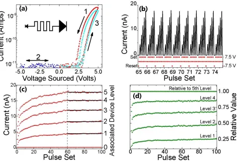
Figure 3(a) shows the response of a device specifically prepared to be in the SS to a bipolar voltage
sweep. As expected, the device initially displays the SS response during first positive voltage sweep (red
curve labeled 1 in figure), similar to the response seen in Figure 2(a). On the other hand, no significant
level of current is observed during the negative voltage sweep (2), indicative of diode-like behavior. The
5
the first sweep. Our device is therefore essentially a unipolar memristor, and thus the application of a
negative voltage pulse can be used to systematically step back or reduce the conductance at positive
bi-ases. Note however that the application of a sustained negative voltage eventually quenches the device
conductance in the positive voltage direction, resulting in the growth of the same device characteristic
seen in Figure 2, except at negative voltages with the electroforming phenomenon at the grounded
elec-trode (see Figure S2).
This ability to reset or step back the conductance in the forward channel by applying a reverse bias pulse
is not available in conventional memristors and enables improved control of device operation and
en-hanced performance. Thus we can apply a -7.5V pulse to reset the device, following which we examine
the device response to a subsequent series of positive set pulses. Figure 3(b) shows the combined effect
of a -7.5 V reset followed by five +7.5 V set pulses for a device that was originally in its SS defined by a
18 nA saturation current at +7.5 V. The pulse width is 2.5 sec in duration. Each positive voltage pulse
increments the device conductance by a specific amount while the device can be quantitatively reset using
a negative pulse. The resulting six-level memory device in Fig 3(b) has high current fidelity and precisely
controlled levels compared to previous multilevel memory devices.21, 22 The observed on-off ratio is
ex-cellent, as expected for high-purity TiO2.15 Figure 3(c) shows the time evolution of the six-level memory
device from the beginning of the pulsing sequence. We note that the device response evolves during the
initial cycles but beyond 60 pulse applications it saturates into six well defined conductance levels, from
which the data in Fig. 3(b) was recorded. This initial behavior is consistent with that seen earlier in Figure
2(a) and typical of memristor devices in general,10 which exhibit a temporal response to any voltage
stim-ulus. Critically, the relative separation between the memory levels remains unchanged even during the
initial period. This is underscored in Fig 3(d) which shows the magnitude of the current at each level as
a fraction of the highest current level. Despite the initial induction period the relative magnitudes are
essentially constant throughout. Once steady state has been achieved the conductance values associated
with each memory level are defined to better than 3%. By changing the pulse combination or by tuning
6
that span the maximum current level the device can support. Supporting Figure S3 shows the case of a
four-level memory device. The status of the multilevel memory levels is read by the application of a
sub-threshold voltage pulse large enough to produce a measurable current, but not capable of modifying the
conductance. Threshold behavior is a characteristic memristor property and in our case the optimum read
pulses are between +3 V and +5 V.12
The mechanism of resistive switching and memristance in TiO2-based device is widely debated in the
literature.23 Here we hypothesise on the operation of our device in the context of what has been reported.
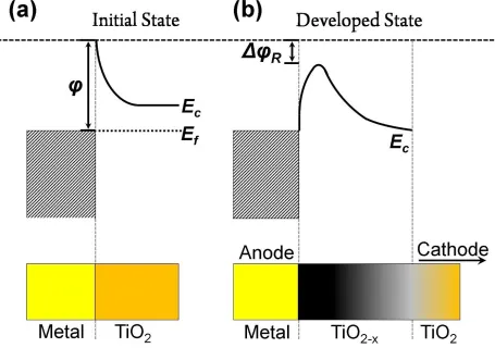
We begin by considering the band alignment across the device structure shown in Figure 1(a). The Au
contact leads have a work function of 5.1 eV and form Schottky barrier contacts with the wide bandgap
TiO2 nanowire. Since the nanowire is single crystal with a high degree of perfection, few carriers are
available to screen the Schottky barrier, so that the presence of the latter likely dominates the measured
conductance of the virgin wire. This situation is described schematically in Figure 4(a) where band
bend-ing reflects the Schottky barrier height and width. Under electroformbend-ing conditions described here
oxy-gen vacancies are known to readily form at the TiO2 interface with the positively biased Au metal
con-tact.16, 17, 20, 24, 25 These anodic conditions result in the oxidation of the lattice oxygen 𝑂
𝑂× to form positively
charged oxygen vacancies 𝑉𝑂•• by the following reaction:26
𝑂𝑂× ⇄ 𝑉
𝑂••+ 2𝑒′+12𝑂2 (𝑔) (1)
It is well established that oxygen vacancies act as n-type dopants with shallow donor states below the
conduction band of bulk TiO2.27 This has the effect of shifting the Fermi energy closer to the bottom of
the TiO2 conduction band, as shown in Figure 4(b), thereby increasing the number of free electrons in the
band. The oxygen vacancies generated by reaction (1) may form a charged double-layer with the negative
sheet of charge on the Au electrode established during Schottky barrier formation.26 This double layer is
7
The additional carriers created by this reaction will reduce the Schottky barrier height and width and
increase the rate of tunneling into the contact. If a sufficiently large population of vacancy dopants are
created and extend beyond the interface, an impurity band could form that facilitates conduction by a
variable range hopping mechanism.28
An important aspect of the device operation is that positively-charged oxygen vacancies that are created
at the anode are mobile. While mobility is necessary to establish the charge double layer described above,
any penetration of an applied electric field through the double layer will naturally cause the oxygen
va-cancies to drift away towards the cathode. Based on this we suggest that the SS condition described in
Figure 2(a) reflects a balance between the rate of vacancy generation at the anode and the rate of vacancy
drift towards the cathode. Crucially, the application of a short negative (reset) voltage pulse has the effect
of injecting electrons from the Au electrode into the wire, annihilating oxygen vacancies in the near
con-tact region via the reverse of reaction (1). This creates a depletion region next to the Au electrode and
effectively resets the device, consistent with the data in Figure 3. Subsequent set pulses sequentially
restore the oxygen vacancy population. This unique reset ability provides an important handle in
control-ling the multilevel memory operation.
The device reported here has parallels with conventional planar Au/TiO2/Au memristors, except that by
comparison the thickness of the TiO2 layer in this device is very large, which effectively separates the
behavior of the device at the two electrode regions so that they can be treated independently. In contrast,
a conventional planar memristor typically has an oxide layer that ranges in thickness from 20-50 nm, and
both electrodes are involved in the creation and/or subsequent reaction of mobile charge dopants
respon-sible for device operation. Issues such as dopant discharge at the counter electrode are common.12 An
obvious attraction of the device geometry in Figure 1(a) is the possibility of gating. Whilst this is not
important in the present case—the channel length is 2 µm and the overall conductance of the device is
8
length is reduced, allowing modulation of the tails in the barriers that extend into the channel from the
electrode regions on either side.
CONCLUSIONS
In conclusion, we demonstrate a memristor-diode device in which a population of charged dopants can be
created and manipulated. The device exhibits all the hallmarks of a memristor but has the advantage of a
well-defined saturated state, a reference to which the device can always be returned. Moreover, the device
can be reset into an off-state that is well defined with respect to the saturated state and from which its
conductance can be controllably evolved into a precision multilevel memory.
METHODS
Single nanowire devices are fabricated following a three step process of UV lithography that involves defining contact pads, nanowire spray deposition, and electron beam lithography (EBL) to define metal contacts to the wires. Devices were fabricated on silicon substrates with 200 nm oxide thickness. UV lithography was used to produce 150 µm2 Ti/Au metal contact pads with thickness 5/30 nm, respectively. Dilute solutions of commercially available TiO2 wires (EMFUTUR) dispersed in deionized water were then hand-sprayed onto the substrate. EBL was used to draw Au metal contacts 80 nm thick to each indi-vidual nanowire such that only Au metal was in contact with the wires. The physical dimensions of the TiO2 nanowires are between 50-100 nm in diameter and 5-20 µm in length. Transmission electron mi-croscopy confirmed the crystallographic structure of the single crystal anatase TiO2 nanowires (see Sup-porting Information Figure S1).
9
Figures and Captions.
Table of Contents Graphic
10
11
12
[image:12.612.77.532.84.404.2]13
AUTHOR INFORMATION
Corresponding Author
*E-mail: [email protected]. Phone: +353 1-896-3140.
Funding Sources
The authors wish to acknowledge funding from the European Research Council under Advanced Grant 321160. This publication has emanated from research supported in part by a research grant from Science Foundation Ireland (SFI) under Grant Number SFI/12/RC/2278). J.A.F. acknowl-edges funding from the Irish Research Council EMPOWER Fellowship.
ACKNOWLEDGMENT
The authors wish to thank the Advanced Microscopy Laboratory at Trinity College Dublin for assistance with electron microscopy and characterization.
Supporting Information. High-resolution transmission electron microscopy, selected area elec-tron diffraction, and fast Fourier transforms of the nanowires used in these devices are shown in the supporting information. Device operation under negative bias and a 4 level memory device are also presented along with a comment on device yield. This material is available free of charge via the Internet at http://pubs.acs.org.
References
1. Jeong, D. S.; Thomas, R.; Katiyar, R. S.; Scott, J. F.; Kohlstedt, H.; Petraru, A.; Hwang, C. S., Emerging memories: resistive switching mechanisms and current status. Rep. Prog. Phys.
2012,75, 076502.
2. Sawa, A., Resistive switching in transition metal oxides. Mater. Today 2008,11, 28-36. 3. International Technology Roadmap for Semiconductors 2013 Edition.
http://www.itrs.net/Links/2013ITRS/Summary2013.htm.
4. Cui, Y.; Peng, H.; Wu, S.; Wang, R.; Wu, T., Complementary charge trapping and ionic migration in resistive switching of rare-earth manganite TbMnO(3). ACS Appl. Mater. Interfaces
2013,5, 1213-1217.
5. Nardi, F. B., S. Larentis, S. Gilmer, D. Lelmini, D., Complementary switching in oxide-based bipolar resistive-switching random memory. IEEE Trans. Electron Devices 2013,60. 6. Park, G. S.; Kim, Y. B.; Park, S. Y.; Li, X. S.; Heo, S.; Lee, M. J.; Chang, M.; Kwon, J.
14 7. Huang, Y. T.; Yu, S. Y.; Hsin, C. L.; Huang, C. W.; Kang, C. F.; Chu, F. H.; Chen, J. Y.;
Hu, J. C.; Chen, L. T.; He, J. H., et al., In situ TEM and energy dispersion spectrometer analysis of chemical composition change in ZnO nanowire resistive memories. Anal. Chem. 2013,85,
3955-3960.
8. Hsu, C.-H.; Fan, Y.-S.; Liu, P.-T., Multilevel resistive switching memory with amorphous InGaZnO-based thin film. Appl. Phys. Lett. 2013,102, 062905.
9. Y. Shuai, X. O., W. Luo, N. Du, C.Wu,W. Zhang, D. Bürger, C.Mayr, R. Schüffny, S. Zhou, M. Helm, and H. Schmidt, Nonvolatile multilevel resistive switching in Ar+ Irradiated
BiFeO3 thin films. IEEE Trans. Electron Devices 2013,34.
10. Strukov, D. B.; Snider, G. S.; Stewart, D. R.; Williams, R. S., The missing memristor found. Nature 2008,453, 80-83.
11. Chua, L., Resistance switching memories are memristors. Appl. Phys. A 2011,102, 765-783.
12. Yang, J. J.; Strukov, D. B.; Stewart, D. R., Memristive devices for computing. Nat. Nanotechnol. 2013,8, 13-24.
13. Pershin, Y. V.; Di Ventra, M., Memory effects in complex materials and nanoscale systems. Adv. Phys. 2011,60, 145-227.
14. Chu, H.-L.; Chiu, S.-C.; Sung, C.-F.; Tseng, W.; Chang, Y.-C.; Jian, W.-B.; Chen, Y.-C.; Yuan, C.-J.; Li, H.-Y.; Gu, F. X., et al., Programmable Redox State of the Nickel Ion Chain in
DNA. Nano letters 2014,14, 1026-1031.
15. Hu, C.; McDaniel, M. D.; Posadas, A.; Demkov, A. A.; Ekerdt, J. G.; Yu, E. T., Highly Controllable and Stable Quantized Conductance and Resistive Switching Mechanism in
Single-Crystal TiO2 Resistive Memory on Silicon. Nano Lett. 2014.
16. Jeong, D. S.; Schroeder, H.; Breuer, U.; Waser, R., Characteristic electroforming behavior in Pt/TiO2/Pt resistive switching cells depending on atmosphere. J. Appl. Phys. 2008,
104, 123716.
17. Joshua Yang, J.; Miao, F.; Pickett, M. D.; Ohlberg, D. A.; Stewart, D. R.; Lau, C. N.; Williams, R. S., The mechanism of electroforming of metal oxide memristive switches.
Nanotechnology 2009,20, 215201.
18. Salaoru, I.; Khiat, A.; Li, Q.; Berdan, R.; Papavassiliou, C.; Prodromakis, T., Origin of the OFF state variability in ReRAM cells. J. Phys. D: Appl. Phys. 2014,47, 145102. 19. Du, Y.; Pan, H.; Wang, S.; Wu, T.; Feng, Y. P.; Pan, J.; Wee, A. T. S., Symmetrical Negative Differential Resistance Behavior of a Resistive Switching Device. ACS Nano 2012,6,
2517-2523.
20. Kwon, D. H.; Kim, K. M.; Jang, J. H.; Jeon, J. M.; Lee, M. H.; Kim, G. H.; Li, X. S.; Park, G. S.; Lee, B.; Han, S., et al., Atomic structure of conducting nanofilaments in TiO2
resistive switching memory. Nature nanotechnology 2010,5, 148-153.
21. Choi, S. J.; Park, G. S.; Kim, K. H.; Cho, S.; Yang, W. Y.; Li, X. S.; Moon, J. H.; Lee, K. J.; Kim, K., In situ observation of voltage-induced multilevel resistive switching in solid
electrolyte memory. Adv. Mater. 2011,23, 3272-3277.
22. Iulia, S.; Ali, K.; Qingjiang, L.; Radu, B.; Christos, P.; Themistoklis, P., Origin of the OFF state variability in ReRAM cells. Journal of Physics D: Applied Physics 2014,47, 145102.
23. Waser, R.; Dittmann, R.; Staikov, G.; Szot, K., Redox-Based Resistive Switching Memories - Nanoionic Mechanisms, Prospects, and Challenges. Adv. Mater. 2009,21,
2632-2663.
15 25. Kazuki, N.; Takeshi, Y.; Masaki, K.; Keisuke, O.; Annop, K.; Sakon, R.; Gang, M.; Mati,
H.; Bo, X.; Fuwei, Z., et al., Switching Properties of Titanium Dioxide Nanowire Memristor. Jpn. J. Appl. Phys. 2012,51, 11PE09.
26. Jeong, D. S.; Schroeder, H.; Waser, R., Mechanism for bipolar switching in a TiO2 resistive switching cell. Phys. Rev. B 2009,79, 195317.
27. Janotti, A.; Varley, J. B.; Rinke, P.; Umezawa, N.; Kresse, G.; Van de Walle, C. G., Hybrid functional studies of the oxygen vacancy in TiO2. Phys. Rev. B 2010,81. 28. Fogler, M. M.; Teber, S.; Shklovskii, B. I., Variable-range hopping in
quasi-one-dimensional electron crystals. Phys. Rev. B 2004,69, 035413.
29. Keithley, Performing Very Low Frequency Capactiacne-Voltage Measurements on High Impedance Devices Using the Model 4200-SCS Semiconductor Characterization System.