© 2016, IRJET ISO 9001:2008 Certified Journal Page 1930
Design and analysis of SRAM cell for ULP application
Harsh Vardhan Kumar
1,Owais shah
21M.Tech. VLSI, Noida International University, Greater Noida, UP, India
2Asst. professor, Noida International University, Greater Noida, UP, India
---***---Abstract-The rapid advancement in processors, controllers, digital system and portable electronic system demands
ultra low power consumption. The above devices consist almost 2/3rd of VLSI circuits as SRAM (Static Random Access Memory), leads majority of power consumption into the ciruit.Now there is necessity to focus on SRAM to minimize the power consumption. This paper focuses on the power dissipation during the write, read and hold operation in 4T, 5T, 6T, 7T, 8T and 9T CMOS SRAM cells. These SRAM circuits are drawn simulated on Tanner EDA Tool 13.0[11] at different technologies (16nm, 22nm and 32nm) varying the supply voltage VDD from 0.6V-1.3V[1].The average power consumption and Signal to Noise Margin (SNM)[2] of different SRAM cells are compared in different modes of operation at different technologies The results are compared among 4T, 5T, 6T,7T, 8T and 9T SRAM cell which are also being characterized in this thesis with the same technology.SNM(signal noise margin)plays an important role in SRAM stability, the comparative chart is also characterized with write, read and hold operation.
Keywords: Ultra low Power, SNM,SRAM, 16nm,22nm,32nm,4T,5T,6T, 7T,8T,9T SRAM cell.
1. INTRODUCTION
The capability of handling data in chips named as memory. Static random access memory (SRAM) holds one bit of information using bi-stable circuitry. A SRAM can be designed by NMOS and PMOS transistors in CMOS technology [3]. The transistors are scaled down which also increases leakage currents and it reduces the battery life. In order to reduce the leakage current additional transistors can be added to conventional 6T SRAM [1] to have low power consumption. It reduces these adverse effects in the basic SRAM cell performance and 4T, 5T SRAM can be used for cache memory. We will observe a couple of SRAM Cells that allow the analysis and simulations of the power dissipation and signal to noise margin (SNM) [2]at 32nm, 22nm and 16nm technology[5].
1.1Static Random-Access Memory (SRAM)
© 2016, IRJET ISO 9001:2008 Certified Journal Page 1931
Fig. 1: 4T SRAM cell Fig. 2: 6T SRAM cell
An SRAM cell has three different states i.e. write operation (updating the contents), hold operation (the circuit is idle) and read operation (the data has been requested). The SRAM operates in read mode and write mode. The three different states of SRAM cell work as follows.
1.1.1 Hold operation
When word line voltage is kept at logic 0 the access transistors disconnect the memory cell from bit lines(BL and BLB) and two cross-coupled inverters (M1-M4 and M2-M3)continues to reinforce one another till power supply is given. These operations is assumed when there is no read and write operation of memory cell and it is also important to retain the content of memory and in power analysis of the circuit.
1.1.2 Read operation
In this operation either logic 0 or 1 to be sensed from SRAM cell through Q and QB.Assuming the content of the memory cell at Q is logic 1. Pre-charge both the bit lines (BL and BLB) to logic 1 then provide voltage to the word line WL to enable the access transistors. Now value stored at Q and QB will be transferred through BL and BLB.Since Q is at logic 1 BL will remain at logic 1 and BLB will discharge through M1 and M5. If the content of the memory is logic 0, the opposite operation will occur and BLB will charge to logic 1 and BL towards logic 0. Beside of very small voltage difference in BL and BLB sense amplifier senses whether BL or BLB have higher voltage. If sense amplifier senses higher voltage at BL then memory at logic 1 and vice versa. The sensing response of sense amplifier will decide the speed of SRAM cell.
1.1.3Write operation
The write operation starts what we supposed to write into memory. If we wish to write logic 0, we must apply voltage to bit lines (BL to logic 0 and BLB to logic 1). This is as similar as applying a reset pulse to an SR flip-flop, causes the flip flop to change the logic level. If we wish to write 1, we must invert the logic state of bit lines (BL to logic 1 and BLB to logic 0). Word line voltage (WL) is asserted to logic 1 at both the above operation. The driver transistors are kept higher (W/L ratio) than load transistors so that overriding can be done quickly in cross coupled inverters. But this may lead more power loss.
1.2 Different SRAM cells
© 2016, IRJET ISO 9001:2008 Certified Journal Page 1932
1.2.1 4T SRAM cell
Figure.3 shows 4T SRAM cell in which four transistors are used as a memory cell and pull up transistors are implemented by extra layer of polysilicon. This results high resistance pulls up transistors and finally more power consumption. Two transistors are used as access transistor. Even though it is commonly used as cache memory. It operates in different modes same as conventional 6T SRAM cell.
Fig. 3 4T SRAM Cell
1.2.2 5T SRAM Cell
Figure.4 is 5T SRAM cell consists of five transistors. There is only one access transistor which is accessed by bit line BL.The operation of SRAM cell is controlled by bit line voltage BL and is as similar the operation of 6T SRAM cell and quite commonly used as CPU caches in SRAM devices.
[image:3.596.149.464.247.424.2] [image:3.596.118.482.573.763.2]© 2016, IRJET ISO 9001:2008 Certified Journal Page 1933
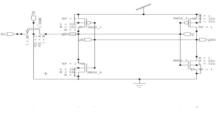
[image:4.596.157.420.298.354.2]1.2.3 6T SRAM Cell
Figure.5. shows the circuit of 6T SRAM cell [1]and consists of six transistors. The construction and working in three different modes (write, read and hold operation) of the circuit is explained above. It is conventional SRAM cell which is commonly used as memory. It operates in three different modes write, read and hold operation. These are explained as above in SRAM theory.
Fig. 5: 6T SRAM Cell
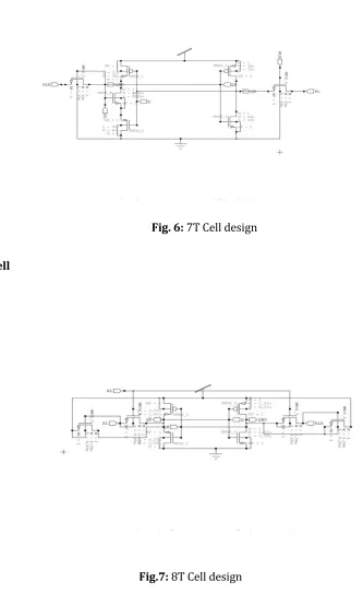
1.2.4 7T SRAM cell
© 2016, IRJET ISO 9001:2008 Certified Journal Page 1934
Fig. 6: 7T Cell design
1.2.5 8 T SRAM cell
Fig.7: 8T Cell design
Figure.7. is the architecture 8T SRAM cell[7]. Two extra transistors are added as compared to 6T SRAM cell. One transistor is used to reduce gate leakage current and other transistor is used to maintain SNM of the memory cell in the zero state. Word line (WLB) signal is the complement of word line (WL) signal. Timing diagram of signal WL and WLB in different mode of operation is shown below in figure.8.The operation of 8T SRAM cell is controlled by single end sense amplifier. The operation of 8T SRAM cell can be implemented by adding additional
© 2016, IRJET ISO 9001:2008 Certified Journal Page 1935
Fig. 8: Timing Diagram of 8T SRAM cell
1.2.69T SRAM cell
Figure.9. is the architecture of 9T SRAM cell[8]. It consists of 03 extra transistors with conventional cell as shown in Figure 9.The extra transistors gives complexity to the circuit but have stable SNM in read operation. It may lead to extra power consumption. One more transistor is added to 8T SRAM cell to pulls down cross coupled inverters and one more pulse voltage is required to control the leakage current [6] to the circuit. The operation of 9T SRAM cell can be implemented by adding pulse voltage (RWL and WLB) into conventional 6T SRAM cell.
Fig. 9: 9T SRAM cell
© 2016, IRJET ISO 9001:2008 Certified Journal Page 1936
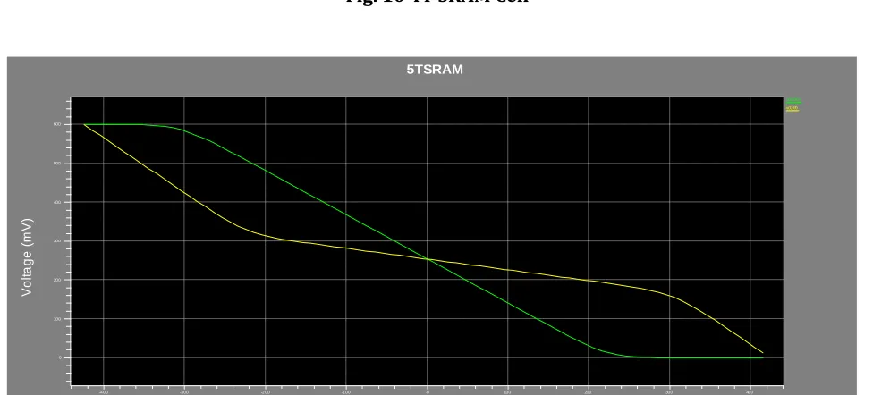
-400 -300 -200 -100 -0 100 200 300 400
[image:7.596.55.523.98.313.2]U (m) 0 50 100 150 200 250 300 350 400 450 500 550 600 V o lt a g e ( m V ) v(Q BD) v(Q D) 4TSRAM
Fig. 10 4T SRAM Cell
-400 -300 -200 -100 -0 100 200 300 400
U (m) 0 100 200 300 400 500 600 V o lt a g e ( m V ) v(Q BD) v(Q B) 5TSRAM
[image:7.596.54.542.339.560.2]© 2016, IRJET ISO 9001:2008 Certified Journal Page 1937
-400 -300 -200 -100 -0 100 200 300 400
U (m)
0 100 200 300 400 500 600
V
o
lt
a
g
e
(
m
V
)
v(Q BD)
[image:8.596.52.518.97.315.2]v(Q B) 6TSRAM
Fig. 12 6T SRAM Cell
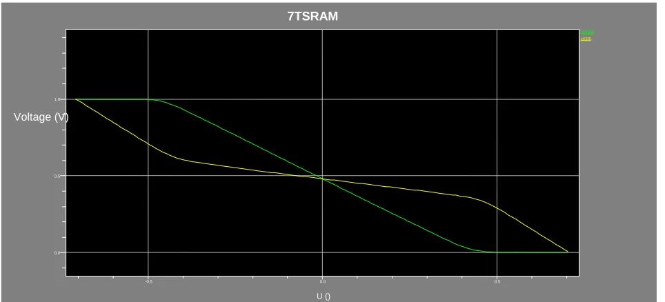
Fig. 13 7T SRAM Cell
-0.5 0.0 0.5
U () 0.0
0.5 1.0
Voltage (V)
v(QBD)
v(QB)
[image:8.596.57.539.369.588.2]© 2016, IRJET ISO 9001:2008 Certified Journal Page 1938
-500 0 500
[image:9.596.50.524.101.314.2]U (m) 0.0 0.5 1.0 V o lt a g e ( V ) v(Q BD) v(Q B) 8TSRAM
Fig. 14 8T SRAM Cell
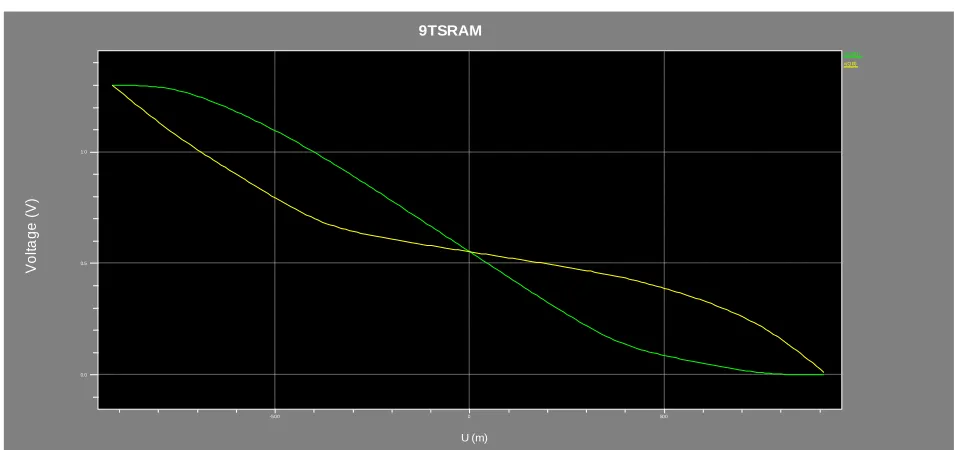
-500 0 500
[image:9.596.56.537.365.590.2]U (m) 0.0 0.5 1.0 V o lt a g e ( V ) v(Q BD) v(Q B) 9TSRAM
Fig. 15 9T SRAM Cell
3. CONCLUSIONS
© 2016, IRJET ISO 9001:2008 Certified Journal Page 1939
3.1Comparison of average power consumption and SNM of different SRAM cells at 16nm
Chart-1 Power consumption(write operation)
Chart-2 SNM(write operation)
Chart-3 1 Power consumption(read operation)
Chart-4 SNM(read operation)
© 2016, IRJET ISO 9001:2008 Certified Journal Page 1940
3.2Comparison of average power consumption and SNM of different SRAM cells at 22nm
Chart-7 Power consumption(write operation) Chart-8 SNM (write operation)
Chart-9 Power consumption(read operation)
0 0.2 0.4 0.6 0.8 1 1.2 1.4
0.6 0.7 0.8 0.9 1 1.1 1.2 1.3
4T
5T
6T
7T
8T
9T
Chart-10 SNM(read operation)
Chart-11 Power consumption(hold operation)
© 2016, IRJET ISO 9001:2008 Certified Journal Page 1941
3.3Comparison of average power consumption and SNM of different SRAM cells at 32nm
Fig. 22 Power consumption(write operation) Fig. 23 SNM (write operation)
Fig. 24 Power consumption(read operation) Fig. 25 SNM(read operation)
0
0.00001
0.00002
0.00003
0.00004 0.00005 0.000060.6 0.7 0.8 0.9 1 1.1 1.2 1.3
4T
5T
6T
7T
8T
9TFig. 26 Power consumption(hold operation)
0 0.2 0.4 0.6 0.8 1 1.2 1.4
0.6 0.7 0.8 0.9 1 1.1 1.2 1.3
4T 5T 6T 7T 8T 9T
Fig. 27 SNM(hold operation)
[image:12.596.34.514.130.706.2]© 2016, IRJET ISO 9001:2008 Certified Journal Page 1942
REFERENCES
[1] Jawar Singh, Dhiraj K.Pradhan,” A single ended 6T SRAM cell design for ultra low voltage applications”, IEICE Electronic Express, 2008, pp-750-755.
[2] Rajshekhar Keerthi ,Henry Chen, “Stability and static noise margin analysis of low power SRAM” IEEE International Instrumentation & Measurement Technology Conference, Victoria Canada, May 2008,pp-1541-1544.
[3] A.P.Chandrakasan, S. Sheng, and R. W. Brod ersen, “Low-power CMOS digital design.” IEEE J. Solid- State Circ., vol. 27, no. 4, pp. 473-484, Apr. 1992.
[5] Sapna Singh, Neha Arora, Meenakshi Suthar and Neha Gupta ‘Performance Evaluation of Different SRAM Cell Structures at Different Technologies’ February2012
[6] Narender Hachette and Nagarajan Ranganathan, "LECTOR: A technique for leakage reduction in CMOS circuits," IEEE Trans., on VLSI Systems, vol. 12, No.2, Feb 2004.
[7] Chang, L. Montoye, R.K. Nakamura, Y.Batson, K.A.Eickemeyer, R.J.Dennard, R.H. Haensch, W.Jamsek, D, “An 8T-SRAM for variability tolerance and low-voltage operation in high-performance caches”, Solid-State Circuits, IEEE Journal vol. 43, April 2008, Issue 4, p-956-963.
[8] Zhiyu Liu, Volkan Kursun, “ Characterization of a novel nine transistor SRAM cell”, IEEE Transactions on Very Large Scale Integration Systems,vol.46, Issue 4,April 2008.pp-488-492.
[9] Koichi Takeda , “A read static noise margin free SRAM cell for low Vdd and high speed applications”, Solid-State Circuits, IEEE Journal vol. 41, Jan.2006, Issue 1, pp.113-121.
[10] Rajshekhar Keerthi ,Henry Chen, “Stability and static noise margin analysis of low power SRAM” IEEE International Instrumentation & Measurement Technology Conference, Victoria Canada, May 2008,pp-1541-1544.
[11] Simaran Kaur, Ashwani Kumar ‘Analysis of Low Power SRAM Memory Cell using Tanner Tool’ IJECT Vol. 3, Issue 1, Jan. - March 2012
![Figure.5. shows the circuit of 6T SRAM cell [1]and consists of six transistors. The construction and working in three different modes (write, read and hold operation) of the circuit is explained above](https://thumb-us.123doks.com/thumbv2/123dok_us/8199605.815259/4.596.157.420.298.354/figure-consists-transistors-construction-different-operation-circuit-explained.webp)