International Journal of Emerging Technology and Advanced Engineering
Website: www.ijetae.com (ISSN 2250-2459, ISO 9001:2008 Certified Journal, Volume 7, Issue 12, December 2017)
271
Radiation Effects and Mitigation Techniques for
Space Electronics
S.Anitha
1*,T.Yugendra Chary
2*, Ameet Chavan
3* Assistant professor, ECE Department, Sreenidhi Institute of Science and Technology,Hyderabad
3
Professor, ECE Department, Sreenidhi Institute of Science and Technology,Hyderabad
Abstract—Space electronic devices are subjected to hostile
environment consisting of charged particles like proton, alpha and neutron. When these charged particles interact with electronic devices present in space, causes destructive and non-destructive effects. Total Ionization Dose and single Event Effect are the major problem in electronic devices, which are subjected to radiation. This paper describes the issues and impact of radiation on semiconductors (TID, SEE) and their mitigation techniques to be followed at different design levels. During Radiation, Charge Sharing is other major problem in Digital circuits. The effect of charge sharing and methods to avoid this problem is also discussed. This paper provides a snapshot of the problem related to radiations and some basic approaches to reduce these effects.
Keywords—Radiation Hardening, Single Event Effect (SEE), Charge Sharing, Total Ionization Dose (TID), Critical Charge, Linear energy Transfer, Common Centroid
I. INTRODUCTION
Radiation hardening is the process of making electronic systems resistant to damage or malfunctions caused by ionizing radiation such as those encountered in space or high altitude flights [1]. The Electronic Components present in Semiconductors are susceptible to radiation damage. Space radiations are more complex and energetic compared to terrestrial radiations. Particles which are highly charged and heavy energized ions which are present in Galactic cosmic rays cause greater damage to electronic devices. These particles have energy in the range of 100MeV -1GeV. Highly energetic protons which are emanates during solar flares are other form of particle which causes radiation [1-2]. If these ion particle hits a storage cell then the value of data stored in the cell may be flipped if the charge deposited by ion hit is greater than critical charge(amount of charge required to change the state of node). Where as in the combinational circuit this ion hit result in improper functioning and also alters the node characteristics. Radiating particle such as neutron and proton generates two types of effects on electronic devices they are:
1. Long term effects causing functional or parameter failures
Displacement Damage
Total Ionization Dose
2. Transient or Single particle effect Single Event Error
II. TOTAL IONIZATION DOSE
It is an undesired effect caused by interaction of electronic devices and radiation particle. Ionization refers to addition or removal of electrons from atom, which leads to creation of electron-hole pair. In TID effect, when a charge particle strikes the device it deposits the charge at oxide region and creates electron-hole pair. During the presence of electric field in oxide the electron-hole pair doesn‘t recombine, as they drift in the electric field. Electrons with higher mobility leave the oxide while the holes are trapped in the oxide region [1-2]. This process creates defects at oxide interface and leads to device degradation. The basic mechanism involved is:
Particle strike
Creation of electron-hole pair
Variations in VTH
Device degradation
International Journal of Emerging Technology and Advanced Engineering
Website: www.ijetae.com (ISSN 2250-2459, ISO 9001:2008 Certified Journal, Volume 7, Issue 12, December 2017)
272
mobility, Power consumption and Device degradation. Field isolation, Buried oxide leakage, and Technology variation are challenges of TID which can be reduced by different mitigation techniques like Shielding which reduces low energy protons and neutrons.
III. SINGLE EVENT ERROR
The other event which occurs due to interaction of semiconductors and radiating particle is Single Event Error. A dense track of E-H pair is generated by particle strike which causes a transient current pulse that degrades the device [1]. SEE is broadly classified into two types:
i. Hard Errors (SEGR)
ii. Soft Errors (SEU, SEL, SET)
Hard errors are non-recoverable; they cause permanent damage to the device operation. SEGR (single error gate rupture) is an effect in which gate oxide gets damaged and results in current path.
Soft errors are recoverable they don‘t cause any permanent damage to the device operation these errors can be restored by resetting or rewriting the information [6].
SEU (Single Event Upset): whenever a particle hits a sensitive node in a circuit the value present at that node gets flipped i.e. single event upset is a change of state of a node in the device. This effect is seen in storage elements.
[image:2.612.322.542.115.471.2]SET (Single Event Transient): Because of SEE a transient glitch is generated, which propagates through the combinational logic path and finally gets latched into storage element. Figure 1 explains effect of SEE and propagation of current pulse to output.
Fig 1: Single Event Effect
SEL (Single Event Latch): This is caused by the parasitic in bipolar circuits which results in high current state. Whenever a particle strikes the material it loses its energy. The amount of energy lost by the particle per unit length is called as linear energy transfer [7].
+
--
--
--
-+
+
+
+
+
+
+
+
+
+
+
+
+
+
+
+
-I
diff--
-- --
--
--
-
-+
+
+
+
+
+
+
+
+
+
+
+
+
++
+
+
+
+
+
+
+
+
+
+
+
+
+
I
driftn+
p-Si
-+
-
+-
+
+
-+
-
-
+-
+
+
-+
-
-
+-
+
+
-+
-
-
+-
+
+
-+
-
-
+-
+
+
-+
-
-
+-
+
+
-+
-
-
+-
+
+
-+
-
-
+-
+
-
-- --
-Ion track
a.) b.) c.)
0
1
2
3
10
-1310
-1210
-1110
-1010
-9Time (seconds)
Curr
e
n
t
(a
.u
.)
b.) Prompt chargecollection c.) Diffusion charge collection a.) Onset of event
+
--
--
--
-+
+
+
+
+
+
+
+
+
+
+
+
+
+
+
+
-I
diff--
-- --
--
--
-
-+
+
+
+
+
+
+
+
+
+
+
+
+
++
+
+
+
+
+
+
+
+
+
+
+
+
+
I
driftn+
p-Si
-+
-
+-
+
+
-+
-
-
+-
+
+
-+
-
-
+-
+
+
-+
-
-
+-
+
+
-+
-
-
+-
+
+
-+
-
-
+-
+
+
-+
-
-
+-
+
+
-+
-
-
+-
+
+
-+
-
-
+-
+
+
-+
-
-
+-
+
+
-+
-
-
+-
+
+
-+
-
-
+-
+
-
-- --
-Ion track
a.) b.) c.)
0
1
2
3
10
-1310
-1210
-1110
-1010
-9Time (seconds)
Curr
e
n
t
(a
.u
.)
b.) Prompt chargecollection c.) Diffusion charge collection a.) Onset of event
0
1
2
3
10
-1310
-1210
-1110
-1010
-9Time (seconds)
Curr
e
n
t
(a
.u
.)
b.) Prompt chargecollection c.) Diffusion charge collection a.) Onset of event + -- -- -- -+ + + + + + + + + + + + + + + + -Idiff -- -- -- -- -- - -+ + + + + + + + + + + + + ++ + + + + + + + + ++ + + + Idrift n+ p-Si -+ -+-+ + -+ - -+-+ + -+ - -+-+ + -+ - -+-+ + -+ - -+-+ + -+ - -+-+ + -+ - -+-+ + -+ - -+ -+ - -- -- -Ion track
a.) b.) c.)
0 1 2 3
10-13 10-12 10-11 10-10 10-9
Time (seconds)
Curr
en
t (
a.
u.)
b.) Prompt chargecollection c.) Diffusion charge collection a.) Onset of event + -- -- -- -+ + + + + + + + + + + + + + + + -Idiff -- -- -- -- -- - -+ + + + + + + + + + + + + ++ + + + + + + + + ++ + + + Idrift n+ p-Si -+ -+-+ + -+ - -+-+ + -+ - -+-+ + -+ - -+-+ + -+ - -+-+ + -+ - -+-+ + -+ - -+-+ + -+ - -+-+ + -+ - -+-+ + -+ - -+ -+ + -+ - -+-+ + -+ - -+ -+ - -- -- -Ion track
a.) b.) c.)
0 1 2 3
10-13 10-12 10-11 10-10 10-9
Time (seconds)
Curr
en
t (
a.
u.)
b.) Prompt chargecollection c.) Diffusion charge collection a.) Onset of event 0 1 2 3
10-13 10-12 10-11 10-10 10-9
Time (seconds)
Curr
en
t (
a.
u.)
b.) Prompt chargecollection c.) Diffusion charge collection
[image:2.612.53.289.497.590.2]a.) Onset of event
Fig 2: Ion hit track in single event effect [6]
Fig 2 shows the hit track generated by particle strike. Charge particle hits device and penetrate through different metal layers in semiconductor, it creates an ionization path. When this path crosses depletion region, the electrons it creates are attracted to higher voltage NMOS drain diffusion(Holes are attracted by higher voltage PMOS diffusion) this result in change of state in storage devices. The area under the curve corresponds to the amount of collected charge.
Three masking effects that can prevent SEU pulse from being captured [8]. They are:
International Journal of Emerging Technology and Advanced Engineering
Website: www.ijetae.com (ISSN 2250-2459, ISO 9001:2008 Certified Journal, Volume 7, Issue 12, December 2017)
273
Fig 3: Logical masking
[image:3.612.67.277.327.510.2]2. Temporal masking: This occurs when the pulse induced by charge particle at a node propagates to the output node at any time other than latching window of a particular sequential element of that circuit as shown in fig 4.
Fig 4: Temporal masking
3. Electrical masking: This occurs when the pulse induced by radiating particle is attenuated as it propagates from sensitive node to output node. It reduces the magnitude of pulse to a value which doesn‘t cause any error as shown in fig 5.
Fig 5: Electrical masking
IV. CHARGE SHARING
In digital electronics domino logic exhibits high speed and smaller area compared to CMOS circuits. Domino logic is meant for high performance processor design. There are certain factors to be considered which limits the performance of domino logic circuits [3]. They are some problems like charge sharing, charge leakage and clock skew. During Radiation, Charge Sharing is other major problem in Digital circuits which cannot be neglected. Charge sharing is an undesirable effect in which the charge stored at output node is distributed among the junction capacitors.Basically Domino logic operates in Two Phases
Evaluation mode (Ø =1)
Precharge mode (Ø =0)
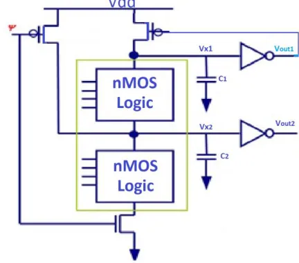
[image:3.612.356.523.393.566.2]During precharge phase whatever charge is present at output capacitor is distributed among junction capacitors of devices in evaluation phase. This effect leads in low output voltage which can be considered as low logic. Consider 3 input NAND gate shown in figure 6 to understand the charge sharing effect.
Fig 6: 3-input NAND gate using Domino Logic
Case1: when a=b=c=1 then output voltage during precharge mode will be VDD*CL. During Evaluation mode output voltage will be zero.
International Journal of Emerging Technology and Advanced Engineering
Website: www.ijetae.com (ISSN 2250-2459, ISO 9001:2008 Certified Journal, Volume 7, Issue 12, December 2017)
[image:4.612.360.565.136.310.2]274
Fig 7: Equivalent Diagram of the NAND gate logic when
input is 110
When input =110 a, b are ON switches and ‗c‘ is off. In the above case whatever charge stored in CL is now distributed among C1 and C2 (C3 is open switch) then
CL*VDD= VA (CL+ C1+ C2)
Where VA is node voltage obtained.
The above equation represents law of conservation i.e. charge is distributed but not lost. From above equation
VA = CL* VDD/ (CL+ C1+C2)
Charge in CL is distributed to C1 and C2. Let C1 = C2 =0.5 CL then
VA = CL* VDD/ (CL+0.5 CL +0.5 CL)
VA = VDD/2
From the above equation it‘s clear that instead of VDD the output voltage has reduced to VDD/2. During precharge phase because of parasitic capacitances present at internal node the charge present on CL is distributed among junction capacitances leading to reduction of output voltage by half.
The method adopted to overcome this problem is - A weak PMOS is added as pull up transistor as shown in fig 8. (A weak PMOS is always grounded so that it is always ON). Its resistance is high and allows very less current supply to the load capacitance and as a consequence it will replenish the charge that is lost.
Fig 8: Domino Logic with Precharge Transistor (Weak PMOS)
[image:4.612.92.247.142.248.2]During evaluation mode output voltage is not exactly equal to VDD there will be a small voltage drop due to weal PMOS. However the output discharges through the strong NMOS network. This strong NMOS network pulled down the output voltage to zero. When output is zero weak PMOS is ON which leads to static power dissipation. So to avoid this extra inverter is added at weak PMOS gate terminal as shown in fig 9.
Fig 9: Modified Domino logic to prevent Charge sharing
[image:4.612.336.552.434.624.2]International Journal of Emerging Technology and Advanced Engineering
Website: www.ijetae.com (ISSN 2250-2459, ISO 9001:2008 Certified Journal, Volume 7, Issue 12, December 2017)
275
to the weal PMOS =0it is turned ON and helps to drive to VDD.
V. MITIGATIONTECHNIQUESTOAVOIDSEE
The effects caused by radiations are not avoidable but TID and SEE can be reduced to acceptable levels with different CMOS approaches to be considered during designing and through other mitigation techniques [8]
1. Hardening by technology: Where fabrication is done by specific technology process.
2. Hardening by design: To make a device immune to SEE, the logic structures are modified.
3. Hardening by system: Duplication of logic or modifications in the software is done.
Hardening by technology: Based on technology process when charged particle strikes the silicon part, it affects the device in different ways. Standard CMOS technology is not robust to radiation, it doesn‘t eliminate SEE. EPI bulk CMOS is immune to SEL but not SEU. Practically Silicon on Insulator (SOI) eliminates the problem of SEE. In SOI a thin layer of silicon is placed on top of insulator during manufacturing process [8-9]. The transistors are placed on the top of this thin layer which reduces the capacitance thus making the device latch-up free [11][ 14]. This thin layer of silicon helps to protect the device from charged particles thus reducing SEU effect.
Hardening by design: In this design level approach standard CMOS design is used. Different applications circuits will have different solution using CMOS standards [2-3]. The following are the design level approaches:
Cyclic redundancy code (CRC): this method is used for end-to-end checking for packet processing design. This design ensures that if any modifications caused in data during transmission due to SEE, the data will be captured and re-transmission of that packet is requested.
Triple modular redundancy (TMR): It is triplication of design with voter element; it ensures that if an SEU changes the state of one machine then also it doesn‘t affect the design [11].
Hardening by system: In this design, modification in software or duplicating the logic is used. Error Detection and Correction Solutions (EDAC) is used to detect or correct the data which is flipped due to SEU effect [9][ 11].
Layout Techniques
There are some layout techniques which can be adopted during designing process which reduces the effect of SEE on the device.
Edgeless Transistors: These are MOS transistors with annular gate shape. Such type of geometry helps in reducing leakage current and eliminates bird‘s beak leakage effect thus reducing SEE effect [3, 11].
Guard rings: In this method NMOS should guarded by a p+ ring and PMOS with n+ ring. Which reduces the inter device leakage and eliminates latch up problem [12][ 14].
Multi finger Layout: In this technique the single transistor shown in fig 10 (a) is spited into two i.e. multi finger technique two transistors shares same source (drain is spitted) as shown in fig (b). This technique reduces the gate resistance and layout is more compact.
(a)
(b)
Fig 10: (a) Normal transistor Layout (b) Transistor Layout with Spitted Drain
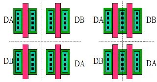
[image:5.612.364.524.582.666.2]Common Centroid Layout: Place the transistor as close as possible to reduce the chip mismatch as shown in fig 11. In this technique a common centroid is created which makes them immune from cross chip gradients and achieve best matching performance [19].
International Journal of Emerging Technology and Advanced Engineering
Website: www.ijetae.com (ISSN 2250-2459, ISO 9001:2008 Certified Journal, Volume 7, Issue 12, December 2017)
276
VI. CONCLUSION
Digital circuits designed for space applications must be robust and radiation tolerant. The charge particles present in radiation environment leads to Destructive and Nondestructive effects. This paper summarizes the behavior of Digital circuits under radiation environment. The Undesired effect of particle strike on digital circuits like TID, SOFT &HARD errors and circuit characteristics under such situations are briefly discussed. Different mitigation techniques used at different level of design and different layout techniques which can be adopted in order to make design radiation tolerant are discussed.
References
[1] E. Dod, M. R. Shaneyfelt, J. R. Schwank, and J. A. Felix, ―Current
and Future Challenges in Radiation Effects on CMOS Electronics‖ IEEE Transactions August vol. 57 no 4 2010
[2] Rakesh Trivedi , ―A SURVEY OF RADIATION HARDENING BY
DESIGN (RHBD) TECHNIQUES FOR ELECTRONIC SYSTEMS FOR SPACE APPLICATION‖ , (IJECET)Volume 7, Issue 1, Jan-Feb 2016, pp. 75-86, Article ID: IJECET_07_01_008
[3] Praveen Rathore and Sangeeta Nakhate, ―Development of Radiation
Hardened by Design (RHBD) ofNAND Gate to Mitigate the Effects of Single Event Transients (SET)‖ , 1st IEEE International Conference on Power Electronics. Intelligent Control and Energy Systems (ICPEICES-2016)
[4] Eric Cameron, Lowell Miles,Sterling Whitaker,Sterling Whitaker
―Heavy Ion Test Results of RHBD Standard Cells and Memory in a 110nm Bulk CMOS Process‖ 978-1-4799-1622-1/14/$31.00 ©2014 IEEE
[5] N. N. Mahatme, N. J. Gaspard, S. Jagannathan, T. D. Loveless, I.
Chatterjee, B. L. Bhuva, L. W. Massengill, and R. D. Schrimp ―Experimental Estimation of the Window of Vulnerability for Logic Circuits‖ ,IEEE TRANSACTIONS ON NUCLEAR SCIENCE, VOL. 60, NO. 4, AUGUST 2013
[6] Oluwole A. Amusan, Lloyd W. Massengill, Bharat L. Bhuva,
Sandeepan DasGupta, Arthur F. Witulski, ―Design Techniques to
Reduce SET Pulse Widths in
Deep-Submicron Combinational Logic‖, IEEE TRANSACTIONS ON NUCLEAR SCIENCE, VOL. 54, NO. 6, DECEMBER 2007
[7] Robert Baumann (Texas Instruments), "Single-Event Effects
inAdvancedCMOS Technology," IEEE NSREC Short Course, Short Course, Sect. II, pp 1-59, July 2005.
[8] D.G. Mavis and P.H. Eaton, ―Soft Error Rate Mitigation
TechniquesforModern Microcircuits,‖ IEEE IRPS, pp 216-225, April2002.
[9] Pitsini Mongkolkachit and Bharat Bhuva, “Design Technique for
Mitigation of Alpha-Particle-Induced Single-Event Transients in Combinational Logic‖, IEEE TRANSACTIONS ON DEVICE AND MATERIALS RELIABILITY, VOL. 3, NO. 3, SEPTEMBER 2003 [10] Sana Rezgui, John McCollum, J.J. Wangand Raymond Won
―Design and Layout Effects on SET Propagation in 90-nm ASIC and FPGA Test Structures‖ , TNS-x-2009.x
[11] Rajesh Garg and Sunil P.Khatri ―Analysis and Design of Resilient VLSI Circuits- Mitigating Soft Errors and Process Variations‖ Springer Publications.
[12] Christopher Saint and Judy Saint ―IC Layout Basics – A practical Guide‖ McGraw-Hill Publications.
[13] Ken LaBel ,Lew Cohn , ―Radiation Testing and Evaluation Issues for Modern Integrated Circuits‖, NASA/GSFC
[14] W. Dawes, Jr. and G. Gerbenwick, ―Prevention of CMOS Latch-upiNMOS Integrated Circuits,‖IEEE
[15] Sammy Kayali, ―Space Radiation Effects on Microelectronics‖ [16] B.R. Hancock, G.A. Soli ―Total Dose Testing of a CMOS Charged
Particle Spectrometer , IEEE TRANSACTIONS ON NUCLEAR SCIENCE, VOL. 44, NO. 6
[17] ―Radiation Design Considerations Using CMOS Logic‖by Texas instrument.
[18] K. LaBel, et al., ―Radiation Effects Characterization and Test MethodsofSingle-Chip and Multi-Chip Stacked 16 Mbit DRAMs,‖ IEEE Trans. Nucl. Sci., Vol. 43, No. 6, pp 2974
[19] Andrew T. Kelly, Patrick R. Fleming, W. Timothy Holman, Arthur F. Witulski, Bharat L. Bhuva, and Lloyd W. Massengil, ―Differential Analog Layout for Improved ASET Tolerance‖ , IEEE TRANSACTIONS ON NUCLEAR SCIENCE, VOL. 54, NO. 6, DECEMBER 2007