Safe Operating Condition and Lifetime
Estimation in p-MOSFET Device Due To
Negative Bias Temperature Instability
H. Hussin
a,band N.Soin
ba Faculty of Electrical Engineering, Universiti Teknologi MARA, Shah Alam, Malaysia b Department of Electrical Engineering, University of Malaya, Kuala Lumpur, Malaysia
Abstract - Negative Bias Temperature Instability is a serious reliability concerns for modern p-MOSFETs with Effective Oxide Thickness less than 2nm. This reliability problem can severely affect the device performance and limit the lifetime of the device. This paper is focusing on the safe operating condition and lifetime estimation of the p-MOSFET device with regard to NBTI effects. To explore the variation of safe operating condition and lifetime estimation, p-MOSFET having EOT 1nm was systematically simulated by varying the hydrogen species, measurement delay, stress temperature and stress gate voltage. The hydrogen species is varied based on molecular and atomic hydrogen. The measurement delay is simulated based on the measurement delay as found in literature. The stress temperature is varied from 800C to 1000C and the stress gate voltage is varied from -0.5V to -1V. The simulation result shows that the safe operating voltage for molecular hydrogen and atomic hydrogen is almost the same but the device lifetime estimation for molecular hydrogen is less than atomic hydrogen. For higher measurement delay, the lifetime estimation is higher compare to no delay while the safe operating voltage estimated for 5 years lifetime shows no significant different. The lifetime estimation for variation of temperature shows that the higher stress temperature contributes to more reduction in the device lifetime. The safe operating voltage condition is decreases as the temperature increases. Meanwhile, for the simulated stress voltage, the lifetime estimation of the device is increases as the absolute value of the stress voltage decreases.
Keywords: Negative Bias Temperature Instability, device lifetime estimation, safe operating condition, p-MOSFETs, molecular hydrogen species, atomic hydrogen species, R-D model
I.INTRODUCTION
Negative Bias Temperature Instability in p-MOSFET devices is an important reliability concern for advanced technology node. The performance of the devices is degraded due to this problem are threshold voltage, linear drain current and transconductance. This problem occurs when p-MOSFET is biased negatively at elevated temperature which contributes to the creation of interface traps and oxide
charges. This mechanism is clearly explained by R-D model. R-D model explains that interface trap concentrations, Nit are generated at Si02/Si interface by a reaction process. During this process, hydrogen is released and subsequently diffuses from the interface into the oxide by a diffusion process. The role of interface trap, Nit is very important in determining the degradation mechanism in transistor performance and the generation rate of Nit is expressed in (1) [1]:
(1)
where NO is initial number of Si-H bonds, NIT is interface traps concentration, and NOH is the number of atomic hydrogen at Si-SiO2 interface. Kf and kr are Si-H bond breaking and recovery rates respectively. As the Si-H bond broken, atomic hydrogen will released and diffuse away from the interface and will recombine with another atomic hydrogen to produce molecular hydrogen. Analysis by [2] is focusing on the possible diffusing species that contribute to NBTI degradation. Simulation based on different model based on the analysis as shown in (2) and (3) give different slope for different processes. If atomic hydrogen model is used, the time dependent is t0.25 while for molecular hydrogen, the time dependent is t0.165.
(2)
0.5 (3) A lot of research on various aspect of NBTI degradation has
been widely reported. Among of them, most research works were conducted to study the effect of stress temperature and gate voltage on the NBTI degradation by experimental [2-6], analytical [7-8] and simulation approach [9]. It is very important to carefully verify those parameters that significantly affect the NBTI degradation analysis. As NBTI is a reliability phenomenon, to estimate lifetime of the devices, it involves accelerated stress test where high stress gate voltage and temperature is applied to the devices.
as shown in Table 1 were previously developed to reduce the delay problem [4, 17-20].
TABLE I. MEASUREMENT TECHNIQUES
Measurement Technique Measurement Delay
Ultra Fast Stress Measure Stress 1 us
Conventional On The Fly 1 ms
Ultra Fast On The Fly 1 us
Fast Threshold Voltage 0.5 us
On The Fly Superimpose AC 1 s
Fast Pulse Measurement 100 ns
Lifetime estimation for device under NBTI degradation is varies associated with variation of stress parameter for accelerated test and various measurement techniques. With regard to that, a lot of effort has been taken to determine the lifetime of the device under study by using various approach [1, 14-15, 19, 21]. In this paper, the safe operating condition and lifetime estimation of p-MOSFET device will be studied by simulation using Modelling Interface-defect Generation (MIG) [22]. The effect of NBTI degradation on threshold voltage shift and interface trap concentration is analysed based on the simulation result.
II. SIMULATION CONDITIONS
The device used in this simulation is p-MOSFET with EOT 1nm since NBTI degradation is shown to be important reliability concern for technology nodes with EOT less than 2nm [1-2, 23]. The substrate doping level n-type silicon is fixed to 3e-17cm-3 and gate doping level is p+ poly silicon type is fixed at 1e20cm-3 for degenerate semiconductor. The forward dissociation model used in this simulation is based on model developed by [1]. This forward dissociation model explains NBTI degradation is field oxide dependent as shown in (4).
Kf = A EC exp(B Eox) (4) where EC is Semiconductor surface electric field due to mobile carriers and Eox is Oxide electric field. Another model employed in this simulation is Arrhenius model which is explained by [1] that NBTI degradation is temperature dependent. The activation energy, EA used in this simulation is 0.5 eV. For the lifetime prediction analysis, the change of maximum threshold voltage shift allowed is fixed to 60mV where estimation of lifetime is specified at five years. This five years lifetime is equivalent to ten years lifetime in CMOS operating condition which assuming 50% activity of p-MOSFET transistors [21]. In this analysis, the lifetime of the device is estimated at stress and safe conditions. To study the variation of prediction safe operating condition with respect to five years lifetime projection, the simulation is conducted in systematic approach where four different conditions are varied as shown in Table II.
TABLE II. SIMULATION CONDITION
Simulation Condition
Diffusing Species
Measurement
Delay Temperature Voltage
Diffusing
Species H, H2 0s 1000C 1.25V
Measurement
Delay H2
2s, 1ms, 1us
and 0s 1000C 1.25V
Stress
Temperature H2 0s
800C, 900C,
1000C 1.25V
Stress
Voltage H2 0s 1000C
1V, 0.75V,
0.5V
III. RESULT AND DISCUSSION
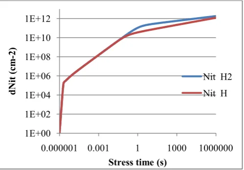
[image:2.595.300.550.344.518.2]A. Lifetime Dependency on Diffusing Hydrogen Species
Figure 1 shows interface trap concentration for molecular hydrogen, H2 and atomic hydrogen species. The interface trap concentration is plotted from the beginning of the stress to the end of stress time. It is observed that the interface trap concentration follow the R-D model. After initial phase, there is variation in the interface trap concentration which based on the type of hydrogen species.
Figure 1. Nit for Molecular Hydrogen Species and Atomic Hydrogen Species at early stress time
Figure 2 shows the variation in interface trap concentration where the graph is plotted at stress time 100s as extracted from Fig. 1. The interface trap concentration is follow the power law time dependence model (n ≈ 0.25 for H2 and n ≈
0.16 for H). 1E+00 1E+02 1E+04 1E+06 1E+08 1E+10 1E+12
0.000001 0.001 1 1000 1000000
dNit
(
cm
-2
)
Stress time (s)
Figure 2. Nit for Molecular Hydrogen Species and Atomic Hydrogen Species after 100 s stress time
Figure 3 shows threshold voltage shift for measurement time plotted at 10s to 10000s. Observed from the graph is the threshold voltage shift for molecular hydrogen follow power law time dependence where the slope is 0.171 while slope for atomic hydrogen is 0.251.
Figure 3. Vth shift for Molecular Hydrogen Species and Atomic Hydrogen Species
Table III shows safe stress condition for five years lifetime for different hydrogen species. Different hydrogen species lead to a slightly different in estimation of safe stress condition in five years lifetime. But the lifetime estimation at stress condition is significantly different for different hydrogen species. For molecular hydrogen, at stress voltage 1.25V, the estimated lifetime is 112931s while for atomic hydrogen with same stress bias gives lifetime estimation in longer time which is 1191700s.
TABLE III. SAFE OPERATING CONDITION AND LIFETIME ESTIMATION FOR DIFFERENT HYDROGEN SPECIES
Hydrogen Species Voltage (V) Lifetime (s)
H2 1.25 112931
0.684274 1.58E+08
B. Lifetime Dependency on Measurement Technique
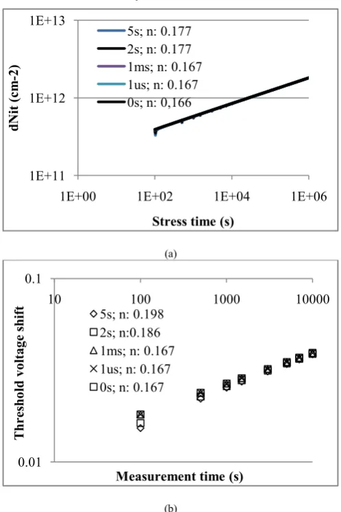
Figure 4 (a) and 4 (b) show interface trap concentration and threshold voltage shift as a function of stress time for different measurement delay respectively. These measurement delays correspond to different measurement technique as in literature. Different measurement delay contribute to slightly different time exponent, n. Note that the hydrogen species in this simulation is molecular hydrogen, H2 where time exponent, n ≈ 0.166. As measurement delay increases, the time exponent also increases. Similar to interface trap concentration, threshold voltage shift exhibits slightly different time exponent for each delay and increase as the measurement delay increased.
(a)
(b)
[image:3.595.35.282.326.490.2]Figure 4. NBTI degradation effects for molecular hydrogen species for different delay (a) Nit (b) Vth shift
Table IV shows safe stress condition for five years lifetime for different measurement delay. Different measurement delay lead to a slightly different in estimation of safe stress condition in five years lifetime. For five years lifetime, safe stress condition for measurement delay 2s, 1ms, 1us and 0s are 0.532695V, 0.684426V, 0.684274V and 0.684274V 1E+11
1E+12 1E+13
100 1000 10000 100000 1000000
dNit
(
cm
-2
)
Stress time (s)
H2; n:0.166 H; n:0.249
0.001 0.01 0.1 1
1 10 100 1000 10000
Thresho
ld Vo
lta
ge
shift
Measurement time (s)
H2; n:0.171 H; n:0.251
1E+11 1E+12 1E+13
1E+00 1E+02 1E+04 1E+06
dNit
(
cm
-2
)
Stress time (s)
5s; n: 0.177 2s; n: 0.177 1ms; n: 0.167 1us; n: 0.167 0s; n: 0,166
0.01 0.1
10 100 1000 10000
T
h
res
h
ol
d
vol
tage
sh
if
t
Measurement time (s)
5s; n: 0.198 2s; n:0.186 1ms; n: 0.167 1us; n: 0.167 0s; n: 0.167 H2
[image:3.595.52.264.659.745.2]to error in lifetime estimation. If the measurement delay is larger than 1ms, then it will contribute to error in lifetime estimation. The lifetime estimated is larger than the lifetime for measurement with no delay.
TABLE IV. SAFE OPERATING CONDITION AND LIFETIME ESTIMATION
FOR MEASUREMENT DELAY
Delay Voltage Lifetime
2s 1.25 63519.9
0.532695 1.58E+08
0.001s 1.25 113690
0.684426 1.58E+08
1e-06s 1.25 112931
0.684274 1.58E+08
0s 1.25 112931
0.684274 1.58E+08
C. Lifetime Dependency on Temperature
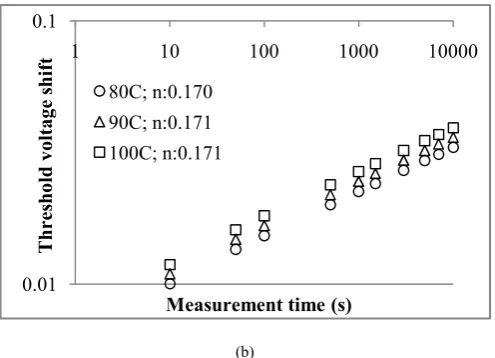
Figure 5 (a) and (b) shows interface trap concentration and threshold voltage shift as a function of stress time for different stress temperature. The temperature is varied from 800C to 1000C. From the simulation result, observed from Figure 5 (a), the time exponent is similar for each of the simulated temperature. This shows that the interface trap concentration is temperature independent for this range of temperature. Observed from the graph, the interface trap concentration is increases as the temperature increases. For Figure 5 (b), the threshold voltage shift slightly increases as the temperature increases. The interface trap concentration and threshold voltage shift follow power law where n ≈ 0.17 which reflect the hydrogen species used in this simulation is molecular hydrogen.
(a)
(b)
[image:4.595.76.241.162.305.2]Figure 5. NBTI degradation effects for molecular hydrogen species for different stress temperature (a) Nit (b) Vth shift
[image:4.595.76.242.164.305.2]Table V shows safe stress condition for five years lifetime for different stress temperature. As can be seen, the safe stress voltage condition is decreases as the temperature increases for five years lifetime estimation. The safe stress voltage condition is 0.759974, 0.721202 and 0.684274 for stress temperature 800C, 900C and 1000C respectively. The lifetime estimation for simulated stress voltage at 1.25V is different for different temperature which is decreases as temperature increases. For stress temperature 800C, 900C and 1000C, the lifetime is 316979s, 187260s and 112931s respectively.
TABLE V. SAFE OPERATING CONDITION AND LIFETIME ESTIMATION
FOR DIFFERENT STRESS TEMPERATURE
Temperature Voltage Lifetime
80C 1.25 316979
0.759974 1.58E+08
90C 1.25 187260
0.721202 1.58E+08
100C 1.25 112931
0.684274 1.58E+08
D. Lifetime Dependency on Gate Stress Voltage
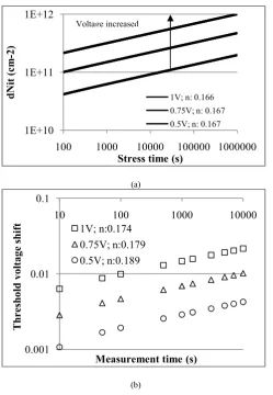
Figure 6 (a) and (b) shows interface trap concentration and threshold voltage shift as a function of stress time for different stress gate voltage. The interface trap concentration and threshold voltage shift is increases as the stress gate voltage increases. The degradation behaviours follow power law where time exponent for both is n ≈ 0.17 which again reflects the simulated hydrogen species is molecular hydrogen. The time exponent for both degradations is increases as the stress voltage decreases. Observed from threshold voltage shift graph, the time exponent is slightly higher than 0.17 at smaller stress voltage.
1E+11 1E+12 1E+13
90 9000 900000
dNit
(
cm
-2
)
Stress time (s)
80C; n: 0.166 90C; n: 0.166 100C; n: 0.166
0.01 0.1
1 10 100 1000 10000
T
h
res
h
ol
d
vol
tage
sh
if
t
Measurement time (s)
80C; n:0.170 90C; n:0.171 100C; n:0.171
[image:4.595.300.506.425.552.2] [image:4.595.34.286.496.665.2](a)
[image:5.595.35.285.81.442.2](b)
Figure 6. NBTI degradation effects for molecular hydrogen species for different stress voltage (a) Nit (b) Vth shift
Table VI shows safe stress condition for five years lifetime for different stress gate voltage. The lifetime for three level of stress voltage is simulated which at 1V, 0.75V and 0.5V. The lifetime for each of the simulated stress voltages are 3211540s, 1.73e08s and 9.64e08s respectively. For 0.75V and 0.5V the lifetime is higher than five years lifetime projection which can be said that the voltages are above the safe operating voltage condition.
TABLE VI. SAFE OPERATING CONDITION AND LIFETIME ESTIMATION FOR DIFFERENT STRESS GATE VOLTAGE
Voltage Lifetime
1 3211540
0.702713 1.58E+08
0.75 1.73E+08
0.756802 1.58E+08
0.5 9.64E+09
0.802776 1.58E+08
IV. CONCLUSION
estimation for the device is studied based on a various stress condition. The safe operating condition is varied depending on the type of hydrogen species. It is also shown that safe operating condition for different measurement delay is not significantly varied. For different stress temperature the safe operating condition almost similar while for different stress voltage the safe operating condition is less than simulated value. Lifetime estimation is varied depending on the type of hydrogen species, measurement delay, applied stress temperature and gate voltage.
ACKNOWLEDGEMENT
The authors acknowledge the financial support from Universiti Teknologi MARA and Ministry of Higher Education (Fundamental Research Grant Scheme, FRGS) for the implementation of this research work. The main author is a student registered with University of Malaya. Proof read made by Wan Fazlida Hanim Abdullah from Universiti Teknologi MARA is gratefully acknowledged.
REFERENCES
[1] M. A. Alam and S. Mahapatra, "A comprehensive model of PMOS NBTI degradation," Microelectronics Reliability, vol. 45, pp. 71-81, 2005.
[2] S. Chakravarthi, et al., "A comprehensive framework for predictive modeling of negative bias temperature instability," in 2004 IEEE International Reliability
Physics Symposium Proceedings, 2004, pp. 273-282.
[3] V. Huard, et al., "A thorough investigation of MOSFETs NBTI degradation," Microelectronics Reliability, vol. 45, pp. 83-98, 2005.
[4] E. N. Kumar, et al., "Material Dependence of NBTI Physical Mechanism in Silicon Oxynitride (SiON) p-MOSFETs: A Comprehensive Study by Ultra-Fast On-The-Fly (UF-OTF) Technique," in Electron Devices
Meeting, 2007. IEDM 2007. IEEE International, 2007,
pp. 809-812.
[5] S. Mahapatra, et al., "Investigation and modeling of interface and bulk trap generation during negative bias temperature instability of p-MOSFETs," IEEE
Transactions on Electron Devices, vol. 51, pp.
1371-1379, 2004.
[6] L. Yuhao, et al., "Mechanism and Modeling of PMOS NBTI Degradation with Drain Bias," in 45th Annual IEEE International Reliability Physics Symposium, 2007, 2007, pp. 264-267.
[7] L. Hong, et al., "Modeling of PMOS NBTI Effect Considering Temperature Variation," in 8th International Symposium on Quality Electronic Design, 2007. ISQED '07. , 2007, pp. 139-144.
[8] T. P. C. J. B Yang, S. S. Tan and L. Chen, "Analytical reaction-diffusion model and the modeling of nitrogen-enhanced negative bias temperature instability," Applied Physics Letters, vol. 88, 2006.
[9] S. F. W. M. Hatta, et al., "NBTI degradation effect on 1E+10
1E+11 1E+12
100 1000 10000 100000 1000000
dNit
(
cm
-2
)
Stress time (s)
1V; n: 0.166 0.75V; n: 0.167 0.5V; n: 0.167
0.001 0.01 0.1
10 100 1000 10000
T
h
res
h
ol
d
vol
tage
sh
if
t
Measurement time (s)
[10] M. A. Alam, "A critical examination of the mechanics of dynamic NBTI for PMOSFETs," pp. 14.4.1-14.4.4. [11] J. Lei and X. Mingzhen, "Investigation of NBTI
recovery induced by conventional measurements for pMOSFETs with ultra-thin SiON gate dielectrics," in IEEE International Integrated Reliability Workshop Final Report, 2007. IRW 2007., 2007, pp. 38-42. [12] C. Schlunder, et al., "On the impact of the NBTI
recovery phenomenon on lifetime prediction of modern p-MOSFETs," in Integrated Reliability Workshop Final Report, 2006 IEEE International, 2006, pp. 1-4. [13] S. Rangan, et al., "Universal recovery behavior of
negative bias temperature instability [PMOSFETs]," in Electron Devices Meeting, 2003. IEDM '03 Technical Digest. IEEE International, 2003, pp. 14.3.1-14.3.4. [14] S. Mahapatra and M. A. Alam, "Defect Generation in
p-MOSFETs Under Negative-Bias Stress: An Experimental Perspective," Device and Materials
Reliability, IEEE Transactions on, vol. 8, pp. 35-46,
2008.
[15] H. Reisinger, et al., "A Study of NBTI and Short-Term Threshold Hysteresis of Thin Nitrided and Thick Non-Nitrided Oxides," Device and Materials Reliability, IEEE Transactions on, vol. 9, pp. 106-114, 2009. [16] D. K. Schroder, "Negative bias temperature instability:
What do we understand?," Microelectronics Reliability, vol. 47, pp. 841-852, 2007.
[17] M. Denais, et al., "On-the-fly characterization of NBTI in ultra-thin gate oxide PMOSFET's," in Electron Devices Meeting, 2004. IEDM Technical Digest. IEEE International, 2004, pp. 109-112.
[18] W. J. Liu, et al., "On-The-Fly Interface Trap Measurement and Its Impact on the Understanding of NBTI Mechanism for p-MOSFETs with SiON Gate Dielectric," in Electron Devices Meeting, 2007. IEDM 2007. IEEE International, 2007, pp. 813-816.
[19] V. D. Maheta, et al., "Development of an Ultrafast On-the-Fly Technique to Study NBTI in Plasma and Thermal Oxynitride p-MOSFETs," IEEE Transactions on Electron Devices, vol. 55, pp. 2614-2622, 2008. [20] L. Ming-Fu, et al., "Understand NBTI Mechanism by
Developing Novel Measurement Techniques," IEEE Transactions on Device and Materials Reliability, vol. 8, pp. 62-71, 2008.
[21] A. E. Islam, et al., "Optimization of Gate Leakage and NBTI for Plasma-Nitrided Gate Oxides by Numerical and Analytical Models," Electron Devices, IEEE Transactions on, vol. 55, pp. 1143-1152, 2008.
[22] A. E. Islam, et al., "Modeling Interface-defect Generation (MIG)," ed, 2006.