A Universal Amplifier Module (UAM) in 0.18 µm CMOS
(CMOSP18/TSMC) Technology With Some Applications in Analog
Signal Processing
Md. Aminul Haque Talukder
A Thesis
in
The Department
of
Electrical and Computer Engineering
Presented in Partial Fulfillment of the Requirements
for the Degree of Master of Applied Science at
Concordia University
Montreal, Quebec, Canada
September 2011
CONCORDIA UNIVERSITY SCHOOL OF GRADUATE STUDIES
This is to certify that the thesis prepared
By: Md. Aminul Haque Talukder
Entitled: “A Universal Amplifier Module (UAM) in 0.18 µm CMOS (CMOSP18/TSMC) Technology with some Applications in Analog Signal Processing”
and submitted in partial fulfillment of the requirements for the degree of
Master of Applied Science
Complies with the regulations of this University and meets the accepted standards with respect to originality and quality.
Signed by the final examining committee:
________________________________________________ Chair Dr. A. Aghdam
________________________________________________ Examiner, External
Dr. C. Assi (CIISE) To the Program
________________________________________________ Examiner Dr. G. Cowan ________________________________________________ Supervisor Dr. R. Raut Approved by: ___________________________________________ Dr. W. E. Lynch, Chair
Department of Electrical and Computer Engineering
____________20_____ ___________________________________
Dr. Robin A. L. Drew
Dean, Faculty of Engineering and Computer Science
iii
ABSTRACT
A Universal Amplifier Module (UAM) in 0.18 µm CMOS
(CMOSP18/TSMC) Technology With Some Applications in Analog
Signal Processing
Md. A. H. TalukderThe amplifiers such as operational amplifier, operational transconductance amplifier, operational transresistance amplifier, current conveyor etc. are the basic building blocks in analog circuits and systems. These important basic amplifiers find wide spread applications in the integration of several electronic systems. However, different analog devices are preferred for different systems. It is difficult to use a single type of device to cater for the needs of different systems with diverse input output impedance environments.
In this thesis work, a Universal Amplifier Module (UAM) is designed and implemented in a modern 0.18µm CMOS (CMOSP18/TSMC) technology and its applications toward realization of second order voltage and current – mode filters are reported. Concepts of network transposition and nullor equivalent of ideal active devices are utilized to realize both voltage and current – mode filters using the same UAM module which is able to provide all the voltage and current mode operations (such as, OP-AMP with VCVS, OTA with VCCS, OTRA with CCVS, and CCCS).
iv
ACKNOWLEDGEMENTS
The research was supported by a grant awarded to Dr. Rabin Raut by the Natural Science and Engineering Research Council (NSERC), Canada.
I am grateful for all the supports and encouragements I have received from my supervisor Dr. R. Raut. His enthusiasm for my work and willingness to always offer his help no matter how busy he is, either on campus or on leave, is greatly appreciated. I would like to give him thanks for suggesting various ideas and insightful comments at different stages of my research.
Thanks to all the members of the Concordia ECE VLSI Lab, especially Mr. Tadeusz Obuchowicz for his helps and suggestions on various technical issues.
Special thanks to Dr. A. Aghdam, Dr. G. Cowan, Dr. C. Assi and Dr. R. Raut for their constructive criticisms regarding the work during the oral presentation.
We remain grateful to Canadian Microelectronics Corporation (CMC) Inc., community for allowing us to have access to the CMOSP18/TSMC technology and various CAD tools related to VLSI design and implementation.
v
DEDICATIONS
To My Beloved Parents and brothers for their love, affection,
encouragement and inspiration in every step of my life.
vi
TABLE OF CONTENTS
LIST OF FIGURES ... x
LIST OF TABLES ... xiii
LIST OF SYMBOLS AND ABBREVIATIONS ... xiv
CHAPTER 1 ... 1
INTRODUCTION ... 1
1.1 Basic electronic amplifiers... 1
1.1.1 VCVS ... 2
1.1.2 VCCS ... 3
1.1.3 CCVS ... 4
1.1.4 CCCS ... 5
1.2 Practical electronic amplifiers ... 7
1.2.1 Operational Amplifier (OP-AMP) ... 7
1.2.2 Operational transconductance amplifier (OTA) ... 8
1.2.3 Operational Transresistance amplifier (OTRA) ... 10
1.2.4 Current Conveyor (CC) ... 11
1.3 Motivation ... 13
1.4 Organization of thesis ... 14
CHAPTER 2 ... 15
ANALYSIS AND DESIGN OF THE UNIVERSAL AMPLIFIER MODULE (UAM) ... 15
2.1 Introduction ... 15
2.2 Bias sources... 16
2.3 Differential input stages... 17
2.4 Intermediate stages ... 19
2.5 Frequency compensation ... 21
2.6 Voltage buffer stage ... 22
2.7 Current buffer stage ... 23
2.8 The Universal Amplifier Module (UAM) ... 26
2.9 Voltage and current – mode operations of the UAM ... 27
2.9.1 Implementation of VCVS using the UAM ... 27
vii
2.9.3 Implementation of VCCS using the UAM ... 31
2.9.4 Implementation of CCCS using the UAM ... 34
2.10 Summary ... 37
CHAPTER 3 ... 38
CHARACTERIZATION OF THE UAM USING SIMULATIONS ... 38
3.1 Introduction ... 38
3.2 Complete Schematic of UAM ... 39
3.3 Dimensions of the transistors ... 40
3.4 Performance parameters measurements ... 41
3.4.1 Open loop frequency response ... 42
3.4.2 Phase margin and Gain margin ... 43
3.4.3 Input offset voltage... 44
3.4.4 Input common mode range (ICMR) ... 45
3.4.5 Output voltage swing ... 46
3.4.6 Output offset voltage ... 47
3.4.7 Slew rate measurement ... 48
3.4.8 Common mode rejection ratio (CMRR) ... 49
3.4.9 Power supply rejection ratio (PSRR) ... 51
3.5 Complete Layout of UAM ... 52
3.6 Performance parameters for VCCS, CCVS and CCCS ... 53
3.7 Common-Mode Feedback (CMFB) ... 54
3.8 Comparison between the UAM and reported work in the literature ... 57
3.8.1 Comparison between UAM (operating as OP-AMP) and reported work in literature ... 57
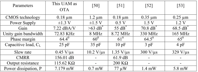
3.8.2 Comparison between the UAM (operating as OTA) and reported work in literature ... 58
3.8.3 Comparison between the UAM (operating as OTRA) and reported work in literature ... 58
3.8.4 Comparison between the UAM (operating as CCII) and reported work in literature ... 59
3.9 Post layout simulations ... 59
3.9.1 Layout of bias sources ... 59
3.9.2 Layout of input differential amplifier stages ... 61
3.9.3 Layout of intermediate stages ... 62
3.9.4 Layout of voltage buffer stage ... 64
3.9.5 Layout of current buffer stage ... 66
viii
CHAPTER 4 ... 68
APPLICATION CASES OF THE UAM ... 68
4.1 Introduction ... 68
4.2 Inverting amplifier implementation ... 68
4.3 Non-inverting amplifier implementation ... 70
4.4 Voltage follower (unity gain buffer) implementation ... 72
4.5 Ideal inverting integrator implementation ... 74
4.6 Lossy integrator implementation ... 76
4.7 Current conveyor (CCII) realization using UAM ... 78
4.8 Voltage-mode filter (VMF) implementation using three UAM ... 79
4.9 Transconductance filter (TCF) implementation using three UAM ... 83
4.10 Current-mode filter (CMF) implementation using three UAM ... 86
4.11 Transresistance filter (TRF) implementation using three UAM ... 90
4.12 Use of UAM as electronic sensors and actuators... 94
4.12.1 UAM for Micro Mechanical Sensors and Actuator Circuitry ... 95
4.12.2 Pressure Transducer to ADC Application using UAM ... 97
4.13 Summary ... 99
CHAPTER 5 ... 100
CONCLUSION AND FUTURE WORKS ... 100
5.1 Conclusion ... 100
5.2 Recommendations for Future Works ... 101
5.2.1 Optimization of the layout ... 101
5.2.2 Chip fabrication and test ... 102
5.2.3 UAM in other technologies ... 102
REFERENCES ... 103
APPENDIX – A ... 110
A.1 Ackerberg and Mossberg (A & M) biquadratic filters ... 110
APPENDIX – B ... 112
B.1 The Voltage-Mode A & M Filter... 112
APPENDIX – C ... 115
C.1 The Current-Mode A & M Filter ... 115
APPENDIX – D ... 117
ix
D.1.1 Open loop frequency response ... 117
D.1.2 Input common mode range (ICMR) ... 118
D.1.3 Input and output offset voltage ... 119
D.1.4 Output voltage swing ... 120
D.2 Simulation set-up for CCCS ... 121
D.2.1 Open loop frequency response ... 121
D.2.2 Input common mode range (ICMR) ... 123
D.2.3 Output voltage swing ... 124
D.3 Simulation set-up for VCCS ... 125
D.3.1 Open loop frequency response ... 125
D.3.2 Input and output offset voltage ... 126
APPENDIX – E ... 128
E.1 SPICE file for the NETLIST of the Universal Amplifier Module ... 128
APPENDIX – F ... 132
x
LIST
OF
FIGURES
Figure 1.1: Equivalent circuit of VCVS 2
Figure 1.2: Equivalent circuit of VCCS 3
Figure 1.3: Equivalent circuit of CCVS 4
Figure 1.4: Equivalent circuit of CCCS 6
Figure 1.5: Block diagram of an OP-AMP with different sub systems 7
Figure 1.6: Single ended output OTA 9
Figure 1.7: Differential output OTA 9
Figure 1.8: Circuit symbol of OTRA 10
Figure 1.9: Block diagram of a current conveyor (CC) 11
Figure 2.1: Block diagram of the Universal Amplifier Module (UAM) 16
Figure 2.2: Schematic diagram of the bias sources 16
Figure 2.3: (a) Schematic diagram of differential input stage (b) Small signal equivalent model of DA stage 18
Figure 2.4: Schematic diagram of the input stage of the UAM 19
Figure 2.5: (a) Schematic diagram of intermediate stages; (b) Small signal equivalent model 20 Figure 2.6: (a) Schematic diagram of the voltage buffer stage; (b) Small signal model of the voltage buffer 23 Figure 2.7: Schematic diagram of the current buffer stage of the UAM 24
Figure 2.8: Small signal equivalent model of the transconductor 25
Figure 2.9: Schematic diagram of the half circuit of the universal amplifier module (UAM) 26
Figure 2.10: Schematic diagram of the half circuit of VCVS implementation of the UAM 28
Figure 2.11: Small signal equivalent circuit of the UAM configured as VCVS 28
Figure 2.12 Schematic diagram of CCVS implementation of the UAM 29
Figure 2.13: Small signal equivalent circuit of CCVS configuration 30
Figure 2.14: Schematic diagram of VCCS implementation of the UAM 31
Figure 2.15: Small signal equivalent model of the half circuit of VCCS 32
Figure 2.16: Schematic diagram of CCCS implementation of the UAM 34
Figure 2.17: Small signal equivalent model of the half circuit of CCCS 35
Figure 3.1: Complete schematic diagram of the UAM in 0.18 µm CMOS (CMOSP18/TSMC) technology 39
Figure 3.2: Configuration for open loop frequency response 42
Figure 3.3: Magnitude and phase response of the VCVS 43
Figure 3.4: (a) Configuration for measuring input offset voltage (b) Simulated result of input offset voltage 44
Figure 3.5: Configuration for measuring input common mode range (ICMR) 45
Figure 3.6: Simulated ICMR characteristics 46
Figure 3.7: Measurement set-up for output voltage swing 46
Figure 3.8: Simulated output voltage swing 47
Figure 3.9: Configuration for measuring slew rate 48
Figure 3.10: Simulated result of slew rate measurement 49
Figure 3.11: Measurement set-up for CMRR 50
Figure 3.12: Simulated CMRR response 50
Figure 3.13: Configuration for measuring PSRR 51
Figure 3.14: Simulated result for PSRR frequency response 52
Figure 3.15: Complete layout of the UAM in 0.18 µm CMOS (CMOSP18/TSMC) technology 52
Figure 3.16: Differential Difference Amplifier CMFB circuit [38] 54
Figure 3.17: Complete diagram of the CMFB implementation with the UAM 56
Figure 3.18: Simulated output of the VCVS after using CMFB 56
Figure 3.19: (a) Layout of the bias sources; (b) test block of the bias source 60
xi
Figure 3.21: (a) Layout of the input differential stages; (b) Test block of the input DA stages 61
Figure 3.22: Simulated DC level and output AC signal of the input DA stages 61
Figure 3.23: (a) Layout of the intermediate stages; (b) Test block of the intermediate stages 62
Figure 3.24: Simulated output of the intermediate stage comprising transistors M13 & M15 63
Figure 3.25: Simulated output of the intermediate stage comprising transistors M17 & M23 64
Figure 3.26: (a) Layout of the voltage buffer stage; (b) Test block of the voltage buffer 65 Figure 3.27: Simulated output of the voltage buffer stage 65 Figure 3.28: (a) Layout of the current buffer stage; (b) Test block of the current buffer 66 Figure 3.29: Simulated output of the current buffer stage 66 Figure 4.1: Inverting amplifier implementation using the UAM 69 Figure 4.2: Output of the inverting amplifier for gain of -1 (Ri = 1 KΩ, Rf = 1 KΩ) 69 Figure 4.3: Output of the inverting amplifier for gain of -10 (Ri = 1 KΩ, Rf = 10 KΩ) 70 Figure 4.4: Non-inverting amplifier implementation using the UAM 71 Figure 4.5: Output of the non-inverting amplifier for gain of +5 (Ri = 1 KΩ, Rf = 4 KΩ) 71 Figure 4.6: Output of the non-inverting amplifier for gain of +10 (Ri = 1 KΩ, Rf = 9 KΩ) 72 Figure 4.7: Voltage follower implementation using UAM 73 Figure 4.8: Simulated output of the voltage follower 73 Figure 4.9: Ideal inverting integrator implementation using UAM 74 Figure 4.10: Magnitude response of the inverting integrator 75 Figure 4.11: Phase response of the inverting integrator 75 Figure 4.12: Lossy integrator implementation using UAM 76 Figure 4.13: Magnitude response of the lossy integrator 77 Figure 4.14: Phase response of the lossy integrator 77 Figure 4.15: CCII implementation using UAM 78 Figure 4.16: CCII simulation set-up 78 Figure 4.17: Simulated output of the CCII 79 Figure 4.18: Voltage-mode BPF implementation using UAM 81 Figure 4.19: Frequency response of the VMF for fp = 10 KHz 82 Figure 4.20: Frequency response of the VMF for fp = 1 MHz 83 Figure 4.21: Transconductance filter implementation using the UAM 84 Figure 4.22: Frequency response of the TCF for fp = 10 KHz 84 Figure 4.23: Frequency response of the TCF for fp = 10 MHz 85 Figure 4.24: Current-mode BPF implementation using UAM 87 Figure 4.25: Frequency response of the CMF for fp = 10 KHz 88 Figure 4.26: Frequency response of the CMF for fp = 10 MHz 89 Figure 4.27: Transresistance BPF implementation using UAM 90 Figure 4.28: Frequency response of the TRF for fp = 1 KHz 92 Figure 4.29: Frequency response of the TRF for fp = 100 KHz 93 Figure 4.30: Capacitive-coupled MEMS oscillator using the proposed UAM 95 Figure 4.31: OP-AMP circuit for the pressure transducer to ADC application 98 Figure A.1.1: Voltage-mode A & M biquadratic filter 111 Figure A.1.2: Current-mode A & M biquadratic filter 111 Figure D.1.1: Configuration for open loop frequency response of the CCVS 117
Figure D.1.2: Magnitude response of the CCVS 117
Figure D.1.3: Phase response of the CCVS 118
Figure D.1.4: Configuration for measuring input common mode range of the CCVS 118
Figure D.1.5: Simulated ICMR characteristics of the CCVS 119
Figure D.1.6: Configuration for measuring input offset of the CCVS 119
xii
Figure D.1.8: Measurement set-up for output voltage swing of the CCVS 120
Figure D.1.9: Simulated output voltage swing of the CCVS 121
Figure D.2.1: Configuration for open loop frequency response of the CCCS 121
Figure D.2.2: Frequency response of the CCCS 122
Figure D.2.3: Phase response of the CCCS 122
Figure D.2.4: Configuration for measuring input common mode range of the CCCS 123
Figure D.2.5: Simulated ICMR characteristics of the CCCS 123
Figure D.2.6: Measurement set-up for output swing of the CCCS with RL = 1 KΩ 124
Figure D.2.7: Simulated output swing of the CCCS 124
Figure D.3.1: Configuration for open loop frequency response of the VCCS 125
Figure D.3.2: Magnitude response of the VCCS 125
Figure D.3.3: Phase response of the VCCS 126
Figure D.3.4: Configuration for measuring input offset of the VCCS with RL = 1 KΩ 126
xiii
LIST
OF
TABLES
Table 3.1: Dimensions of the transistors used in UAM 41
Table 3.2: Table for performance parameters measurements 53
Table 3.3: Comparison between the UAM (operating as OP-AMP) and reported work in literature 57
Table 3.4: Comparison between the UAM (operating as OTA) and reported work in literature 58
Table 3.5: Comparison between the UAM (operating as OTRA) and reported work in literature 58
Table 3.6: Comparison between the UAM (operating as CCII) and reported work in literature 59
xiv
LIST
OF
SYMBOLS
AND
ABBREVIATIONS
C Capacitor
R Resistor
Qp Pole Quality Factor
ω Frequency in Radians
H(s) Frequency Domain Transfer Function
AC Alternating Current
V
th Threshold Voltage of the Transistor
IC Integrated Circuit
W Channel Width of the MOS Transistor
L Channel Length of the MOS Transistor
g
m AC Transconductance
VDD Positive Supply Voltage
VSS Negative Supply Voltage
CMOS Complementary Metal Oxide Semiconductor
PMOS Positive-channel Metal Oxide Semiconductor
NMOS Negative-channel Metal Oxide Semiconductor
MOSFET MOS Field Effect Transistor
VLSI Very Large Scale Integration
OP-AMP Operational Amplifier
OTA Operational Transconductance Amplifier
OTRA Operational Transresistance Amplifier
xv
VCVS Voltage Controlled Voltage Source
CCCS Current Controlled Current Source
CCVS Current Controlled Voltage Source
VCCS Voltage Controlled Current Source
CTF Current Transfer Function
VTF Voltage Transfer Function
VMF Voltage Mode Filter
CMF Current Mode Filter
TCF Transconductance Filter
TRF Transresistance Filter
BPF Band Pass Filter
ADC Analog-to-Digital Converter
VCT voltage to current transducer
CMFB Common Mode Feedback
1
CHAPTER
1
INTRODUCTION
1.1 Basic electronic amplifiers
An amplifier receives a signal at its input and delivers undistorted large signal at its output. Several applications of amplifiers include wireless communications and broadcasting, and in audio equipment of all kinds [1].
Amplifiers can be classified into four basic categories based on the magnitudes of the input and output impedances in comparison with the source and load impedances respectively. These are [1]:
►Voltage controlled voltage source amplifier (VCVS), ►Voltage controlled current source amplifier (VCCS), ►Current controlled voltage source amplifier (CCVS), and ►Current controlled current source amplifier (CCCS).
2 1.1.1 VCVS
It provides an output voltage proportional to the input voltage. The proportionality factor is independent of the magnitudes of source and load resistance. Figure 1.1 shows the Thevenin’s equivalent circuit of VCVS amplifier.
Figure 1.1: Equivalent circuit of VCVS
Here, Vs= source voltage, Vi= amplifier input voltage, Vo= output voltage, Rs= source resistance,
Ri= amplifier input resistance, Ro= amplifier output resistance, RL= external load resistance.
From the input circuit,
Vi = s i i R R R Vs Vi ≈ Vs (if Ri >> Rs) (1.1)
From the output circuit,
Vo = o R R R L L AvVi (1.2) Vo ≈ AvVi (if Ro << RL) Vo = AvVs (from equation (1.1))
3 From equation (1.2), Vo = o L L R R R AvVi Vo = AvVi (with RL = ) Av = i o V V
Hence Av represents the open-circuit voltage amplification, or voltage gain.
1.1.2 VCCS
It provides an output current proportional to the input voltage. The proportionality factor is independent of the magnitudes of source and load resistance. Figure 1.2 shows a VCCS amplifier, where Thevenin’s equivalent circuit is used at input side and Norton’s equivalent circuit is used at output side.
From the input circuit,
Vi = s i i R R R Vs Vi ≈ Vs (if Ri >> Rs) (1.3)
From the output circuit,
4 Io = o L o R R R GmVi (1.4) Io ≈ GmVi (if Ro >> RL) Io = GmVs (from equation (1.3))
Hence output current is proportional to input voltage.
An ideal VCCS amplifier must have infinite input resistance (i.e. Ri = ) and infinite output
resistance (i.e. Ro = ). From equation (1.4),
Io = o L o R R R AvVi Io = GmVi (with RL = 0) Gm = i o V I
Hence Gm represents the short-circuit trans-conductance gain.
1.1.3 CCVS
It provides an output voltage proportional to the input current. The proportionality factor is independent of the magnitudes of the source and load resistance. Figure 1.3 shows a CCVS amplifier where Norton’s equivalent circuit is used at input side and Thevenin’s equivalent circuit is used at output side.
5
From the input circuit,
Ii = s i s R R R Is Ii ≈ Is (if Ri << Rs) (1.5)
From the output circuit,
Vo = o L L R R R Rm Ii (1.6) Vo ≈ Rm Ii (if Ro << RL) Vo = Rm Is (from equation (1.5))
Hence, output voltage is proportional to input current.
An ideal CCVS amplifier must have zero input resistance (i.e. Ri =0) and zero output resistance
(i.e. Ro = 0). From equation (1.6), Vo = o L L R R R Rm Ii Vo = Rm Ii (with RL = ) Rm = i o I V
Hence Rm represents the open-circuit trans-resistance gain.
1.1.4 CCCS
It provides an output current proportional to the input current. The proportionality factor is independent of the magnitudes of the source and load resistance. Figure 1.4 shows a Norton’s equivalent circuit of a CCCS amplifier.
6
Figure 1.4: Equivalent circuit of CCCS
Here, Is= source current, Ii= amplifier input current, Io= IL= output or load current.
From the input circuit,
Ii = s i s R R R Is Ii ≈ Is (if Ri << Rs) (1.7)
From the output circuit,
Io = o L o R R R Ai Ii (1.8) Io ≈ Ai Ii (if Ro >> RL) Io = Ai Is (from equation (1.7))
Hence output current is proportional to input current.
An ideal current amplifier must have zero input resistance (i.e. Ri =0) and infinite output
resistance (i.e. Ro = ). From equation (1.8),
Io = o L o R R R Ai Ii Io = Ai Ii (with RL = 0)
7 Ai = i o I I
Hence Ai represents the short-circuit current gain.
1.2 Practical electronic amplifiers 1.2.1 Operational Amplifier (OP-AMP)
The operational amplifier (OP-AMP) is a fundamental building block in analog integrated circuit design [2-4]. It is a very useful and versatile building block which can provide many nearly ideal signal processing functions such as addition, subtraction, multiplication, integration and so on. Figure 1.5 shows the block diagram of important sub systems of an OP-AMP [5].
Differential Amplifier Intermediate Amplifiers Output Stage Frequency Compensation Biasing System V+ V- Vout
Figure 1.5: Block diagram of an OP-AMP with different sub systems
From the figure, V is the voltage at the non-inverting terminal and V is the voltage at the
inverting terminal. Ideally the OP-AMP amplifies only the difference in voltage between the two input terminals, which is called the differential input voltage. The output voltage of the OP-AMP is given by the equation,
OL out V V A
8
where, AOL is the called as open loop gain of the amplifier. The differential amplifier (DA) is an
essential part of OP-AMP. The DA may perform differential to single-ended conversion. DA stage provides most of the open loop gain required of the OP-AMP. High gain at the input may reduce offset and the noise figure. The intermediate stages boost up the gain to expected high level. Intermediate stages may also provide dc level shift so that the nominal dc level at the output of the OP-AMP is nearly equal to zero volt. This facilitates maximum possible swing at the output of the OP-AMP when a signal is applied at the input. The output buffer stage is a power amplifier. If the OP-AMP is required to drive a resistance load or a large capacitive load or a combination of both, the output buffer is used. But if the OP-AMP is required to drive purely capacitive load, the output buffer is not used [5]. With the output buffer, the output resistance of the OP-AMP becomes low which is the characteristic of a voltage source. Hence, the OP-AMP behaves closely like a voltage amplifier (i.e. VCVS). The bias circuit section provides required dc bias current to various sub-systems of the OP-AMP. The compensation sub system provides feedback or feed forward path between different sections of OP-AMP to ensure stability of the OP-AMP in negative feedback connection. Most of the cases, except for building regenerative systems (i.e., oscillatory), an OP-AMP is invariably used with negative feedback between its output and input. Several operational amplifiers are available commercially, such as, LM258, LM358A, LM358, LM2904 (Dual operational amplifier) [28], AU2904 (Low power dual Operational Amplifier), AU2902 (Low power Quad Operational Amplifier) [29] etc.
1.2.2 Operational transconductance amplifier (OTA)
The operational transconductance amplifier (OTA) is basically an operational amplifier (OP-AMP) with no output buffer [5]. Hence an OTA is mainly designed to drive purely capacitive loads. Differential input voltage of OTA produces an output current. Hence it works as a VCCS
9
[6]. Ideally, the input and output nodes are the high impedance nodes in an OTA. Transconductance (gm) of an OTA can be controlled by changing the bias voltage or bias current.
OTAs can provide single ended output and differential output. Figure 1.6 shows the block diagram of a single ended output OTA [61].
Figure 1.6: Single ended output OTA
The operation of the single ended OTA can be described as the following equation: )
( 1 2
0 g V V
I m (1.10)
Figure 1.7 shows the block diagram of a differential output OTA.
Figure 1.7: Differential output OTA
The operation of the differential output OTA can be described by the following equation: )
( 1 2
0
0 I g V V
I m (1.11)
It is shown from equation (1.11) that, output current which is the difference of two component output currents is proportional to the differential input voltages. Practical OTA may exhibit non-linearity at input differential voltage as low as 20 mV [62]. But in modern devices, such as LM13600, the linearity is maintained up to the differential input level of 80 mV [63].
10
Now-a-days, OTA has received considerable attention as voltage to current transducer (VCT) due to its versatility and usefulness in many signal processing and filtering applications [7]. Several researchers have contributed toward improvement of the OTA performance in terms of bandwidth [8], linearity, power dissipation [9] and so on. Several commercial OTAs, such as, OPA860 (an OTA and a closed-loop buffer), OPA861 (an OTA), OPA615 (a wide-bandwidth dc restoration circuit that contains an OTA and a switching OTA or SOTA) [10], CA 3080 and LM 13600, LM13700 [11-15] are available for electronic circuits and system design.
1.2.3 Operational Transresistance amplifier (OTRA)
The operational transresistance amplifier (OTRA) has received considerable attention from analog designers due to its applications in current-mode analog integrated circuits [16] – [20]. An OTRA typically can have two low-input-impedance terminals and one low-output-impedance terminal. OTRA is found to have constant bandwidth independent of the gain in most closed-loop configurations [20], whereas a traditional operational amplifier has a bandwidth which is dependent on the closed-loop voltage gain. Figure 1.8 shows the symbol of an OTRA [21].
+ Vo
-Figure 1.8: Circuit symbol of OTRA
11
Both the input terminals are virtually grounded and the output voltage of the OTRA is the difference of the two input currents multiplied by transresistance Rm. Ideally, the transresistance
gain, Rm approaches infinity, hence forcing the input currents to become equal. Several OTRAs
are available commercially, such as, ADN2880 (3.2 Gbps, 3.3 V, Low Noise Transimpedance Amplifier) [24], LG1628BXA (Sonet / sdh 2.488 Gbits / s Transimpedance Amplifier) [25], MAX3793 (1Gbps to 4.25Gbps Multi-rate Transimpedance Amplifier with Photocurrent Monitor) [26], OPA380 (Precision, High-Speed Transimpedance Amplifier) [27].
1.2.4 Current Conveyor (CC)
Current Conveyor (CC) is a well-known current signal processing device which was introduced by A. Sedra and K. Smith first [30]. A CC is a four terminal device which can perform several analog signal processing functions when it is arranged in specific circuit configurations with other electronic elements. [31]. Figure 1.9 shows the block diagram of a current conveyor [22].
12
Current conveyor is capable to convey current between two terminals (X and Z) with very different impedance levels. It has several advantages over traditional OP-AMP, such as CC can provide higher voltage gain over a larger signal bandwidth than corresponding OP-AMP. The operation of a CCI (current conveyor type I) can be represented by the following matrix [22]:
In case of the second generation current conveyor (CCII), if a voltage is applied at Y terminal, then an equal potential appears on the X terminal. The current in node Y=0. The current I is conveyed to Z terminal such that terminal Z has the characteristics of a current source having value of I, with high output impedance. Voltage of X terminal is set by that of Y terminal and is independent of the current that is being forced into terminal X. Terminal Y exhibits infinite input impedance. The operation of a CCII can be represented by the following matrix [22]:
13 1.3 Motivation
Current-mode signal processing has become popular because of its potentials for low-voltage, wide-band operations. Several researchers have reported new active devices, such as current-coveyor, current operational amplifier, and so on with potential applications toward implementation of current-mode filters. Recently, Raut and Swamy have reported that by the applications of the concepts of (i) network transposition, and (ii) nullor equivalence of ideal active devices, an operational amplifier (as a VCVS) can be used to realize both voltage-mode and current-mode filters [37]. Since any ideal active device is equivalent to a nullor [23], both voltage-mode and current-mode filters could be realized by any of the four ideal controlled source representations of an active device, i.e., VCVS, CCCS (controlled current-source), VCCS (voltage-controlled current-current-source), and CCVS (current-controlled voltage source). However, different practical active devices will approach the respective ideal operation characteristic differently, the voltage- or current-mode signal processing quality is likely to differ depending upon which active device is being employed.
It is therefore, felt necessary to implement all the four categories of amplifiers using a modern integrated circuit (IC) technological process and test the quality of signal processing, such as analog filtering, by using each such amplifier. The work in this thesis has been undertaken with this motivation. For the current work we have chosen CMOS technology. The CMOS technology was chosen because of accessibilty and compatibility with main stream digital VLSI circuits. Thus, the thesis presents the implementation of a Universal Amplifier Module (UAM) which can function as any of the four (i.e., VCVS, VCCS, CCVS and CCCS) active devices . The UAM has then been used to realize several second order filtering functions and a comparison of the relative performances has been reported.
14 1.4 Organization of thesis
With the background as above, the rest of the thesis is organized as follows:
Chapter 2 presents different sub-systems of the proposed Universal Amplifier Module (UAM) with specific reference to their operations, e.g. bias sources, input differential amplifier (DA), level shifting stages, output voltage buffer stage, output current buffer stage and so on. Configuration of the UAM for either voltage-mode or current-mode operation is also presented.
Chapter 3 presents simulation set-ups and results pertaining to the operations of the UAM as the four categories of amplifiers. Different performance parameters are measured by SPICE simulations. The simulations are performed at the schematic level followed by post layout simulations. The layout has been implemented using 0.18 µm CMOS (CMOSP18/TSMC) process.
Chapter 4 presents several signal processing cases with the UAM as active device building block. Some traditional amplifier circuits are implemented using the UAM, such as, inverting amplifier, non-inverting amplifier, ideal integrator, lossy integrator etc. Further, several voltage mode 2nd order band pass filters and current mode filters using the principles of transposed network with the UAM as the active device are illustrated.
Chapter 5 summarizes contributions of this thesis and gives some recommendations for future work related to the Universal Amplifier Module (UAM).
15
CHAPTER
2
ANALYSIS
AND
DESIGN
OF
THE
UNIVERSAL
AMPLIFIER
MODULE
(UAM)
2.1 Introduction
This chapter presents the different sub-systems of the proposed Universal Amplifier Module (UAM) with specific reference to their operations, e.g. bias sources, input differential amplifier (DA), intermediate stages, output voltage buffer stage, output current buffer stage and so on. Configuration of the UAM for either voltage-mode or current-mode operations is also presented. A block diagram of the system is shown in figure 2.1.The operations of the various blocks are described below.
16 Vin+ Vin- Differential Amplifier Stage Intermediate Stages Frequency Compensation Bias Sources Voltage Buffer Iin+ Iin -Vo+ Vo -Current Buffer Io+ Io
-Figure 2.1: Block Diagram of the Universal Amplifier Module (UAM)
2.2 Bias sources
The UAM operates with ±1.3 V DC supply. A simple voltage divider circuit is used to provide different bias voltage levels to the UAM. Figure 2.2 shows the schematic diagram of the bias circuit comprised of transistors M0, M1, M2 & M3. Two bias voltage levels, Va = 691 mV and Vc
= -765 mV required in the UAM are produced by this arrangement.
VSS VDD Va = 691 mV M0 M1 M2 M3 Vc = -765 mV
17
All transistors are gate – drain connected and operated in saturation region. Using the standard square law formula, drain current for PMOS in saturation region can be written as [64]:
2 ) ( 2 1 tp SGP p p ox p SDP V V L W C I (2.1)
Drain current for NMOS in saturation region can be written as:
2 ) ( 2 1 tn GSN N N ox N DSN V V L W C I (2.2)
Where µN and µP are the mobility & Vtn and Vtp are the threshold voltages of NOMS and PMOS
transistors respectively. Putting the values of mobility; threshold voltage; Cox (from APPENDIX
– F) and bias current ID = IN = 15 µA in equations (2.1) & (2.2) and choosing Wp = 20 µm, Wn =
10 µm, Ln = Lp = 1.2 µm so that, Va = 691 mV and Vc = -765 mV are generated.
2.3 Differential input stages
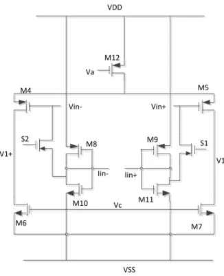
Figures 2.3(a) & (b) show respectively the schematic diagram of the input differential amplifier (DA) stage of the UAM and its small signal equivalent. Transistors M4, M5, M6, M7 & M12 are included in the DA stage. The circuit is designed for bias current level (approximately) of IDM12 =
70 µA, so that each branch have bias current level of IDM5 = IDM4 = 35 µA. Now to obtain this
level in each branch and solving for IDM5 = IDM7 (or IDM4 = IDM6) using the standard square law
equation, the transistor size can be chosen as WM12 = 95 µm, LM12 = 1.2 µm; WM4 = WM5 = 40
µm, LM4 = LM5 = 1.2 µm and WM6 = WM7 = 23.4 µm, LM6 = LM7 = 1.2 µm. As the module
operates both in voltage and current mode, there are provisions for both voltage and current signal inputs. Necessary bias voltage levels are taken from the voltage divider circuit as in figure 2.2.
18 AC + Vsg5 -+ V1 -gm5vsg5 rds5‖rds7 VSS VDD Vc Va M12 M4 M5 M6 M7
Input differential stage Vin+
Vin-V1+
V1-(a)
(b)
Figure 2.3: (a) Schematic diagram of differential input stage (b) Small signal equivalent model of DA stage
Small signal voltage gain of the differential amplifier stage is,
in v
v1
= -gm5 (rds5‖rds7) (2.3)
Using the proper transconductance and resistance values from APPENDIX – F, gain ≈ 56.
Input signal voltage is applied to conventional PMOS differential pairs. For applying current input with the existing configuration for voltage, two complementary gate – drain connected MOS are inserted, output of which is connected with the voltage input leads. Resistance of the gate – drain connected MOS stage is low enough (~200Ω in this case) to apply current input at this node. Current input stage is separated from the voltage input stage by a NMOS switch (S1, S2 in figure 2.4). Hence either voltage or current input stage is selected based on the intended mode of operation, i.e. voltage input stage is selected in case of voltage mode operation and current input
19
stage is selected in case of current mode operation. Figure 2.4 shows the complete schematic diagram of the input stage for applying current signal.
VSS VDD M8 M9 M10 M11 M12 M4 M5 M6 M7 Vin+ Vin-V1+ V1-Iin+ Iin-S2 S1 Vc Va
Figure 2.4: Schematic diagram of the input stage of the UAM
2.4 Intermediate stages
Two more stages are added with the differential input stages for boosting up the gains i.e. voltage gain, current gain, transconductance and transresistance gain. These comprise of transistors M13, M15, M17 & M23. Intermediate stages also shift the dc voltage level so that nominal output DC level is nearly equal to zero volts. Simple common-source amplifier configuration is used as gain boosting stages with PMOS loads. Figures 2.5(a) & (b) show respectively the schematic diagram of the intermediate stages and small signal equivalent model. Bias current level of the M13, M15 column of transistors is, IDM13 = IDM15 = 56 µA and output DC level at the drain of M13 (& M15)
≈ -740 mV. Now using the standard square law equation and solving for IPM13 = INM15 provides,
20 M13 M15 M19 M21 M17 M23 Va VSS VDD To voltage buffer stage From DA stage Compensation circuit + V1 - gm15v1 rds13‖rds15 + V2 -rds17‖rds23 + V3 -V1 V2 V3 (a) (b)
Figure 2.5: (a) Schematic diagram of intermediate stages; (b) Small signal equivalent model
From figure 2.5 (b), small signal gain of the M13, M15 column of transistors can be written as [64], 1 2 v v = -gm15 (rds13‖rds15) (2.4)
Similarly small signal gain of the M17, M23 column of transistors can be written as:
2 3
v v
= -gm23 (rds17‖rds23) (2.5)
Putting the values of appropriate transconductances and resistances (APPENDIX – F) in equations (2.4) and (2.5), gains of these stages become
1 2 V V ≈ 125.11, and 2 3 V V ≈ 149 respectively.
21 2.5 Frequency compensation
A technique using Miller’s theorem is used for frequency compensation of this system. Inserting the compensating capacitance, Cc between two gain stages provides the compensated poles at, P1
≈ -503.8 KHz. Pole frequency is obtained by performing HSPICE simulation using appropriate command (.PZ V(3) Vin; [65]). Formula for the first pole can be expressed as [2]:
P1 = C I II mIIR R C g 1 (2.6)
where, gmII = conductance of M23 = gmM23;
RII = equivalent resistance of transistors M17 and M23 = rds17‖rds23;
RI = equivalent resistance of transistors M13 and M15 = rds13‖rds15
and Cc = Compensating capacitance
Putting the value of these parameters from APPENDIX-F, value of the compensating capacitor, Cc can be calculated from equation (2.6) as, Cc = 71.65 fF. A source – drain connected MOS
(transistor M19) having W = 13 µm, L = 1.2 µm can be used to produce a capacitor of this value. Fig. 2.5 shows the components for pole and zero compensation between two gain boosting intermediate stages.
As the RHP zero results from the feed forward path through the compensation capacitor, it tends to limit the gain-bandwidth of the system. Hence to eliminate the effect of RHP zero, a nulling resistor, Rz is inserted in series with Cc resulting the compensating zero at [2]:
22 z1 = ) 1 ( 1 23 Z m C g R C Considering z1 = p2 = II mM C g 23 , Rz can be calculated as [2], Rz = 23 1 . mM C II C g C C C (2.7)
Using Cc = 71.65 fF and value of CII & gmM23 (from APPENDIX – F), value of Rz can be
calculated rom equation (2.7) as, Rz = 53.11 KΩ. An NMOS (transistor M21) is designed having
W = 1 µm, L = 2.25 µm to operate in resistive mode that provides the value of Rz.
2.6 Voltage buffer stage
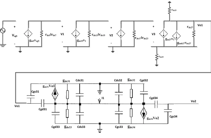
The final stage in the voltage amplifier system is the common drain buffer stage. Figures 2.6 (a) & (b) show respectively the schematic diagram of the voltage buffer stage of the UAM and its small signal equivalent model. This stage comprises of transistors M25, M27 & M29. The purpose of this stage is to drive resistive load or large capacitive load (or a combination of both) [5]. Voltage buffer stage can provide voltage gain with voltage signal input applied at the input stage for voltage and transresistance gain with current signal input applied at input stage for current.
23 M25 M27 M29 To current buffer stage Vc VSS VDD From intermediate stage V3 Voltage output Vo-+ Vo -rds29 rds25 rds27 gm27vgs27 -gmb27v o-+ Vgs27 -(a) (b)
Figure 2.6: (a) Schematic diagram of the voltage buffer stage; (b) Small signal model of the voltage buffer
From figure 2.6 (b), small signal gain of the voltage buffer stage can be written as [64]:
3 v vo = R g g R g mb m m ) ( 1 27 27 27 (2.8) Where, R/ = (rds27+rds25)‖rds29‖ 27 1 mb g
Using the appropriate values of parameters from APPENDIX – F,
73 . 0 3 v vo
2.7 Current buffer stage
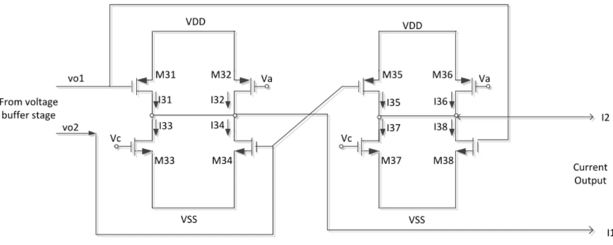
A wideband CMOS transconductor [32] is used as the current buffer stage of the UAM. The purpose of this stage is to provide satisfactory transconductance gain with voltage signal input as well as current gain with current signal input over a wide bandwidth range. Figure 2.7 shows the schematic diagram of the current buffer stage of the UAM comprising transistors M31 – M38.
24 M35 M37 M31 M33 M32 M34 M36 M38 Va Va Vc Vc From voltage buffer stage VDD VDD VSS VSS I1 I2 vo2 vo1 Current Output I31 I32 I33 I34 I35 I36 I37 I38
Figure 2.7: Schematic diagram of the current buffer stage of the UAM
From figure 2.7, using the standard square-law model for the transistors in saturation region, we can write the KCL,
I1 = I31 + I32 – I33 – I34 (2.9a)
and I2 = I35 + I36 – I37 – I38 (2.9b)
Hence, the differential output current,
Iout = I2 – I1 Iout = Vin [2β31(VDD - |VTP|) + 2β34(VSS + VTN)] where, 31 31 31 2 L W Cox p , 34 34 34 2 L W Cox p
; |VTP| and VTN threshold voltages for PMOS and
NMOS respectively. vin is the differential input voltage, i.e. vin = vo1 – vo2. Here M31-M35,
25 Cgs31 Cgd31 Cds31 Cgd33 gds33 Cds33 I1 Cds32 Cgs33 Cgd32 gds34 Vo1 Vo2 gm31Vo1 gm34Vo2 Cgd34 Cgs34
Figure 2.8: Small signal equivalent model of the transconductor
Figure 2.8 shows the small signal equivalent model of the transconductor as shown in figure 2.7. From the figure, equation of output AC current can be written as:
-i1 = gm31vo1 + gm34vo2 – sCgd31vo1 – sCgd34vo2 (2.10a)
Similarly for the other half circuit,
-i2 = gm35vo2 + gm38vo1 – sCgd35vo2 – sCgd38vo1 (2.10b)
Differential small signal output current can be calculated as [66], iout = i2 – i1
iout = 2(gm38 – gm31) vo1 (2.11)
Hence, by putting the transconductance values of M38 & M31 (from APPENDIX – F) and value of vo1 from the voltage buffer stage, output AC current can be calculated from equation (2.11) as,
26 2.8 The Universal Amplifier Module (UAM)
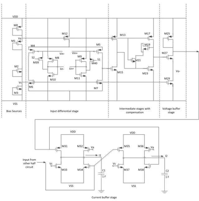
Combining all the sub systems i.e. the input differential stages, intermediate stages, compensation circuit, voltage buffer stage and current buffer stage provide the complete schematic diagram of the proposed universal amplifier module (UAM). The complete schematic diagram of the UAM is shown in figure 2.9.
VSS VDD Vc Va M0 M1 M2 M3 M8 M9 M10 M11 M12 M4 M5 M6 M7 M13 M15 M19 M21 M17 M23 M25 M27 M29
Bias Sources Input differential stage Intermediate stages with compensation Voltage buffer stage S2 S1 M35 M37 M31 M33 M32 M34 M36 M38 Va Va Vc Vc Input from other half circuit VDD VDD VSS VSS
Current buffer stage Vin+ Vin-Iin+ Iin- Vo-C1 C2 1 F 1 F I1 I2 M39 M40
27
The proposed Universal Amplifier Module (UAM) takes both voltage and current signal input and provides both voltage and current signal output, hence providing all types of voltage and current mode operations i.e., the UAM is capable of providing VCVS, VCCS, CCVS and CCCS operations. Hence the module is named as the universal module.
2.9 Voltage and current – mode operations of the UAM
In this section the operations of the UAM as VCVS, VCCS, CCVS and CCCS are described with some basic formulas and appropriate small signal equivalent circuit models.
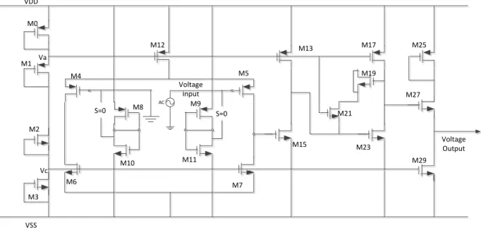
2.9.1 Implementation of VCVS using the UAM
Figure 2.10 shows the VCVS implementation of the UAM. 1 V AC is applied across the input differential PMOS transistors. Voltage signal output is taken from the voltage buffer stage. Figure 2.11 shows the small signal equivalent model of the VCVS.
28 Voltage Input VSS VDD Vc Va M0 M1 M2 M3 M8 M9 M10 M11 M12 M4 M5 M6 M7 M13 M15 M19 M21 M17 M23 M25 M27 M29 S=0 S=0 Voltage Output AC
Figure 2.10: Schematic diagram of the half circuit of VCVS implementation of the UAM
AC + Vsg5 -gm5vsg5 rds5‖rds7 + V1 - gm15v1 rds13‖rds15 + V2 -rds17‖rds23 + V3 -+ Vo -rds29 rds25 rds27 gm27vgs27 -gmb27v o-gm23v2
Figure 2.11: Small signal equivalent circuit of the UAM configured as VCVS
From figure 2.11, overall AC gain can be written as:
Av = in o v v = 3 v vo . 2 3 v v . 1 2 v v . in v v1 (2.12)
29
Now putting the values from equations (2.3), (2.4), (2.5) & (2.8) into equation (2.12),
Av = [-gm5 (rds5‖rds7)].[-gm15 (rds13‖rds15)].[-gm23 (rds17‖rds23)].[ R g g R g mb m m ) ( 1 27 27 27 ] (2.13)
Hence, using the appropriate conductance and resistance values from APPENDIX – F, value of overall gain of the VCVS can be calculated from equation (2.13) as, Av = 794.33 K ≈ 118 dB.
2.9.2 Implementation of CCVS using the UAM
Gate – drain connected stage is added at the input of the same existing VCVS circuit to apply current so that there is a small impedance node at the input. Figure 2.12 shows the schematic diagram of the UAM that works as CCVS (i.e. a trans-resistance device).
VSS VDD Vc Va M0 M1 M2 M3 M12 M4 M5 M6 M7 M13 M15 M19 M21 M17 M23 M25 M27 M29 Voltage Output M9 M10 M11 Current Input S=1 S=1
Figure 2.12 Schematic diagram of CCVS implementation of the UAM
Similar small signal equivalent model can be drawn to express the transresistance gain. As, a gate – drain connected stage is added with the existing configuration of VCVS, hence there will
30
be an additional resistance at the input stage parallel with the input current source. Figure 2.13 shows the small signal equivalent half – circuit of the CCVS system.
+ Vsg5 - gm5vsg5 rds5‖rds7 + V1 - gm15v1 rds13‖rds15 + V2 -rds17‖rds23 + V3 -+ Vo -rds29 rds25 rds27 gm23V2 -gmb27v o-iin r ds9‖rds11 gm27vgs27
Figure 2.13: Small signal equivalent circuit of CCVS configuration
From figure 2.13, small signal voltage gain of stage 1 is,
5 1 sg v v = -gm5 (rds5‖rds7) (2.14)
Now overall voltage gain can be calculated as:
Av = 5 sg o v v = 3 v vo . 2 3 v v . 1 2 v v . 5 1 sg v v (2.15)
Now vgs5 can be written as,
vsg5 = (rds5‖rds7) iin
Putting the value of vsg5 into equation (2.15),
in ds ds o i r r v ) ( 5 7 = 3 v vo . 2 3 v v . 1 2 v v . 5 1 sg v v
31
Hence, the overall transresistance gain of the CCVS will be,
Rm = in o i v = 3 v vo . 2 3 v v . 1 2 v v . 5 1 sg v v (rds5‖rds7) (2.16)
Plugging the values from equations (2.4), (2.5), (2.8) & (2.14) into equation (2.16),
Rm = [-gm5 (rds5‖rds7)][-gm15 (rds13‖rds15)][-gm23 (rds17‖rds23)]. R g g R g mb m m ) ( 1 27 27 27 (r ds5‖rds7) (2.17)
Hence, using the values of gm and rds of the appropriate transistors from APPENDIX – F, value
of overall transresistance gain of the CCVS can be calculated from equation (2.17) as, Rm =
179.27 MΩ ≈ 165.07 dBΩ.
2.9.3 Implementation of VCCS using the UAM
M35 M37 M31 M33 M32 M34 M36 M38 Va Va Vc Vc Input from other half circuit VDD VDD VSS VSS Vo1 I1 I2 Vo2 Vo1 Current Output I31 I32 I33 I34 I35 I36 I37 I38 Voltage Input VSS VDD Vc Va M0 M1 M2 M3 M8 M9 M10 M11 M12 M4 M5 M6 M7 M13 M15 M19 M21 M17 M23 M25 M27 M29 S=0 S=0 AC
32
Figure 2.14 shows the diagram of the VCCS implementation of the proposed Universal Amplifier Module (UAM). Voltages, vo1 & vo2 from the output voltage buffer stage of two
differential half circuits are fed to the transconductor. The transconductor converts the difference of the voltages (i.e. vo1 – vo2) into equivalent current.
AC + Vsg5 -gm5vsg5 rds5‖rds7 + V1 - gm15v1 rds13‖rds15 + V2 -rds17‖rds23 + V3 -rds29 rds25 rds27 gm27v3 gmb27vbs27 Cgs31 Cgd31 gds31 Cds31 Cgd33 gds33 Cds33 I1 Cds32 Cgs33 Cgd32 gds32 gds34 Vo1 Vo2 gm31Vo1 gm34Vo2 Cgd34 Cgs34 Vo1
Figure 2.15: Small signal equivalent model of the half circuit of VCCS
Figure 2.15 shows the small signal equivalent model of the half circuit of the VCCS. From the figure, vo1 is taken from the drain terminal of M27, hence working as a common-source amplifier
with source degeneration. In this case, Small signal gain of this stage is [64],
3 1 v vo = - 29 27 27 25 27
)
(
1
m mb ds ds mr
g
g
r
g
(2.18)33
Hence overall gain can be calculated as,
in o v v1 = 3 1 v vo . 2 3 v v . 1 2 v v . in v v1 (2.19)
Using the values from equation (2.3), (2.4), (2.5) & (2.18) and putting into equation (2.19),
in o v v1 =
]
)
(
1
[
29 27 27 25 27 ds mb m ds mr
g
g
r
g
[-gm23 (rds17‖rds23)].[-gm15 (rds13‖rds15)].[-gm5 (rds5‖rds7)] Hence, vo1 =]
)
(
1
[
29 27 27 25 27 ds mb m ds mr
g
g
r
g
[-gm23 (rds17‖rds23)].[-gm15 (rds13‖rds15)]. [-gm5 (rds5‖rds7)] vin (2.20)Now from equation (2.11) output AC current is already calculated as: iout = 2(gm38 – gm31) vo1
Putting the value of vo1 from equation (2.20),
iout = 2(gm38 – gm31)
]
)
(
1
[
29 27 27 25 27 ds mb m ds mr
g
g
r
g
.[-gm23 (rds17‖rds23)]. [-gm15 (rds13‖rds15)].[-gm5 (rds5‖rds7)] vinHence, the overall transconductance gain of the VCCS is,
Gm = in out v i = 2(gm38 – gm31)
]
)
(
1
[
29 27 27 25 27 ds mb m ds mr
g
g
r
g
.[-gm23 (rds17‖rds23)]. [-gm15 (rds13‖rds15)].[-gm5 (rds5‖rds7)] (2.21)34
So using the appropriate transconductance and resistance values from APPENDIX – F, overall transconductance gain of the CCVS can be calculated from equation (2.21). The value in case of the UAM is, Gm = 2.296 A/V ≈ 7.22 dBA/V.
2.9.4 Implementation of CCCS using the UAM
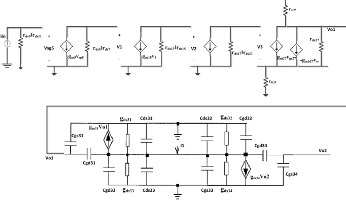
VSS VDD Vc Va M0 M1 M2 M3 M12 M4 M5 M6 M7 M13 M15 M19 M21 M17 M23 M25 M27 M29 M9 M10 M11 Current Input M35 M37 M31 M33 M32 M34 M36 M38 Va Va Vc Vc Input from other half circuit VDD VDD VSS VSS I1 I2 vo2 vo1 Current Output I31 I32 I33 I34 I35 I36 I37 I38 S=1 S=1
Figure 2.16: Schematic diagram of CCCS implementation of the UAM
Figure 2.16 shows the diagram of the CCCS implementation of the proposed Universal Amplifier Module (UAM). Signal current is applied at the gate – drain connected input stage. This current produces a voltage vo1 & vo2 at the output voltage buffer stage of two differential
35
stage. Similar small signal equivalent model can be drawn for the CCCS circuit. Figure 2.17 shows the half circuit of the AC equivalent model of the circuit as in figure 2.16.
gm5vsg5 rds5‖rds7 + V1 - gm15v1 rds13‖rds15 + V2 -rds17‖rds23 + V3 -rds29 rds25 rds27 gm27vgs27 -g mb27v o-Cgs31 Cgd31 gds31 Cds31 Cgd33 gds33 Cds33 I1 Cds32 Cgs33 Cgd32 gds32 gds34 Vo1 Vo2 gm31Vo1 gm34Vo2 Cgd34 Cgs34 + Vsg5 -Iin rds9‖rds11 Vo1
Figure 2.17: Small signal equivalent model of the half circuit of CCCS
From the above figure, we get the voltage gain expression as:
5 1 sg o v v = 3 v vo . 2 3 v v . 1 2 v v . 5 1 sg v v (2.22) Now using (2.15), 5 1 sg o v v =
]
)
(
1
[
29 27 27 25 27 ds mb m ds mr
g
g
r
g
[-gm23 (rds17‖rds23)]. [-gm15 (rds13‖rds15)].[-gm5 (rds5‖rds7)] Hence, vo1 =]
)
(
1
[
29 27 27 25 27 ds mb m ds mr
g
g
r
g
.[-gm23 (rds17‖rds23)].[-gm15 (rds13‖rds15)].36
[-gm5 (rds5‖rds7)]vsg5 (2.23)
Now putting the value of vsg5 = (rds5‖rds7) iin into equation (2.23),
vo1 =
]
)
(
1
[
29 27 27 25 27 ds mb m ds mr
g
g
r
g
. [-gm23 (rds17‖rds23)].[-gm15 (rds13‖rds15)]. [-gm5 (rds5‖rds7)].(rds5‖rds7) iin (2.24)Now from equation (2.11), output AC current,
iout = 2(gm38 – gm31) vo1
Putting the value of vo1 from equation (2.24) implies,
iout = 2(gm38 – gm31).
]
)
(
1
[
29 27 27 25 27 ds mb m ds mr
g
g
r
g
. [-gm23 (rds17‖rds23)].[-gm15 (rds13‖rds15)]. [-gm5 (rds5‖rds7)].(rds5‖rds7) iinHence overall current gain of the CCCS circuit will be,
Ai = in out i i = 2(gm38 – gm31).
]
)
(
1
[
29 27 27 25 27 ds mb m ds mr
g
g
r
g
. [-gm23 (rds17‖rds23)].[-gm15 (rds13‖rds15)]. [-gm5 (rds5‖rds7)].(rds5‖rds7) (2.25)The numerical value of the gain can be calculated from equation (2.25) using transconductance and resistance of appropriate transistors from APPENDIX – F. The value of current gain in this case is, Ai = 520 ≈ 54.32dB.
37 2.10 Summary
This chapter introduced different sub-systems of the UAM with their proper functions. The gain expressions for the four different categories of amplifiers (i.e., VCVS, VCCS, CCVS, and CCCS) are produced and the respective numerical values are provided. The theoretical analysis should be validated using suitable simulations and experimental works. In the next chapter, simulations of the UAM are provided to validate the proposed voltage and current mode implementations of the UAM.
38
CHAPTER
3
CHARACTERIZATION
OF
THE
UAM
USING
SIMULATIONS
3.1 Introduction
In the previous chapter, the design and analysis aspects corresponding to different sub-systems of the UAM have been presented. The techniques to adopt the UAM for the four basic categories of amplifiers (i.e., VCVS, VCCS, CCVS and CCCS) have been shown as well. Theoretical formulas for the gains of the basic amplifiers and the respective numerical values have been provided.
To validate the theoretical analysis, suitable simulations and experimental works are necessary. This chapter presents simulation results pertaining to the operations of the UAM as the four categories of amplifiers. Different performance parameters are measured by SPICE simulations. The simulations are performed at the schematic level followed by post layout simulations. The layout has been implemented using 0.18 µm CMOS (CMOSP18/TSMC) process.
39 3.2 Complete Schematic of UAM
Figure 3.1 shows the complete schematic diagram of the proposed Universal Amplifier Module (UAM) in 0.18 µm CMOS (CMOSP18/TSMC) technology.
Figure 3.1: Complete schematic diagram of the UAM in 0.18 µm CMOS (CMOSP18/TSMC) technology
The UAM is now capable of providing all the voltage and current mode operations with just a single module. Either voltage or current signal input can be chosen by the switch, S. Two NMOS pass transistors are used as switch (S).
The switch (S) is:
‘ON’ when Vgsn = VDD, i.e. S = 1
40
When the switch is ‘ON’, then the gate – drain connected transistors M8, M9, M10 & M11 (shown in figure 2.4) are connected across the input differential stages. Hence, there is a low impedance node at the input stages and a signal current can be applied at this node.
When the switch (S) is ‘OFF’, the gate – drain connected stage is disconnected from the input differential stages. Hence, a voltage signal can be applied to the input of the differential voltage amplifier section (comprising of transistors M4, M5, M6 & M7).
Selection of the switch (S) depends on the intended use of the mode of operations. Hence, S = 0 is set for voltage signal mode of operations, i.e. for VCVS and VCCS operations. On the other hand, S = 1 is set for current signal mode of operations, i.e. for CCVS and CCCS operations. Voltage signal output is taken from the voltage buffer stage (comprising of transistors M25, M27 and M29 as shown in figure 2.6) which is a low impedance node. The current signal output is taken from the current buffer stage (comprising of transistors M31 – M38 as shown in figure 2.7) which is a high impedance node.
3.3 Dimensions of the transistors
The transistors in the half circuit of the Universal Amplifier Module (UAM), shown in figure 2.9 of chapter 2, have the dimensions presented in Table 3.1.
41
Table 3.1: Dimensions of the transistors used in UAM
TRANSISTORS W (µm) L (µm) M0, M1, M27 20 1.2 M2, M3 10 1.2 M4, M5 40 1.2 M6, M7 23.4 1.2 M8, M9 74.16 1.2 M10, M11, M19 13 1.2 M12 95 1.2 M13 70 1.2 M15 11.88 1.2 M17 37 1.2 M21 1 2.25 M23 10.08 1 M25 9 1.2 M29 7.7 1.2 M31, M35 65 1.5 M32, M36 70 1.5 M33, M34, M37, M38 1.5 1.5 M39, M40 30 1.2
3.4 Performance parameters measurements
Simulations were done for all the voltage and current mode operations (i.e. VCVS, VCCS, CCVS and CCCS). Due to page limitations, only simulations of VCVS are presented in this section. At the same time, all the voltage and current mode simulation results are given in tabular format. Figure 3.2 shows the UAM as a block representation used for the simulations to measure various performance parameters.
42
Measurements for VCVS (i.e., operational amplifier, OP-AMP) Configuration: 3.4.1 Open loop frequency response
Vin = 1 V AC is applied at the voltage input section. The switch, S is set to OFF mode (i.e., S=0).
UAM Vin-Vin+ Iin-Iin+ Vo-Vo+ Io-Io+ VSS VDD S AC Vo-Vo+
Figure 3.2: Configuration for open loop frequency response
The frequency plot, called as bode plot gives an estimation of open loop voltage gain and phase response. It also shows the occurrence of poles, zeros, unity gain bandwidth, 3dB frequency etc. The phase margin and gain margin of the VCVS can also be calculated from the frequency response. Figure 3.3 shows the magnitude and phase response of the VCVS. From the figure, voltage gain, Av = 118 dB (for vo-). From the other half circuit it can be shown that, voltage gain
![Figure 1.5 shows the block diagram of important sub systems of an OP-AMP [5].](https://thumb-us.123doks.com/thumbv2/123dok_us/1871190.2773106/22.918.218.705.505.723/figure-shows-block-diagram-important-sub-systems-amp.webp)