Telecomunicaci´
o de Barcelona
Master Thesis
Light sensor development for Ara
platform
Author:
AlexisDUQUE
Supervisor: Pr. JosepParadells Aspas
Wireless Network Group
Escola T`ecnica Superior d’Enginyeria de Telecomunicaci´o de Barcelona
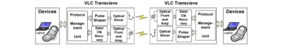
During the last years, Visible Light Communication (VLC), a novel technology that enables standard Light-Emitting-Diodes (LEDs) to transmit data, is gaining significant attention. In the near future, this technology could enable devices containing LEDs – such as car lights, city lights, screens and home appliances – to carry information or data to the end-users, using their smartphone. However, VLC is currently limited by the end-point receiver, such as a the mobile camera, or a peripheral connected through the jack input and to unleash the full potential of VLC, more advanced receiver are required.
On other, few year ago, Google ATAP - the Google innovation department - announced the Ara initiative. This consist on a modular phone where parts of the phone, like cameras, sensors or networks can be changed. So when a new feature appears or required by the user it is not needed to change the mobile phone, just to buy the modules with the functionality.
This Master Thesis presents the design and development of a simple module that will support communication by light (VLC) using the Ara Module Developer Kit provided by Google. It consists on building a front-end circuit, connecting a photodiode that receives the level of light and use it as data carrier, in order to receive and display data inside a custom Android application on the Ara smartphone.
To my supervisor, Josep Paradells which trust me and give me the opportunity to work on this project.
To the Wireless Network Group team for there guidance and everyday help and support. To Miguel and Cleo, my hosts during these five past months in Barcelona.
List of Tables viii Abbreviations ix 1 Introduction 1 1.1 Motivations . . . 1 1.2 Objectives . . . 2 1.3 Report Organization . . . 3 2 Technical background 4 2.1 VLC Standard . . . 4 2.2 VLC Technology . . . 4
2.2.1 Modulation and transmitter . . . 5
2.2.2 Receivers . . . 8
2.2.3 Run-length limited coding . . . 9
2.2.3.1 Manchester . . . 10
2.2.3.2 4B6B . . . 10
2.3 ARA Platform . . . 12
2.3.1 Introduction to the ARA project . . . 12
2.3.2 Project goals . . . 12
2.3.3 Structure and features . . . 12
2.3.4 Project team . . . 13
2.3.5 History and development process . . . 14
2.3.6 Module Development Kit Architecture . . . 14
2.3.6.1 Android AP board . . . 14
2.3.6.2 Endoskeleton Switch Dev Board . . . 14
2.3.6.3 GP Endpoint board . . . 15
2.3.6.4 MDK Configuration and Setup . . . 16
3 State of the Art 17
3.1 VLC Implementations . . . 17
3.1.1 Visible Light Road-to-vehicle Communication Using High-Speed Camera . . . 17
3.1.2 Integrated System of White LED Visible-Light Communication and Power-Line Communication . . . 18
3.1.3 Visible Light Communication for Advanced Driver Assistant Systems 19 3.1.4 Study of Visible Light Communication System Using RGB LED Lights . . . 19
3.2 Smartphone solutions . . . 20
3.2.1 Visible Light Communication using smartphone camera and rolling shutter effect . . . 20
3.2.2 Visible Light Communication using smartphone ambient light sensor 20 4 Proposal 22 4.1 System Description . . . 22
4.2 VLC Contribution . . . 23
5 Project Description 25 5.1 ARA platform study . . . 25
5.1.1 MDK and boards study . . . 25
5.1.2 Android for ARA reliable I/O operation rate . . . 25
5.1.2.1 Problematic . . . 25
5.1.2.2 Experiments with the Oxymeter module and an Arduino 26 5.1.2.3 Results . . . 26
5.1.2.4 Conclusion . . . 27
5.1.3 ARA benchmark . . . 27
5.1.3.1 Conclusion . . . 28
5.2 Receiver circuit design . . . 29
5.2.1 Needs description . . . 29
5.2.2 1st Op-Amp : Trans-Impedance Amplifier . . . 29
5.2.3 2nd: High Pass filter . . . 30
5.2.4 Gain . . . 30 5.3 Emitter driver . . . 31 5.3.1 Micro-Controller Unit . . . 32 5.3.2 OOK modulation . . . 32 5.3.3 4B6B Line coding . . . 32 5.3.4 Transmission Pattern . . . 33 5.3.5 Algorithm . . . 34
5.4 Receiver ADC and Buffer . . . 34
5.4.1 Hardware choice . . . 34
5.4.2 Software implementation . . . 35
5.4.2.1 Data Acquisition . . . 35
5.4.2.2 Demodulation and RLL Decoding . . . 35
5.4.2.3 Buffering . . . 36
5.4.2.4 Input/output . . . 36
6.5 Discussion . . . 44
7 Conclusion 45
7.1 Achieved work . . . 45
7.2 Future works . . . 45
A ARA development kit documentation 50
B Circuit Schematics 55
C Emitter software sources 56
D Receiver software sources 86
E Java software sources 119
F JNI software sources 129
2.1 Manchester encoding . . . 10
2.2 VLC Receiver front-end circuit . . . 11
2.3 ARA Application Processor Board . . . 15
2.4 ARA Endoskeleton Switch Board . . . 15
2.5 Module to Module Communication (with Native UniPro Support and Bridge ASICs) . . . 16
2.6 ARA Generic Endpoint Board . . . 16
3.1 Road-to-vehicle visible light communication . . . 18
3.2 Waveform on power-line . . . 18
3.3 General architecture for a full duplex VLC system . . . 19
3.4 FIRE use case . . . 21
4.1 Proposal hardware implementation . . . 23
4.2 VLC system proposal . . . 24
5.1 Probability density of Android thread execution interval with 20ms as defined period . . . 26
5.2 Probability density of Android thread execution interval with 50ms as defined period . . . 26
5.3 CPU load and allocation with only Oxymeter application running. Pro-cess on the left are system thread. . . 28
5.4 CPU load and repartitions during the web browsing simulation . . . 28
5.5 Trans-Impedance Amplifier . . . 30
5.6 High-Pass Filter . . . 31
5.7 High-Pass Filter Bode Plot . . . 31
5.8 Gain Operational Amplifier . . . 32
5.9 Android application receiving data via VLC . . . 38
6.1 The ARA MDK and its VLC receiver module . . . 41
6.2 Receiver illumination over the distance . . . 42
6.3 In yellow the signal just after the TIA. In blue, the signal after analogical filtering - 2,5 meter distance . . . 42
6.4 In red the signal sampled. In blue, the bits computed after digital pro-cessing and demodulation . . . 43
6.5 In blue, the signal generated by the LED driver. In yellow, the signal after our circuit - 2,5 meter distance - 360kHz . . . 44
B.1 VLC Receiver front-end circuit . . . 55
2.1 Manchester RLL code . . . 10
2.2 4B6B RLL code . . . 11
5.1 DAC needs summary . . . 28
5.2 Modified 4B6B . . . 33
5.3 A transmission example : 2 16 bits . . . 34
6.1 Bit Error Rate for different clock rate at 2,5 meters, using 4B6B coding . 43 6.2 Bit Error Rate for different clock rate at 2,5 meters, using Manchester coding . . . 44
Op-Amp Operational Amplifier
OS OperatingSystem
OOK OnOff Keying
PTM PulseTimeModulation
PAM PulseAmplitudeModulation
PWM PulseWidth Modulation
RAM Random AccessMemory
SDK Software Developement Kit
TIA TransImpedanceAmplifier
UART UniversalAsynchronous ReceiverTransmitter
VLC Visible LightCommunication
Introduction
1.1
Motivations
For the last century, radio frequency (RF) has dominated wireless communications.But RF has been a victim of its own success. The number of mobile devices and embedded
systems has increased tremendously as technology becomes a primary need in peoples lives. This explosion of mobile devices comes at a cost:the frequency spectrum is a scarce
resource. The massive increase in RF communicating devices is leading to a saturation of the available bandwidth, which will result in a drop of quality-of-service.
To ameliorate the bandwidth saturation problem, the research community has been exploring other wireless technologies. One of the most promising alternatives is visible
light communication. Light is electromagnetic radiation just like RF, but the difference lies in frequency. Because of this frequency, the interaction between light and matter is
different on a fundamental level which gives light unique properties.
With the advent of Visible Light Communication (VLC), the widespread exploitation of
the visible light spectrum is becoming a reality. VLC enables standard Light Emitting Diodes (LEDs) to transmit data wirelessly, and this is an important step because LEDs
are permeating our daily environments at a very fast pace.
After intensive research into energy consumption, in 2009 the European Union and other
countries started measures to phase out incandescent light bulbs in favor of high efficient LEDs. But it is not only residential and commercial lighting that is being replaced with
approach using an external peripheral as VLC receiver, plug-in it to the jack mobile phone or through Bluetooth [1].
Thus, considering that VLC can potentially transform any LED device into a wireless
transmitter there may be a new generation of objects waiting to be connected to people smartphone.
1.2
Objectives
However, actual research and VLC implementation on mobile phone are highly limited by receiver hardware. In fact, embedded sensor on smartphone, such as camera are not
appropriate for sensing modulated light. External peripheral, adding an other channel reduce considerably the throughput. That why, the recent concept of modular
smart-phone, called Phonebloks (2013) and industrialized as Project Ara y Google, could be the solution.
Project Ara is an effort in Google’s Advanced Technology Projects (ATAP) organization to create a modular smartphone platform, with the twin aims of delivering a deep
customization experience to users and enabling significantly lowered barrier to entry into the mobile hardware ecosystem.
This project aims to take advantage of this new technology developing a Visible Light
Communication receiver for the Ara plartform. Major objectives are listed below :
• Design and develop a module that support visible light communication.
• Determine the Ara smartphone possibility for future work on wireless
• Develop a convenient LED driver suited for our need.
• Experiment a communication between a LED emitter and the modular
smart-phone.
1.3
Report Organization
Chapter 1 of this report serves to provide an introduction of the basic concepts and
techniques and also shows several designs that are required for the implementation of VLC.
Chapter 2 provides the background needed for the VLC designs. Chapter 3 provides the literature review of the VLC technology.
Chapters 4 and 5 provide our proposal description and the experimental setup and implementation of the models.
Chapter 6 presents our results and recommendations for improving the designs as well
VLC as we know it today would not be possible without LEDs. Before we introduce our proposal, we provide background information about LEDs as wireless transmitter, then we describe the many ways in which light intensity can be modulated and received, and
the line coding scheme used in indoor VLC.
2.2
VLC Technology
Modulation of light has been used for centuries. In 1792 the French inventor Claude
Chappe invented the optical telegraph, a system of towers with signaling devices, which allowed Napoleon to pass messages throughout his empire. Although simple and
prac-tical, these systems are the ancestors of VLC. For some decades after these events, light communication in the form of morse was used, but further development of light
commu-nication stood still because with incandescent lamps the data rates pale in comparison to what could be achieved with radio. In the same way, Infrared(IR) has been introduced
for a long time, but they are limited to Line-Of-Sight (LOS), with a very short range use case, and are very sensitive to the weather or obstacles.
It is only until recently that we have a pervasive infrastructure that can modulate light to achieve data rates that are meaningful for today’s communication needs. Due to recent
advancements in LED technology we can transform light bulbs into high speed wireless
transmitters. Data can be modulated in every light source using changes in intensity, but only certain light sources possess the necessary properties to transmit high data
rates.
Fundamentally, modulating light requires changes of light intensity. For the last century
incandescent lamps have been the primary source of light, but incandescent light cannot comply with high speed modulation because of the mechanism it uses to generate light.
Incandescence is the effect of emitting thermal radiation from matter as a result of its temperature. In incandescent light bulbs a wire is heated by running a current through
it, and the resistance of this wire forms kinetic energy which is released in the form of light. This means that intensity control of incandescent lamps takes place through two
steps, resulting in indirect control of the signal. This would not be a problem if the thermal inertia would not make the system too slow for high speed modulation, but it
does.
In the case of LEDs, the direct relation between intensity and electricity permit high
speed modulation. LEDs consist of a semiconductor material that contains excited
electrons. A fundamental property of electrons is that when they are forced into a lower
energy state they release their energy in the form of the emission of photons. This effect is called electroluminescense and gives direct control over light intensity through
the control of voltage and current. A simple circuit with transistors can deliver the necessary control of current, and this makes the changes in light intensity fast enough
to transfer information at a high data rate.
An alternative to LEDs is laser. Lasers can also be controlled at high speed, and have
the additional capability of strengthening the electroluminescense effect by amplifying and focusing the generated light. This makes laser a good candidate for long range
communication, but for short distances its transmission angle is too narrow (and hence it can be easily obstructed) without using lenses. Another important disadvantage of
laser is that poses health hazards to human beings.
2.2.1 Modulation and transmitter
The light emitted by LEDs can be modulated in different forms, and there are also
modulation is not the same. We will briefly describe this point to make the reader aware
of the fundamental difference in modulation between radio and VLC.
In radio, frequency modulation changes the frequency of the waves in the electromagnetic
field, and amplitude modulation changes the height of this waves. In VLC, amplitude modulation works the same way as in radio, and it is often called intensity modulation.
Frequency modulation however, is very hard to apply with visible light. It can be done but requires advanced laser setups to change the signal’s properties, like phase and
frequency, through interference.
There are many different modulation schemes used for VLC, and we will now discuss
the most commonly used.
1. On-Off-Keying (OOK), or amplitude shift keying, uses keying (switching) to turn
a carrier signal on and off. OOK has a low processing burden but is proven to be very sensitive to noise. Enhanced schemes like On-Off-Keying Non-Return-to-Zero
have shown data rates of 1.5 Gigabits per seconds, using a Integrated Circuit with LEDs bonded into the chip [2].
2. Pulse Time Modulation (PTM) is a technique in which data is modulated in the
ratio between the on and off time of the carrier signal. Pulse Position Modulation (PPM) and Pulse Width Modulation (PWM) fall into this category. The advantage
of PTM is that it does not require digital-to-analog converters to generate a smooth output signal, and does not require an analog-to-digital converter either but only
a comparator circuit. On the other hand, PTM requires accurate timing for both the receiver and transmitter because the ratio between on and off periods needs
and dimming support without additional techniques, which is good for use in illumination devices, but speeds are lower than with other modulation systems [3].
3. Pulse Amplitude Modulation (PAM) uses brightness levels to realize multilevel
signals to encode symbols. This modulation is sensitive to external light sources as they influence the intensity, and has relative low speeds compared to other
techniques. Dimming control can easily be implemented in PAM by changing the probability of the constellation points [4]
4. Frequency Shift Keying (FSK) looks a lot like On-Off-Keying, but instead of
switching a carrier on and off, the system switches between two frequencies. This switch in frequency can be in terms of color i.e. a one is red and a zero is blue, or
in pulse frequency.
5. Phase Shift Keying (PSK) encodes symbols by changing the phase of the light
intensity that has been shaped into a sinusoidal form. Many variants of PSK exist, depending on the number of constellation points used (Binary PSK uses
2 points, 0°and 180°, Quadrature PSK uses 4 points). PSK can be used as base
modulation, but can also be used in combination with other techniques like OFDM
to improve certain weaknesses like intersymbol interference [5].
6. Orthogonal Frequency Division Multiplexing (OFDM) is a technique that uses a large number of modulated carriers with sufficient frequency spacing so that
they are orthogonal. Again, this frequency is modulated through intensity. The strongest advantage of OFDM is that it provides resistance to multipath effects,
which result in long distances and high speed data transfers. Data rates beyond 3
Gigabit per seconds have been reported at short distances ≈10cm) [6].
Unfortu-nately such high speeds demand require high-speed processing units.
7. Quadrature Amplitude Modulation (QAM) is a modulation scheme that conveys bit streams by changing the amplitudes of two or more independent carrier signals,
which results in a spectral efficient scheme. A form of QAM is the Carrier-less Amplitude and Phase (CAP) modulation, a promising high speed VLC modulation
scheme capable of transmitting at 3.22 gigabits per second using an RGB-type led. QAM and CAP can both be combined with OFDM to improve its performance
2.2.2 Receivers
While on the transmitter side the most widely used element is the LED, on the receiver side we have several options: cameras, photodiodes and phototransistors, and LEDs
themselves. The common name for these types of sensors is photodetectors and they use the same fundamental principle, the photoelectric effect: many metals release electrons
when light shines upon it. Although these sensors share the same effect, they have subtle differences that result in unique characteristics.
1. Cameras can detect light, its intensity and its color, using an array of semiconduc-tor junctions or capacisemiconduc-tors. As the miniaturization of cameras continues they can
be found in embedded systems like mobile phones, allowing them to receive vlc signals without additional hardware [9]. Cameras have the advantage of focusing
on the transmission source by looking at specific pixels, so it becomes possible to select a specific VLC source or to ignore a noise source. As a receiver for VLC,
cameras have the disadvantage of requiring more processing to retrieve the signal from the image sensor. Secondly, a bigger disadvantage is the frame rate which is
limited by the camera’s (electronic or mechanic) shutter speed, which limits the signal sample rate and thus the data transfer rate. There are high speed cameras
which offer a solution to this problem, but currently they are too big and power hungry to use in embedded devices.
2. Photodiodes and phototransistors work based on the same principle but their
two. This semiconductor junction is exposed through a transparent casing, so pho-tons can reach the junction and, when having the right frequency, excite
electron-hole pairs which results in a current and voltage. Because of the big surface of the semiconductor junction, photodiodes and phototransistors are very sensitive
to light. When comparing photodiodes to phototransistors, diodes are faster due to the single junction giving it a fast response time. On the other hand,
photo-transistors have a bigger signal gain which results in a stronger electric signal. A disadvantage of photodiodes is the dedicated circuitry needed for amplification,
filtering and sampling to be able to receive a clear electronic signal. Advances in technology are capable of integrating these into a single chip which can alleviate
this disadvantage.
3. LEDs can be used as light sensors. An attentive reader may have noticed that photodiodes and LEDs exploit an oppose effect: while in photodiodes photons
that strike the material generate a flow of electrons, in LEDs a flow of electrons release photons (light). This reversed and complementary effect can be used to
make an LED both a receiver and a transmitter of VLC [10].
Considering the various options for receivers, we opted for photodiodes because they have the higher potential to achieve high data rates, are more sensitive than
other sensors.
2.2.3 Run-length limited coding
Line coding technique are used to send arbitrary data over a communications channel
with bandwidth limits. It bounds the length of stretches (runs) of repeated bits during which the signal does not change If the runs are too long clock recovery is difficult, while
if they are too short, the high frequencies components that are more attenuated by the communications channel.
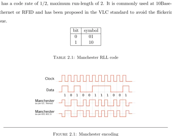
IEEE 802.15.7 standard suggests different RLL codes for VLC PHY I, that can be used with OOK or VPPM modulation.
It has a code rate of 1⁄2, maximum run-length of 2. It is commonly used at 10Base-T Ethernet or RFID and has been proposed in the VLC standard to avoid the flickering issue.
bit symbol
0 01
1 10
Table 2.1: Manchester RLL code
Figure 2.1: Manchester encoding
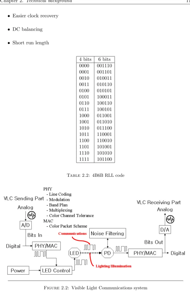
2.2.3.2 4B6B
4B6B expands 4-bit codes to 6-bit symbols with same ratio of 1 and 0 (3:3) and 50 percent duty cycle It supports clock recovery and DC-balanced waveform.
4B6B main advantages are :
• Free from intra-frame flickering
• Easier clock recovery
• DC balancing
• Short run length
4 bits 6 bits 0000 001110 0001 001101 0010 010011 0011 010110 0100 010101 0101 100011 0110 100110 0111 100101 1000 011001 1001 011010 1010 011100 1011 110001 1100 110010 1101 101001 1110 101010 1111 101100 Table 2.2: 4B6B RLL code
modules or upgrade individual modules as innovations emerge, providing longer lifetime cycles for the handset, and potentially reducing electronic waste. Project Ara
smart-phone will begin pilot testing in Puerto Rico later 2015 with a target bill of materials
cost of $50 for a basic grey phone. The project was originally headed by the Advanced
Technologies and Projects team within Motorola Mobility while it was a subsidiary of
Google. Although Google had sold Motorola to Lenovo, it is retaining the project team who will work under the direction of the Android division.
2.3.2 Project goals
Google says the device is designed to be utilized by ”6 billion people”; including 1 billion current smartphone users, 5 billion feature phone users, and 1 billion future user not
currently connected. Google intends to sell a starter kit where the bill of materials is
$50 and includes a frame, display, battery, low-end CPU and WiFi.
Google wants Project Ara to lower the entry barrier for phone hardware manufacturers so there could be ”hundreds of thousands of developers” instead of the current handful
of big manufacturers. This would be similar to how the Google Play Store is structured. Lowering the barrier for entry allows many more people to develop modules. Anyone
will be able to build a module without requiring a license or paying a fee.
2.3.3 Structure and features
Ara Smartphones are built using modules inserted into metal endoskeletal frames known
as ”endos”. The frame will be the only component in an Ara Smartphone made by Google. It acts as the switch to the on-device network linking all the modules together.
Two frame sizes will be available at first: ”mini”, a frame about the size of a Nokia 3310 and ”medium”, about the size of a LG Nexus 5. In the future, a ”large” frame
about the size of a Samsung Galaxy Note 3 will be available. Frames have slots on the front for the display and other modules. On the back are additional slots for modules.
The data from the modules can be transferred at up to 10 Gbps connection. The 2x2 modules have two connections and will allow up to 20 Gbps. However, this stack isn’t
yet included in the Ara Development Kit.
Modules can provide common smartphone features, such as cameras and speakers, but
can also provide more specialized features, such as medical devices, receipt printers, laser pointers, pico projectors, night vision sensors, or game controller buttons. Each slot on
the frame will accept any module of the correct size. The front slots are of various heights and take up the whole width of the frame. The rear slots come in standard sizes of 1x1,
1x2 and 2x2. Modules can be hot-swapped without turning the phone off. The frame also includes a small backup battery so the main battery can be hot-swapped.Modules
are secured with electropermanent magnets. The enclosures of the modules were planned to be 3D-printed, but due to the lack of development in the technology Google opted
instead for a customizable molded case.
Modules will be available both at an official Google store and at third-party stores.
Ara Smartphones will only accept official modules by default, but users can change a software setting to enable unofficial modules. This is similar to how Android handles
app installations.
2.3.4 Project team
Project Ara was developed and is led by Paul Eremenko from Google ATAP. The core
Project Ara team at Google consists of three people with most of the work being done by outside contractors. One of the main contractors is NK Labs, a Massachusetts-based
engineering firm, whose co-founder is Ara Knaian after whom the project was named. Another contractor is 3D System.
2.3.6 Module Development Kit Architecture
The Module Developper Kit (MDK) we will consider is the v0.11, even if a new one -v0.2 - has been released in January, just after the Google Ara Developer Conference.
The kit contains three dev boards and a bunch of SMA cables. The dev boards are an Application Processor (AP) board, a Generic Endpoint Dev Board and an Endoskeleton
Switch Dev Board.
2.3.6.1 Android AP board
The Application Processor Board is a development kit for the Android operating system
giving convenient way to modify or update the OS. It’s part of the core of the Ara smartphone.
Board processor is an ARMv7 and the operating system base is on Android Tegra 3.10, and provide the SDK API 18, for the Android application developers.
It should be wired to the Endoskeleton Switch Board with 8 SMA coaxial cables
2.3.6.2 Endoskeleton Switch Dev Board
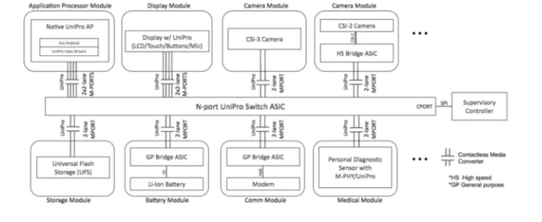
This board is the development kit for the Endoskeleton on which each module will be connected. It bridges the application processor and the modules using an UniPro
high-speed interface. The Ara team also introduced a new software protocol called Greybus, which handles the communications between the endoskeleton and the module at an
Figure 2.3: Ara Application Processor Board
higher level, making a convenient way for module developers to manipulate the UniPro
stack.
Figure 2.4: Ara Endoskeleton Switch Dev Board
2.3.6.3 GP Endpoint board
The Generic Endpoint is a development board to quickly prototype module. In fact,
it’s a kind of ”base” module on which we would be able wiring our hardware by using standard connectors and bus. The board provides a set of Input/Output such as GPIO,
Figure 2.5: Module to Module Communication (with Native UniPro Support and Bridge ASICs)
Like the AP Board, it should be connected to the Endoskeleton with 8 SMA coaxial cables.
Figure 2.6: Ara Generic Endpoint Board
2.3.6.4 MDK Configuration and Setup
State of the Art
This chapter provides an overview of the topics that supplied the ideas for this thesis.
The following sections examine the previous works which have been done on implement-ing Visible Light Communication technology.
3.1
VLC Implementations
3.1.1 Visible Light Road-to-vehicle Communication Using High-Speed Camera
LEDs are already being used in traffic lights, and they can be used as the communication
medium. Road-to vehicle communication using the LEDs in the traffic signal lights and on-vehicle high-speed camera as the receiver was proposed [11].
The bellow figure 3.1 shows the basic usage of LED as a transmitter and CAMERA as
a receiver. In this model, they mounted a camera before the front end of the car. The camera is used as the information receiver from traffic signal lights. The advantage of using the camera is that multiple data can be transmitted by the LEDs and received by
High-speed cameras.
Figure 3.1: Road-to-vehicle visible light communication
3.1.2 Integrated System of White LED Visible-Light Communication and Power-Line Communication
In [2], optical communication using the existing power-line in a household is proposed as shown in 3.2 The power-line is used for communication between white LEDs and other
fixed networks. The already installed power-lines and outlets behave as data networks and ports.
Figure 3.2: Waveform on power-line
As in optical intensity modulation, the transmitted signals are added to the cyclic
wave-form of the alternating current (AC). The transmitter signal from the PC is picked by BPF through the power-line, and biased before sending to the LED lights. The
electrical signal is then converted into an optical signal by LEDs and sends it to the photodiode, where it converts the captured optical signal to an electrical signal. The
signal is demodulated according to the received level of light and then is passed to the mobile terminal.
3.1.3 Visible Light Communication for Advanced Driver Assistant Sys-tems
Figure 3.3: General architecture for a full duplex VLC system
Optical communications for outdoor communication has been discussed and elaborated upon [4]. Devices such as laptops an mobile phones can be used for transmitting and
receiving information, using transceivers, as shown in 3.3. Transceiver systems use both LEDs and photodiodes. Intensity modulation was implemented to reach the most viable
modulation. Various important design parameters were optimized by using intensive investigation based on gain variation over 100m of transmission range [4].
3.1.4 Study of Visible Light Communication System Using RGB LED Lights
Disney research group in Zurih [12] demonstrates a half-duplex VLC LED-to-LED
com-munication with various applications with new generation toys. First example is a short-range directional communication with a number of toys, where front and backlights are
used to exchange messages when pointed towards each other. On other application is a LED light bulb in a desk lamp receiving messages from a mobile device and broadcasts
it back to the desk with higher light intensity and larger coverage. The static lamp acts as a repeater so that more devices can receive the original messages and the resulting
visible light communication
3.2.1 Visible Light Communication using smartphone camera and rolling shutter effect
Cameras embedded in smartphones can be used as VLC receivers. As a result, common
lights and smartphone cameras has the potential to enable a great number of applications with low cost. In [13], a prototype VLC system that utilizes undersampled frequency
shift ON-OFF keying (UFSOOK) modulation is proposed. The system utilizes rolling shutter cameras as the receiver and takes advantages of its characteristics to improve the
receiving performance. An LED is used as the transmitter. Information is transmitted in the continuous state (ON-OFF) changes of LEDs which are invisible to human eyes.
The performance evaluation results demonstrate that the communication prototype is robust and can resist common optical interferences and noises within the image.
3.2.2 Visible Light Communication using smartphone ambient light sensor
Other approach as been proposed using the smartphone ambient light sensor as receiver.
A light sensor is one of the most common sensors in smartphones, and is located on it’s surface above the screen. Since the screen of a smartphone is a major factor in draining
its battery, an ambient light sensor is used to recognize the brightness of its surroundings and adapt the screen backlight to save battery power while optimizing the visibility.
Some researches leverage this sensor for indoor localization or secure authentication purpose. The It’s the case of FIRE system presented in [14]. FIRE takes advantage
of a smartphone’s ambient light sensor and uses a challenge-based programmable light-emitting token generator. They have designed and prototyped an inexpensive passcode
encoder and LED light-emitting hardware. Their experiments validated that FIRE can authenticate a user on a smartphone building a bi-directional communication channel
based VLC.
4.1
System Description
Considering previous results and solutions, we propose an innovative solution, taking advantage of the Ara modular smartphone, to design a well suited front-end receiver for
visible light communication.
As the Ara platform let use choose our own hardware and receiver, we would avoid
problems and sampling limitations related to camera, or ambient light sensor. On other hand, the modular platform, through its UniPro interface on the endoskeleton board,
give us the possibility to connect our module with the same performance than if it has been directly plugged in the main application processor board. In this way, we don’t
need to use a smartphone peripheral, such as USB, or Bluetooth controller, that would add a huge overhead in the transmission and processing.
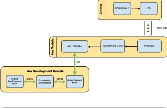
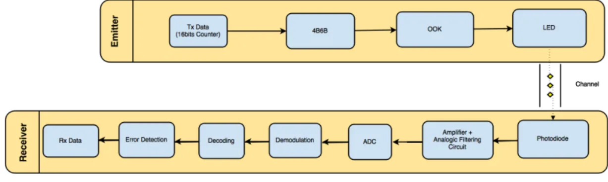
The system, that we develop as part of this project consist in a commercial LED emitter, driven by a STM32L0 micro-controller unit, in order to transmit the OOK modulated
signal. Before that, we propose to encode data using 4B6B or Manchester, in order to perform different experimentation and compare the result.
Considering the receiver module, our light sensor consist in a photodiode followed by several electronic circuit : current to tension converter, low-pass filter and positive gain
amplifier.
The analog to digital conversion has been realized at 1,1 MSPS by the micro-controller
unit. To fit the platform requirement and optimize the throughput, it performs several operations such as thresholding, decoding and buffering.
The transmission between the MCU and the Ara Development Kit is achieved through I2C bus in ”slave-transmit” mode, with the MCU as slave-node and the Ara as
master-node.
Finally, we develop a basic Android application for the platform, that implement I2C
bus initialization, data polling, and logging for later computation and analysis.
Figure 4.1: Proposal hardware implementation
4.2
VLC Contribution
Our approach would demonstrate a new VLC usage and possibility carrying an improved
among of data the the user smartphone. Even if we follow IEEE 802.15.7 standard recommendation for PHY mode, we propose to combine OOK modulation with 4B6B
Project Description
5.1
Ara platform study
In this section, we will describe different studies and preliminary experimentation we’ve done before designing the module.
In fact, because of the lake of literature or past experience with the Ara platform, we first need to study the Ara Module Development Kit send by Google ATAP. Our point
of interest was understanding the role of each board, and there I/O - regarding protocols and speed. Then we determined the reliable rate on which one the operating system
can execute a single task - such as performing an I2C operation. Finally we did some
benchmark and CPU load tests.
5.1.1 MDK and boards study
5.1.2 Android for Ara reliable I/O operation rate
5.1.2.1 Problematic
In this part, we would determine the I/O performance between the Ara main board and
modules in order to fit its characteristics: maximum ADC sampling rate, resolution, buffering needs.
application displays two graphs corresponding to the measured LED reflection at two
different frequencies.
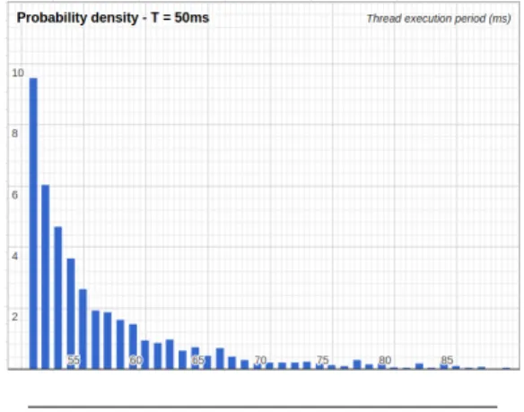
We modify the oxymeter application changing the thread execution interval from 1ms to
100ms and record the effective execution period using time-stamps. To have a consistent dataset, we record 1 million of samples for each measure. As consequence, we would be
able to determine the minimum thread execution period, and its stability. This point is particularly important for designing the buffer on the VLC receiver : a bigger I/O
operation period than expected will cause overflow, and data loss.
To determine the bus speed and the max effective transferred without error for each
operation, we replaced the oxymeter module by an Arduino that will write different among of data on the bus. In addition, we use a logic analyzer to record what’s happening
on the bus.
5.1.2.3 Results
Figure 5.1: Probability density of Android thread execution interval
with 20ms as defined period
Figure 5.2: Probability density of Android thread execution interval
Remark : as value lower than expected have no consequence, we don’t plot them on the chart, but are taken in account in the probability repartitions.
• Android threads can’t reach lower period than 8ms but with an elevate variance.
• Performing statistical analysis, for each execution period and plotting the effective
period distribution and variance, we can consider 30ms as safe.
• Even if the I2C bus speed clock rate should be 400kHz - according to the Ara
MDK documentation - the effective clock rate is 133kHz. On other hand, even if the kernel driver limits I/O operations to 512 bytes, the bus gets corrupted trying
to transfer more than 350 bytes per operation.
5.1.2.4 Conclusion
According to 5.1.2, we should design our VLC receiver module to taking account an
effective bit-rate of 92,4 kbps and will developed the Android application with a module polling thread period to 30ms and an I2C transaction .
5.1.3 Ara benchmark
In addition to 5.1.2, we should be sure that a normal to extensive modular smartphone won’t affect VLC module performances, even if the application run in background mode.
In this case, the Android CPU governor will reduce the priority of our application, giving it less resources or stopping it if necessary.
In order to do that, we use a benchmark application that would simulate typical smart-phone use-case : web browsing, short-message writing, video playing or games.
During the stress tests, both CPU load, CPU allocation, and RAM usage are monitored.
For each case, except the video game that made freeze and crash the Ara platform,
results where exactly the same than with a single activity ie. just our application -and we achieve the same bit-rate.
Figure 5.3: CPU load and allocation with only Oxymeter application running. Pro-cess on the left are system thread.
Figure 5.4: CPU load and allocation during the web browsing simulation
5.1.3.1 Conclusion
Following conclusion in5.1.2, we are now able to determine the analogical to digital
con-verter characteristic. In order to get the better ratio as possible between the resolution, the ADC sampling rate and the LED driver clock rate, we chose values summarized in
the next table.
Sampling Rate ≈1 MSPS
Resolution 8-12 bits
Buffer Size 200 bytes
5.2
Receiver circuit design
In this section, we will focus on the VLC module hardware design, that will have a major impact in the quality and efficiency of our system. Main difficulty we have to face here,
is to select appropriate circuit pattern, filters type and cute-off frequency, according to the channel characteristic. The method we applied was in a first to study the channel principal characteristic, to design a first circuit, then compute theoretical values, and
finally adjust them after some practical results.
5.2.1 Needs description
The VLC receiver front-end circuit must detect with high frequency precision the
modu-lated light within a range starting from 1kHz to MHz. Before digitalization, the current generated by the photodiode has to be converted into current. As a major issue in VLC
are interferences - from the ambient light or UV from the sun - the signal should be properly filtered and amplified before digitalization.
Our solution is constituted with a photodiode, witch convert the modulate light into
current. It’s followed by a trans-impedance amplifier in order to convert the photodiode output current into tension. Then, an analogical low-pass filter and gain are applied, before digitalization by the a micro-controller unit.
5.2.2 1st Op-Amp : Trans-Impedance Amplifier
The first part of the circuit is the Trans-Impedance Amplifier, presented in 5.5. TIA is a standard electronic pattern made from an operational amplifier and a resistor to
convert the current to a tension.
We choose the MCP6292 Op-Amp for its 10 MHz wide band pass, and 3.3V input voltage. Indeed, the interesting input frequency from modulated light won’t be greater
than 1 MHz and we will be able supply it with the MCU. The DC output voltage due to the photodiode is given by 5.1
Figure 5.5: Trans-Impedance Amplifier
The capacitance in the feed-back loop is determined to compensate the photodiode
capacitance in order to assure the operational amplifier stability which depends on C1,
R1 and CD1.
5.2.3 2nd: High Pass filter
After the Trans-Impedance Amplifier circuit part, we add a high-pass (figure 5.6 filter to attenuate the noise from the ambient lights such as sunlight and 50-120 kHz indoor
fluorescent lights.
To perform, the filter was designed with a cut-off frequency of 200 Hz. We chose C3
and R2 value. According to figure 5.7 and equation 5.2, we use 10 nF capacitance and
48 kHΩ resistor
fcf = 1
2πRC (5.2)
5.2.4 Gain
The output gain in the second part of the circuit aims to increase the signal amplitude,
without increasing the noise. As a result, we will get better SN R, and digital signal
processing and thresholding will be more accurate.
As for the TIA, a capacitance C3 of 6.8pF has been added to assure the Op-Amp
Figure 5.6: High-Pass Filter
Figure 5.7: High-Pass Filter Bode Plot
The gain GOU T has been adjusted during our final experiments with the modulated
LED and its value is given by 5.3
GOU T =
R4
R5
(5.3)
5.3
Emitter driver
In this section, we will discuss the LED emitter and driver we developed for our system.
A commercial LED has been used as a modulated light source with an on-off signal gen-erated by a micro-controller unit, that carry transmitted data encoded using a modified
Figure 5.8: Gain Operational Amplifier
5.3.1 Micro-Controller Unit
The MCU used for the LED driver is an STM32L0, exactly the same as for the receiver, because its development kit is low cost, and toolchain with software development
envi-ronment can be shared. We exploited its 3.3V digital output to blink the emitter white LED.
5.3.2 OOK modulation
Following IEEE 802.15.7 recommendations, we propose to use an On-Off Keying modu-lated signal as described in section 2.2.1 meaning that each bit 1 is mapped onto an high
output level, and bit 0 mapped onto null output on the digital micro-controller output.
5.3.3 4B6B Line coding
The line code used is a modified version of the standard 4B6B described in 2.2.3 to
increase the transmitted power. 4 bits are mapped into 6 bits always using 4 bit 1 and 2 bit 0. In that way, duty cycle is 2/3 instead of 1/2 for the standard version. This
modified version would be used as error detection too.
To compare the performance between different RLL coding, Manchester has been im-plemented to, and both coding schema can be easily switched programmatically using a
4 bits 6 bits 0000 001111 0001 010111 0010 011011 0011 011110 0100 011110 0101 100111 0110 101011 0111 101101 1000 101110 1001 101111 1010 110011 1011 110101 1100 110110 1101 111001 1110 111010 1111 111100 Table 5.2: Modified 4B6B 5.3.4 Transmission Pattern
We propose a transmission pattern that would easily allow clock synchronization on the receiver. In addition, it has been designed taking account of the flickering and dimming
issue.
Three transmissions state are defined :
• Idle : no data are transmitted, but we keep transmitting continuously111000and
000111 4B6B symbols.
• Preamble : just before sending the data, the emitter should send a preamble, to
let the receiver synchronizing. Symbols used should be different than these used
to encode the data. We propose a combination of 110100 and 001011.
• Data : 4B6B encoded data.
The table 5.3 shows the transmission of the number 2, 16 bits encoded : 0000 0000
sending periodically - or using the development board button to random timing - the
increased value, as defined in algorithm 1.
Algorithm 1 VLC Emitter main loop
time⇐O counter⇐O
while 1 do
if time≥25 then send preamble;
send 4B6B counter value;
counter ⇐counter+ 1 else send idle; end if time⇐time+ 1 end while
5.4
Receiver ADC and Buffer
In this section, we will describe the digitalization and digital processing performed by the VLC receiver module, just after the front-end circuit.
5.4.1 Hardware choice
According to 5.1, we chose to use the STM32L0 micro-controller based on an ARM Cortex M0+ processor with these characteristics :
• Processor Frequency up to 32 MHz: it will let us embedded some signal processing
• Low power consumption : 87 µA/MHz: it’s a key feature for the mobile battery powered.
• Analogical Input with 1.1 MSPS ADC : it fits our requirements.
• Different I/O, including I2C : it’s a requirement to connect the MCU to the MDK
endpoint board.
• 8kB RAM : this feature will let us implements the buffering using volatile memory
(RAM).
5.4.2 Software implementation
We developed the MCU software in C, using the Arm GCC tool-chain and ST-Link debugger interface included in the Em::Blocks IDE [15].
The MCU is initialized setting the HSI as source clock with 32MHZ as processor
fre-quency. Only I2C, UART, ADC are enabled.
The main program works in interrupt mode.
5.4.2.1 Data Acquisition
The ADC sampling rate is set to 1,1 MSPS, in order to get the higher frequency precision,
and the resolution to 8 bits, enough for OOK modulation.
The acquisition is done using buffering and Direct Memory Access (DMA) mode. When
the DMA buffer is full, an interruption is thrown starting the demodulation and RLL decoding process.
5.4.2.2 Demodulation and RLL Decoding
First step is the the OOK demodulation that consisting in applying a threshold to the value.
1 u i n t 8 _ t A R A _ A D C _ T h r e a s h o l d(u i n t 3 2 _ t v o l t a g e)
2 {
5.4.2.3 Buffering
After being decoded , bits are pushed into a FIFO Buffer implemented in D
1 t y p e d e f s t r u c t 2 { 3 u i n t 8 _ t *b u f p t r; // p o i n t e r to the b u f f e r a r r a y 4 s i z e _ t b u f s i z e; // s i z e of b u f f e r 5 s i z e _ t r d i d x; // p o i n t s to n e x t a d d r e s s to be r e a d 6 s i z e _ t w r i d x; // p o i n t s to n e x t a d d r e s s to be w r i t t e n 7 # if( F I F O _ L O G _ M A X _ U S A G E == 1) 8 s i z e _ t max; 9 # e n d i f 10 } F I F O _ t; Listing 5.2: fifo.h 5.4.2.4 Input/output
1. UART peripheral is enabled only in debugging case or to record measures to the
laptop via Serial-to-USB port.
2. I2C is enabled in slave mode and connected to the Ara module development board.
An interruption is thrown when a read request coming from the master peripheral driven by the Android application. is detected
The function called in the interruption callback flush the last 350 bytes, to send
them to the I2c.
1 v o i d H A L _ I 2 C _ S l a v e T x C p l t C a l l b a c k (I 2 C _ H a n d l e T y p e D e f *I 2 C x H a n d l e)
3 F l u s h _ B u f f e r((u i n t 8 _ t*)a T x B u f f e r, a T x S i z e) ;
4 R E S _ t res = F I F O _ r e a d(&AdcFIFO, &a T x B u f f e r, a T x S i z e) ;
5 }
Listing 5.3: I2c interrupt Callback
5.5
Ara Android App
In this part, we describe the Android application that we have developed, to support our VLC receiver module.
5.5.1 Application structure and operations
Our application as been developed using Android Studio IDE [16] with the Gradle build toolchain. The target SDK API version is number 18, to be compliant with the operating
system version which has been installed on the AP Development Board.
The application package has been called respecting Java name convention :
1 p a c k a g e edu.upc.e n t e l.wng.v l c A r a M o d u l e;
This package includes 3 classes :
• VLCAraActivity : initialize the application and user interface. It surcharges the
Activity class , as requested by the Android API.
• Sensor : define and perform operations to communicate with our module such as
I2C bus initialization, data polling as well as handling and message with the User
Interface (UI).
• VlcLogger : this class realize logging operation saving received data on the board
internal storage or an external SD Card.
Application workflow is quiet simple :
5.5.2 User Interface
The application user interface as few components as defined in the XML activity layout
description file :
• EditText field: used to display received bits.
• ”Clear” and ”Save” Button :
Each component are placed in a horizontal layout container.
Figure 5.9: Android application receiving data via VLC
5.5.3 I2C JNI interface
As the Android Java API for the Ara Module Development Kit is the same as the standard API, we need to implement additional components in order to access the low
level hardware such as the GPIO or the I2C bus. The Ara MDK is provided with an
operating system level driver, developed in C, that can be used to configure, read and
the Java API. In order to give the possibility to perform I2C operations in our Android application, we develop a JNI interface that would wrap the C driver into a Java package.
So we define 2 Java classes :
• I2CManager : it configures the I2C bus, by using UNIX I2C kernel driver and
execute operations defined in I2CTransaction.
• I2CTransaction : it represents read or write operation on the bus.
6.1
Experimental setup
We propose to evaluate different aspects and characteristics of our system considering an indoor communication situation avoiding sunlight perturbations.
In addition, we consider different cases: with or without ambient light interferences, Manchester or 4B6B coding, changing the clock rate and the emitter distance from the
receiver.
6.2
Protocol
The receiver was placed in a fix position, while the LED light source keep mobile. In
that way, the distance between the emitter and the receiver can be changed. To keep the measure consistent, we place a luxmeter, just near the receiver to approximate the
effective illumination.
During the probes, both emitter and receiver micro-controller were connected with their debugging interface to a laptop, on a side to change the LED driver parameters, and on other side to visualize and record received data at different place of our system.
In addition, we used on oscilloscope to check the circuit output and control the signal generated by the emitter micro-controller.
The emitter light was alimented with a 28 Volts power supply and the LED Driver has been programmed to send periodically a 16-bits counter value, with the pattern defined
in 5.3.4.
About the distance/illumination, probes have been realized in a range of 75 to 300
centimeters to match an indoor possible usage. On other side, the clock frequency
has been limited to 560kHz, considering the ADC sampling rate - 1,1 MSPS - and the
Nyquist-Shannon sampling theorem :
fN yquist =
fsampling
2 (6.1)
Figure 6.1: The Ara MDK and its VLC receiver module
6.3
Circuit Evaluation
The received signal was measured at different steps of the analogical processing, using
the 2 oscilloscope voices at different points of our circuit. The high-pass filter and
adjustments made on the receiver front-end circuit are satisfactory, and improve the
signal quality before sampling.
Figure 6.2: Receiver illumination over the distance
Figure 6.3: In yellow the signal just after the TIA. In blue, the signal after analogical filtering - 2,5 meter distance
In order evaluate our demodulation and digital processing algorithms, we plot the sam-pled signal and the bits obtained after computation. We can see in the figure 6.4 that
it is correct and we can get rid of signal attenuation due to circuit latency.
6.4
Bit Error Rate
In digital transmission, the number of bit errors is the number of received bits of a data stream over a communication channel that have been altered due to noise, interference,
Figure 6.4: In red the signal sampled. In blue, the bits computed after digital pro-cessing and demodulation
As we know exactly the sequence of bit that have been emitted and the decoded
se-quence, we were able to compute it, for different illumination level and clock-rate, using Manchester or 4B6B coding.
6.4.1 4B6B
clock rate (kHz) bitrate (kbps) BER
100 67 <10−4
160 107 <10−4
240 160 3.10−4
380 253 6.10−4
560 373 2.10−2
Table 6.1: Bit Error Rate for different clock rate at 2,5 meters, using 4B6B coding
Considering table 6.1 2,5 meters distance and 10−3 as admissible BER, we can assume
that using a 380kHz clock rate can be used for a correct transmission using 4B6B.
In that case, with 4B6B coding, we obtain a raw throughput of 253 kbps.
6.4.2 Manchester
Using Manchester coding, we obtained a surge of the bit error rate when the illumination is lower than 100 Lux. Analyzing the signal at the ADC input, we put in evidence that
this is due to wave attenuation : isolated bit, just after long sequences are not detected, as visible in the figure 6.5.
Figure 6.5: In blue, the signal generated by the LED driver. In yellow, the signal after our circuit - 2,5 meter distance - 360kHz
6.5
Discussion
Regarding previous results, we were able to validate our proposal. We can achieve a reliable transmission between a commercial LED and the modular smartphone at a
suitable distance for indoor usage.
Comparing our module for Ara platform with previous system, such [17], or other pro-posal using the smartphone camera and rolling shutter effect [13], we obtained and
Conclusion
7.1
Achieved work
In this project, we demonstrate the new opportunity and usage that the recent concept of modular smartphone and Ara platform give to the smartphone, extending its hardware
to support visible light communication.
We finally develop a VLC receiver module for the Ara smartphone using the development
kit provided by Google, with the full communication chain - including the emitter LED driver - in order to test it.
In this way, we were able to give our contribution to the VLC research, probing a modified version of 4B6B runlength-limited coding associated with the On-Off Keying modulation.
Bringing a suitable and dedicated receiver to the smartphone, we overcome past results in term of bitrate, in an indoor transmission scenario, between a lightening LED and a
smartphone.
7.2
Future works
On the one hand, regarding our work and results, we might improve them in different ways. First the circuit need a better expertise to increase it’s stability, or interferences
tolerance, and obtain a better SNR ratio. Then, the release of the MDK v0.2 and the
smartphone, open the door to further modules development to bring M2M and IoT
[1] Xiaohan Liu, H. Makino, and Y. Maeda. Basic study on indoor location estimation
using visible light communication platform. InEngineering in Medicine and Biology
Society, 2008. EMBS 2008. 30th Annual International Conference of the IEEE, pages 2377–2380, Aug 2008. doi: 10.1109/IEMBS.2008.4649677.
[2] Honglei Li, Xiongbin Chen, Junqing Guo, Zongyu Gao, and Hongda Chen. An
analog modulator for 460 mb/s visible light data transmission based on ook-nrs
modulation.Wireless Communications, IEEE, 22(2):68–73, April 2015. ISSN
1536-1284. doi: 10.1109/MWC.2015.7096287.
[3] Xiaoxue Ma, Kyujin Lee, and Kyesan Lee. Appropriate modulation scheme for
visible light communication systems considering illumination. Electronics Letters,
48(18):1137–1139, August 2012. ISSN 0013-5194. doi: 10.1049/el.2012.2195.
[4] Jin-Yuan Wang, Jun-Bo Wang, Ming Chen, and Xiaoyu Song. Dimming scheme
analysis for pulse amplitude modulated visible light communications. In Wireless
Communications Signal Processing (WCSP), 2013 International Conference on, pages 1–6, Oct 2013. doi: 10.1109/WCSP.2013.6677037.
[5] S.E. Alavi, H. Rezaie, and A.S.M. Supa’at. Application of ofdm on integrated
system of visible free space optic with plc. InApplied Electromagnetics (APACE),
2010 IEEE Asia-Pacific Conference on, pages 1–5, Nov 2010. doi: 10.1109/APACE. 2010.5720114.
[6] S. Rajagopal, R.D. Roberts, and Sang-Kyu Lim. Ieee 802.15.7 visible light
com-munication: modulation schemes and dimming support. Communications
Maga-zine, IEEE, 50(3):72–82, March 2012. ISSN 0163-6804. doi: 10.1109/MCOM.2012. 6163585.
pages 57–61, May 2014. doi: 10.1109/DAAS.2014.6842427.
[9] Nam-Tuan Le, Trang Nguyen, and Yeong Min Jang. Frequency shift on-off keying
for optical camera communication. In Ubiquitous and Future Networks (ICUFN),
2014 Sixth International Conf on, pages 22–25, July 2014. doi: 10.1109/ICUFN. 2014.6876741.
[10] S. Schmid, G. Corbellini, S. Mangold, and T.R. Gross. An led-to-led
visi-ble light communication system with software-based synchronization. In
Globe-com Workshops (GC Wkshps), 2012 IEEE, pages 1264–1268, Dec 2012. doi: 10.1109/GLOCOMW.2012.6477763.
[11] M. Wada, T. Yendo, T. Fujii, and M. Tanimoto. Road-to-vehicle communication
using led traffic light. InIntelligent Vehicles Symposium, 2005. Proceedings. IEEE,
pages 601–606, June 2005. doi: 10.1109/IVS.2005.1505169.
[12] S. Schmid, G. Corbellini, S. Mangold, and T.R. Gross. An led-to-led
visi-ble light communication system with software-based synchronization. In
Globe-com Workshops (GC Wkshps), 2012 IEEE, pages 1264–1268, Dec 2012. doi: 10.1109/GLOCOMW.2012.6477763.
[13] Peng Ji, Hsin-Mu Tsai, Chao Wang, and Fuqiang Liu. Vehicular visible light
communications with led taillight and rolling shutter camera. In Vehicular
Tech-nology Conference (VTC Spring), 2014 IEEE 79th, pages 1–6, May 2014. doi: 10.1109/VTCSpring.2014.7023142.
[14] K. Dhondge, Baek-Young Choi, Sejun Song, and Hyungbae Park. Optical wireless
authentication for smart devices using an onboard ambient light sensor. In
Com-puter Communication and Networks (ICCCN), 2014 23rd International Conference
[15] Em::Blocks. Em::blocks ide, March 2015. URL http://www.emblocks.org.
[16] Google Android. Android studio ide, March 2015.
[17] E. Sarbazi and M. Uysal. Phy layer performance evaluation of the ieee 802.15.7
vis-ible light communication standard. InOptical Wireless Communications (IWOW),
2013 2nd International Workshop on, pages 35–39, Oct 2013. doi: 10.1109/IWOW. 2013.6777772.
The ARA development kit is shipped with 3 components : ● Ara Development Board (rev. D) : that’s the main board, embedding an ARMv7l processor, SD Card with a custom Android Operating System (v4.3) ● Generic Endpoint : it provides GPIO connectivity ● Endo Dev Board Dev Board assembly and wiring Endo Switch CH6 > GPIO Extension Board Endo Switch CH4 > AP Android Board Tx > Rx N > N and CLK_N > CLK_N P > P and CLK_P > CLK_P Pulse Oxymeter From left (purple) to right (black), the connections : SCL, SDA, Power (3V3) and Ground.
Power Sequence 1 Switch on the Endo Switch Board 2 Wait at least 15 seconds (to allow the switch to boot) 3 Switch on the GP Endpoint Board 4 Wait a few seconds for UniPro linkup 5 Switch on the AP Board Shutdown 1 Power Off Android. Press during 34 seconds. 2 Once Android is down, no order importance.
Additional LCD Screen Moto X on the DSI port. Speed Modulation, Byte Rate and Framing ● system rate: 20000 micro seconds = (https://aramdk.googlesource.com/platform/frameworks/base/+/master/ core/java/android/hardware/SensorManager.java#624) ● on the app : 20 ms => 50hz
● TI AFE4400 : Analogic frontend for PulseOx http://www.ti.com/product/afe4400 ➔ 4 Mhz clock ➔ PRP Count Pulse repetition period count Can be set from 800 to 64000. Set by the Android app to 7999. ➔ Max sampling rate = 1,3 KSPS ➔ Default sampling rate = 500 SPS ➔ Max résolution = 22 Bits ● IS602B : I2C to SPI http://www.nxp.com/products/interface_and_connectivity/bridges/i2c_slave_to_s pi_master_gpio_bridges/SC18IS602BIPW.html ➔ supports I²C data transfers up to 400 kHz. ➔ SPI master operating up to 1.8 Mbit/s ➔ 200byte data buffer
Circuit Schematics
Figure B.1: VLC Receiver front-end circuit
2 * * * * * * * * * * * * * * * * * * * * * * * * * * * * * * * * * * * * * * * * * * * * * * * * * * * * * * * * * * * * * * * * * * * * * * * * * * * * * * 3 * @ f i l e Src / m a i n . c 4 * @ a u t h o r A l e x i s D u q u e 5 * @ v e r s i o n V0 . 0 .1 6 * @ d a t e 30 - Avril - 2 0 1 5 7 * @ b r i e f VLC E m i t t e r D r i v e r 8 * * * * * * * * * * * * * * * * * * * * * * * * * * * * * * * * * * * * * * * * * * * * * * * * * * * * * * * * * * * * * * * * * * * * * * * * * * * * * * 9 */ 10 11 /* I n c l u d e s - - - */ 12 # i n c l u d e " m a i n . h " 13 # i n c l u d e " 4 b6b . h " 14 # i n c l u d e " s t m 3 2 l 0 x x _ i t . h " 15 16 /* P r i v a t e t y p e d e f - - - */ 17 /* P r i v a t e d e f i n e - - - */ 18 # d e f i n e B I T _ P E R I O D 1 19 // # d e f i n e C O D E _ 4 B 6 B 56
20 /* P r i v a t e m a c r o - - - */ 21 /* P r i v a t e v a r i a b l e s - - - */ 22 /* P r i v a t e v a r i a b l e s - - - */ 23 U A R T _ H a n d l e T y p e D e f h u a r t 2; 24 25 u i n t 8 _ t a R x B u f f e r[R X B U F F E R S I Z E]; 26 u i n t 8 _ t m e s s a g e[] = " 1 1 0 1 1 1 0 1 "; 27 u i n t 1 6 _ t c o u n t e r = 0; 28 int i = 0; 29 /* P r i v a t e f u n c t i o n p r o t o t y p e s - - - */ 30 v o i d S y s t e m C l o c k _ C o n f i g(v o i d) ; 31 v o i d G P I O _ I n i t() ; 32 v o i d s e n d M a n c h e s t e r M e s s a g e(v o i d) ; 33 v o i d s e n d M a n c h e s t e r C o u n t e r(v o i d) ; 34 v o i d s e n d 4 B 6 B C o u n t e r() ; 35 v o i d s e n d 4 B 6 B E n c o d e d 6 B i t s(u i n t 8 _ t b i t s) ; 36 v o i d s e n d M a n c h e s t e r D e f a u l t M e s s a g e(v o i d) ; 37 v o i d s e n d P r e a m b u l e(v o i d) ; 38 v o i d s e n d S t a r t B i t(v o i d) ; 39 v o i d s e n d S t o p B i t(v o i d) ; 40 v o i d s e n d N o D a t a(v o i d) ; 41 v o i d d e l a y (int a) ; 42 v o i d s e n d 0(v o i d) ; 43 v o i d s e n d 1(v o i d) ; 44 l o n g t i m e = 0; 45 // v o i d U S A R T 2 _ U A R T _ I n i t () ; 46 47 G P I O _ I n i t T y p e D e f G P I O _ I n i t S t r u c t; 48 49 int m a i n(v o i d) 50 { 51 H A L _ I n i t() ; 52 S y s t e m C l o c k _ C o n f i g() ; 53 S y s T i c k _ I n i t() ; 54 G P I O _ I n i t() ; 55 // U S A R T 2 _ U A R T _ I n i t () ; 56 B S P _ P B _ I n i t(B U T T O N _ K E Y, B U T T O N _ M O D E _ E X T I) ;
66 c o u n t e r++; 67 t i m e = 0; 68 } 69 e l s e 70 { 71 s e n d N o D a t a() ; 72 } 73 74 } 75 } 76 77 78 /* * 79 * @ b r i e f EX T I l i n e d e t e c t i o n c a l l b a c k . 80 * @ p a r a m G P I O _ P i n : S p e c i f i e s the p i n s c o n n e c t e d E X T I l i n e 81 * @ r e t v a l N o n e 82 */ 83 v o i d H A L _ G P I O _ E X T I _ C a l l b a c k(u i n t 1 6 _ t G P I O _ P i n) 84 85 86 { 87 if(G P I O _ P i n == K E Y _ B U T T O N _ P I N) 88 { 89 s e n d P r e a m b u l e() ; 90 s e n d S t a r t B i t() ; 91 # i f n d e f C O D E _ 4 B 6 B 92 s e n d M a n c h e s t e r D e f a u l t M e s s a g e() ; 93 // s e n d M a n c h e s t e r C o u n t e r () ; 94 # e l s e 95 s e n d 4 B 6 B C o u n t e r() ; 96 # e n d i f 97 s e n d S t o p B i t() ;
98 c o u n t e r++; 99 } 100 101 } 102 103 v o i d d e l a y (int a) 104 { 105 v o l a t i l e int i,j; 106 107 for (i=0 ; i < a ; i++) 108 { 109 j++; 110 } 111 112 r e t u r n; 113 } 114 115 /* * C o n f i g u r e p i n s as 116 * A n a l o g 117 * I n p u t 118 * O u t p u t 119 * E V E N T _ O U T 120 * E X T I 121 */ 122 v o i d G P I O _ I n i t(v o i d) 123 { 124 125 G P I O _ I n i t T y p e D e f G P I O _ I n i t S t r u c t; 126 127 /* G P I O P o r t s C l o c k E n a b l e */ 128 _ _ G P I O C _ C L K _ E N A B L E() ; 129 _ _ G P I O H _ C L K _ E N A B L E() ; 130 _ _ G P I O A _ C L K _ E N A B L E() ; 131 132 /* C o n f i g u r e G P I O pin : P C 1 3 */ 133 G P I O _ I n i t S t r u c t.Pin = G P I O _ P I N _ 1 3; 134 G P I O _ I n i t S t r u c t.M o d e = G P I O _ M O D E _ E V T _ R I S I N G; 135 G P I O _ I n i t S t r u c t.P u l l = G P I O _ N O P U L L; 136 H A L _ G P I O _ I n i t(GPIOC, &G P I O _ I n i t S t r u c t) ; 137 138 /* -2 - C o n f i g u r e PA .5 IO in o u t p u t push - p u l l m o d e to
148 v o i d s e n d P r e a m b u l e(v o i d) 149 { 150 s e n d 1() ; 151 s e n d 1() ; 152 s e n d 0() ; 153 s e n d 1() ; 154 s e n d 0() ; 155 s e n d 0() ; 156 157 s e n d 0() ; 158 s e n d 0() ; 159 s e n d 1() ; 160 s e n d 0() ; 161 s e n d 1() ; 162 s e n d 1() ; 163 } 164 165 v o i d s e n d S t a r t B i t(v o i d) 166 { 167 s e n d 0() ; 168 } 169 170 v o i d s e n d S t o p B i t(v o i d) 171 { 172 s e n d 0() ; 173 s e n d 0() ; 174 s e n d 1() ; 175 s e n d 0() ; 176 s e n d 1() ; 177 s e n d 1() ; 178 } 179
180 v o i d s e n d M a n c h e s t e r D e f a u l t M e s s a g e(v o i d) 181 { 182 s e n d 1() ; 183 s e n d 0() ; 184 s e n d 1() ; 185 s e n d 0() ; 186 s e n d 0() ; 187 s e n d 1() ; 188 s e n d 1() ; 189 s e n d 0() ; 190 s e n d 1() ; 191 s e n d 0() ; 192 s e n d 1() ; 193 s e n d 0() ; 194 s e n d 0() ; 195 s e n d 1() ; 196 s e n d 1() ; 197 s e n d 0() ; 198 } 199 200 v o i d s e n d M a n c h e s t e r M e s s a g e() 201 { 202 for(i=0; i<s i z e o f(m e s s a g e) ; i++) 203 { 204 s w i t c h(m e s s a g e[i]) 205 { 206 c a s e 0: 207 s e n d 0() ; 208 s e n d 1() ; 209 b r e a k; 210 211 c a s e 1: 212 s e n d 1() ; 213 s e n d 0() ; 214 b r e a k; 215 216 d e f a u l t: 217 b r e a k; 218 } 219 } 220 }