City, University of London Institutional Repository
Citation: Karim, Mohammad (2015). Design and optimization of chalcogenide
waveguides for supercontinuum generation. (Unpublished Doctoral thesis, City University London)
This is the accepted version of the paper.
This version of the publication may differ from the final published version.
Permanent repository link: http://openaccess.city.ac.uk/13592/
Link to published version:
Copyright and reuse: City Research Online aims to make research outputs of City, University of London available to a wider audience. Copyright and Moral Rights remain with the author(s) and/or copyright holders. URLs from City Research Online may be freely distributed and linked to.
City Research Online: http://openaccess.city.ac.uk/ [email protected]
waveguides for supercontinuum
generation
Mohammad Rezaul Karim
School of Mathematics, Computer Science and Engineering City University London
This dissertation is submitted for the degree of
Doctor of Philosophy
I hereby declare that except where specific reference is made to the work of others, the contents of this dissertation are original and have not been submitted in whole or in part for consideration for any other degree or qualification in this, or any other university. I grant powers of discretion to the University Librarian to allow this thesis to be copied in whole or in part without further reference to me. This permission covers only single copies made for study purposes, subject to normal conditions of acknowledgement.
Firstly, I would like to thank my supervisor Prof. B M A Rahman for guidance and support during the last three years. His help was invaluable to me during the whole course of research work on chalcogenide waveguides for supercontinuum generation.
Next, I would like to thank all the professional people I become acquainted with during the last three years. Particularly, I am grateful to Prof. Govind P. Agrawal who helped me a lot during his visit to City University London with discussion on various nonlinear effects and resolving different problems arises during numerical simulations on SC generation.
I would like to thank all of my colleagues in the Photonics Modelling Research group for all the help and contributions they have provided me during the three-year course of research work. I express my thanks to the all academic and administration staffs of City University London for conducting and managing this process very smoothly.
I would like to endlessly thank to my parents for guiding and encouraging me all time to keep me in the right path as well as brighten up my future. And thanks to my all other family members and relatives who have given me support in many ways during this course of study.
This research work presents numerical simulations of supercontinuum (SC) generation in optical waveguides based on Ge11.5As24Se64.5chalcogenide (ChG) material. Rigorous numerical simulations were performed using finite-element and split-step Fourier methods in order to optimize the waveg-uides for wideband SC generation. Through dispersion engineering and by varying dimensions of the 1.8-cm-long ChG nanowires, we have investigated dispersion curves for a number of nanowire geometries and identified a promising one which can be used for generating a SC with 1300 nm bandwidth pumped at 1550 nm with a low peak power of 25 W. It was observed through successive inclusion of higher-order dispersion coefficients during SC simulations that there is a possibility of obtaining spurious results if the adequate number of dispersion coefficients is not considered. We then investigate MIR SC in dispersion-tailored, air-clad, ChG channel waveguide employing either Ge11.5As24S64.5or MgF2glass and ChG rib waveguide employing MgF2glass for their lower claddings. We study the effect of waveguide parameters on the bandwidth of the SC at the output of 1-cm-long waveguides. Our results show that output can vary over a wide range depending on their design and the pump wavelength employed. At the pump wavelength of 2µm the SC never extended beyond 4.5µm for any of our designs. However, SC could be extended to beyond 5µm for a pump wavelength of 3.1µm. A broadband SC spanning from 2 to 6µm and extending over 1.5 octave could be generated with a moderate peak power of 500 W at a pump wavelength of 3.1
µm using an air-clad, all-ChG, channel waveguide. We show that SC can be extended even further covering the wavelength ranges 1.8-7.7µm and 1.8-8 µm (>2 octaves) when MgF2glass is used for the lower claddings of ChG channel waveguide and rib waveguide, respectively. By employing the same pump source, we show that SC spectra can cover a wavelength range of 1.8-11µm (>2.5 octaves) in a channel waveguide and 1.8-10µm in a rib waveguide employing MgF2glass for their lower claddings with a moderate peak power of 3 kW. Finally we present microstrucured fibre based design made with same glass to generate SC spectra in the MIR region. Numerical simulations show that such a 1-cm-long fibre can produce a spectrum extending from 1.3µm to beyond 11µm (>
List of figures xiv
List of tables xx
List of Acronyms xxi
List of Symbols xxiv
1 Indroduction 1
2 Nonlinear optics in optical waveguides 7
2.1 Light propagation in optical waveguides . . . 8
2.1.1 Maxwell’s equations . . . 8
2.1.2 Nonlinear pulse propagation equation . . . 12
2.2 Linear effects in optical waveguides . . . 15
2.2.1 Losses . . . 15
2.2.2 Dispersion . . . 16
2.3 Nonlinearity in optical waveguides . . . 18
2.3.1 Self-phase modulation . . . 20
2.3.2 Solitons . . . 21
2.3.3 Cross-phase modulation . . . 23
2.3.4 Four-wave mixing . . . 24
2.3.5 Self-steepening . . . 25
2.3.6 Stimulated Raman scattering . . . 26
2.3.7 Dispersive waves . . . 28
2.4 Summary . . . 29
3.2 Finite-element method . . . 34
3.2.1 The variational approach . . . 36
3.2.2 FE method implementation . . . 41
3.3 Split-step Fourier method . . . 54
3.3.1 SSFM for solving GNLSE . . . 54
3.3.2 SSFM implementation . . . 57
3.4 Summary . . . 58
4 Overview of SC generation 60 4.1 SC generation in bulk media . . . 61
4.2 SC generation in conventional fibres . . . 62
4.3 SC generation in silica microstructured fibres . . . 64
4.4 SC generation using nonsilica fibres . . . 66
4.5 Summary . . . 71
5 SC generation in chalcogenide nanowire 73 5.1 Material properties of ChG glasses . . . 74
5.2 ChG nanowire design . . . 77
5.2.1 Structure of ChG nanowire . . . 77
5.2.2 Aitken extrapolation technique for accuracy testing of FE modal solution . . . 78
5.2.3 Calculation of GVD and higher-order dispersions . . . 81
5.2.4 Accuracy testing of GVD with the variation of FE mesh and data fitting through Taylor series expansion . . . 84
5.3 Simulation parameters for SC generation . . . 87
5.4 Results and discussions . . . 88
5.5 Simulated SC result verification with frequency domain method . . . 97
5.6 Summary . . . 98
6 Mid-infrared SC generation in chalcogenide waveguides 100 6.1 ChG channel and rib waveguides design . . . 101
6.1.1 Geometry of channel and rib waveguides . . . 101
6.1.2 Dispersion engineering of channel waveguides . . . 102
6.1.3 Dispersion tailoring of a rib waveguide . . . 108
6.2 Simulation parameters for MIR SC modelling . . . 111
6.3.2 Simulation results for channel waveguides pump employing at 3.1µm115
6.3.3 Simulation results for a rib waveguide pump employing at 3.1µm . 119
6.4 Summary . . . 124
7 Mid-infrared SC generation in chalcogenide microstructured fibres 126 7.1 Microstructured fibres (MoFs) design . . . 128
7.1.1 Structure of MoFs . . . 128
7.1.2 Dispersion tailoring for hexagonal PCF . . . 129
7.1.3 Dispersion tailoring for TC fibre . . . 132
7.1.4 Dispersion tailoring for equiangular spiral PCF . . . 134
7.2 Simulation parameters for SC modelling in ChG MoFs . . . 138
7.3 Results and discussions . . . 139
7.3.1 SC generation in hexagonal PCF . . . 139
7.3.2 SC generation in TC fibre . . . 141
7.3.3 SC generation in ES-PCF . . . 142
7.3.4 Comparison of SC evolution in MoFs output . . . 142
7.4 Summary . . . 147
8 Conclusion and Future work 149
Appendix A 157
Appendix B 160
Author Publications 165
2.1 Normalized Raman gain for fused silica when pump and stokes wave are
copolarized (After [1]) . . . 26
3.1 Schematics of (a) planar (channel) waveguide and (b) PCF with hexagonal symmetry cladding containing air-holes. . . 32
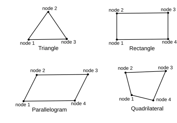
3.2 Two dimensional elements. . . 41
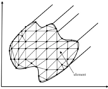
3.3 Finite element discretisation of an irregular waveguide cross-section. . . 42
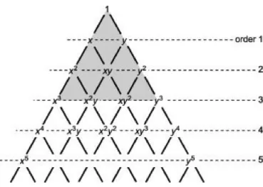
3.4 Pascal’s triangle for complete polynomials in two dimensions. . . 43
3.5 Typical two dimensional first order triangular element. . . 44
3.6 Discretisation of a dielectric waveguide with orthodox and infinite elements. 53 3.7 Schematic diagram of the symmetrized SSFM used for numerical simulations. Waveguide length is divided into a large number of segments of widthhand the effect of nonlinearity is included at the mid of the step shown by a dashed line. . . 56
5.1 Schematic diagram of chalacogenide nanowire. . . 77
5.2 Dominant Hy field profile of fundamental quasi TE-mode (H11y ) for the nanowire structure ofW = 700 nm andH = 500 nm at a wavelength of 1550 nm; a) Contour, b) Surface, c) Hyfield along width, and d) Hyfield along thickness of a nanowire. . . 79
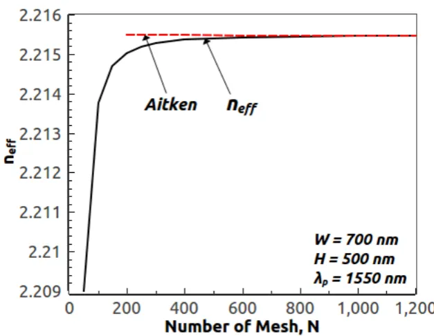
5.3 Variation ofneffof the fundamental quasi-TE mode with the mesh size and improvement realized with the Aitken extrapolation technique. . . 81
5.5 GVD for the fundamental quasi-TE mode as a function of wavelength for the naowire structure withW = 700 nm andH = 500 nm. The black-solid, red-dashed, and blue-dotted correspond to a mesh size of 200×200, 300×300, and 600×600, respectively. . . 85 5.6 GVD curves obtained with FE method (black) fitted the Taylor series
expan-sion up toβ8for the nanowires (a)W = 775 nm,H= 500 nm and (b)W =
800 nm,H= 500 nm. . . 86 5.7 Changes in SC spectra with the successive addition of higher-order dispersion
terms pumped at a wavelength of 1550 nm for the nanowire of dimensions
W = 700 nm andH = 500 nm. . . 89 5.8 Temporal intensity (top), spectral density (middle) and spectrogram (bottom)
including terms up toβ3(left column), up toβ4(middle column), and up to
β8(right column) pumped at a wavelength of 1550 nm for the nanowire of
dimensionsW= 700 nm andH= 500 nm. . . 90 5.9 Changes in SC spectra with the successive addition of higher-order dispersion
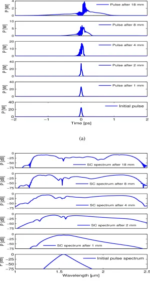
terms pumped at a wavelength of 1550 nm for the nanowire geometry,W = 775 nm andH= 500 nm. . . 92 5.10 (a) Temporal and (b) Spectral evolution for 50 fs pulse launched with 25
W peak power pumped at a wavelength of 1550 nm along the length of the nanowire structure,W = 775 nm andH = 500 nm. . . 93 5.11 Temporal intensity (top), spectral density (middle) and spectrogram (bottom)
including terms up toβ3 (left column), up toβ4(middle column), and up
toβ8(right column) pumped at a wavelength of 1550 nm for the nanowire
geometry,W = 775 nm andH = 500 nm. . . 95 5.12 Numerically simulated SC spectra for nanowires with the dispersion curves
shown in Fig. 5.4(a) by including dispersion terms up to β8 at a pump
wavelength of 1550 nm. . . 96 5.13 Numerically simulated SC spectra for nanowire, W = 775 nm and H =
500 with time domain (SSFM) and frequency domain (Interaction Picture) including dispersion terms up toβ8at a pump wavelength of 1550 nm with a
peak power of 25 W. . . 97 6.1 Schematic diagram of ChG rib waveguide. . . 102 6.2 GVD curves for the fundamental quasi-TE mode calculated fromneff for
three waveguides geometries employing As36S64glass for both the upper and
6.3 GVD curves for the waveguide geometries employing two different lower claddings (solid black curve for Ge11.5As24S64.5and red dashed curve for
MgF2) for the fundamental quasi-TE mode (a) at a pump wavelength of 2
µm and (b) at a pump wavelength of 3.1µm. Vertical dotted line indicates
the position of pump wavelength. . . 105 6.4 Dominant field profile for fundamental quasi-TE mode (H11y ) for the ChG
channel waveguide geometry, W = 4 µm and H = 1.6 µm employing
Ge11.5As24S64.5glass for its lower cladding at a wavelength of 3100 nm; a)
Contour, b) Surface, c) Hyfield along width, and d) Hyfield along thickness
of the waveguide. . . 106 6.5 Dominant field profile for fundamental quasi-TE mode (H11y ) for the channel
structure ofW = 5 µm andH = 0.95 µm employing MgF2 for its lower
cladding at a wavelength of 3100 nm; a) Contour, b) Surface, c) Hyfield
(normalized value) along width, and d) Hy field (normalized value) along
thickness of the waveguide. . . 107 6.6 Dominant field profile for fundamental quasi-TE mode (H11y ) for the rib
structure ofW = 5 µm and H = 1.1 µm employing MgF2 for its lower
cladding at a wavelength of 3100 nm; a) Contour, b) Surface, c) Hyfield
(normalized value) along width, and d) Hy field (normalized value) along
thickness of the waveguide. . . 109 6.7 GVD curve (solid red line) tailored for the fundamental quasi-TE mode
calculated from neff and dotted black line curve represents the material dispersion (DM) of Ge11.5As24Se64.5 ChG material. Vertical dotted line
indicates pump wavelength and the inset shows the spatial profile of the fundamental mode at a wavelength of 3.1µm. . . 110
6.8 Simulated SC spectra at a pump wavelength of 2 µm for (a) air-clad
all-chalcogenide waveguide at peak power from 25, 100, and 500 W; (b) air-clad chalcogenide core employing MgF2for its lower cladding at the same power
levels. . . 113 6.9 Simulated SC spectra at a pump wavelength of 2µm for waveguides with
two different lower claddings at a peak power of 500 W only. Black-solid line curve represents the SC spectrum for the waveguide containing Ge11.5As24S64.5glass for its lower cladding and red-dashed line curve
6.10 Spectral evolution at a pump wavelength of 2µm for (a) air-clad all-chalcogenide
waveguide at a peak power of 500 W; (b) air-clad chalcogenide core employ-ing MgF2for its lower cladding at the same power level. . . 115
6.11 Simulated SC spectra at a pump wavelength of 3.1 µm for (a) air-clad
all-chalcogenide waveguide at peak power between 100 W and 3000 W; (b) air-clad chalcogenide core employing MgF2for its lower cladding for the
same power levels. . . 116 6.12 Simulated SC spectra at a pump wavelength of 3.1µm for (a) waveguides
employing with two different lower claddings at a peak power of 500 W only; (b) waveguides with two different lower claddings at peak power of 3000 W only. Black-solid line curve represents the SC spectrum for the waveguide structure containing Ge11.5As24S64.5glass for its lower cladding
and red-dashed line curve represents the spectrum for the structure with MgF2as its lower cladding. . . 117
6.13 Spectral evolution along the waveguide length at a pump wavelength of 3.1µm for waveguides with (a) Ge11.5As24S64.5and (c) MgF2as its lower
claddings at a peak power of 500 W only; (b) Ge11.5As24S64.5and (d) MgF2
as its lower claddings with a peak power of 3000 W only. . . 118 6.14 Simulated SC spectra at a pump wavelength of 3.1µm for rib waveguide
with peak power varies between 100 W and 3000 W. . . 120 6.15 Temporal evolution (top), Spectral evolution (middle), and Spectrogram
(bottom) at the rib waveguide output pumped at a wavelength of 3.1µm for
two different peak power of 500 W (left column) and 3000 W (right column), respectively. . . 121 6.16 GVD curves for the fundamental quasi-TE mode calculated for the waveguide
structure employing Ge11.5As24S64.5 glass as its lower cladding without
(black-solid line curve) and with (red-dotted line curve) adding extra 10 nm layer on the top of the waveguide. . . 123 7.1 Schematic diagrams of ChG MoFs (a) Triangular core (TC) fibre and (b)
Equiangular spiral photonic crystal fibre (ES-PCF) geometry used for disper-sion optimization. . . 128 7.2 Hxfield profile of fundamental mode (H11x ) for the hexagonal PCF structure
of Λ = 3 µm and d/Λ = 0.8 at a wavelength of 3.1 µm; a) Contour, b)
7.3 Dispersion curves for the ChG hexagonal PCF design (a) for differentd/Λ keepingΛconstant; (b) for differentΛwithd/Λ constant. Vertical dotted line indicates pump wavelength at 3.1µm. . . 131
7.4 Hx field profile of fundamental quasi-TM (H11x ) mode for triangular core
(TC) structure with a base length,a= 6 µm at a wavelength of 3.1µm; a)
Contour, b) Surface, c) Hxfield along x-axis, and d) Hxfield along y-axis of
a TC fibre. . . 133 7.5 GVD curves for the ChG triangular core (TC) fibre obtained for base length
(a) varies from 6µm to 10µm. Vertical dotted line indicates pump
wave-length at 3.1µm. . . 134
7.6 Hxfield profile of fundamental quasi-TM (H11x ) mode for equiangular spiral
PCF structure with first ring spiral radius,r0= 3µm, hole radius,r= 1.32 µm, and five spiral arms at a wavelength of 3.1µm; a) Contour, b) Surface,
c) Hxfield along x-axis, and d) Hxfield along y-axis of a ES-PCF. . . 135
7.7 Dispersion curves for the ChG equiangular spiral PCF design (a) for different hole radius, r and different spiral arms keeping first ring spiral radius, r0
constant; (b) for different first ring spiral radius,r0different hole radius,r
and keeping the number of spiral arm constant. Vertical dotted line indicates pump wavelength. . . 136 7.8 Output SC pumped at a wavelength of 3.1µm for Hexagonal PCF (a) for
the black-line GVD curve shown in Fig. 7.3(a) with peak power variation between 200 W and 3000 W; (b) for the red-line GVD curve shown in Fig. 7.3(a) with power variation between 200 W and 3000 W; (c) for the GVD curves shown in Fig. 7.3(a) with a peak power of 3000 W only. . . 140 7.9 Output SC pumped at a wavelength of 3.1µm for TC fibre (a) for the red-line
GVD curve shown in Fig. 7.5 with peak power variation between 200 W and 3000 W; (b) for the black-line GVD curve shown in Fig. 7.5 with power variation between 200 W and 3000 W; (c) for the GVD curves shown in Fig. 7.5 (red and black line GVD curves only) with a peak power of 3000 W only. 141 7.10 Output SC pumped at a wavelength of 3.1µm for ES-PCF (a) for the red-line
7.11 Temporal evolution (left column), Spectral evolution (middle column), and Spectrogram (right column) at the fibre output for three fibres with different hole geometries. Top, middle, and bottom rows correspond to the output spectra shown in Figs. 7.8(a), 7.9(b), and 7.10(b) pumped at a wavelength of 3.1 µm with a peak power of 3 kW, respectively. . . 144
5.1 Sellmeier fitting coefficients . . . 78 5.2 Aitken’s extrapolated values calculated using Equation (5.3) for the nanowire,
ChG chalcogenide
CW continues wave
EDFA Erbium doped fibre amplifier
ES equiangular spiral
FE finite-element
FEM finite-element method
FFT fast Fourier transform
FWHM full-width-at-half-maximum
FWM four-wave mixing
GNLSE generalized nonlinear Shrödinger equation
IFFT inverse fast Fourier transform
IR infrared
MI modulation instability
MIR mid-infrared
PBG photonic bandgap
PCF photonic crystal fibre
SC supercontinuum
S sulphur
Se selenium
SIF step-index fibre
SPM self-phase modulation
SSFM split-step Fourier method
SSFS soliton self-frequency shift
TOD third-order dispersion
TPA two-photon absorption
UV ultraviolet
ZBLAN ZrF4 BaF2 LaF3 AlF3 NaF
Aeff effective mode area
c velocity of light in vacuum
k wavenumber
neff effective mode index
β propagation constant
βm higher-order dispersion parameter
ε permittivity λ wavelength µ permeability
ω angular frequency
Ω domain discretisation n2 nonlinear refractive index
α linear propagation loss
d air-hole diameter
Λ pitch
B magnetic flux density
D electric flux density
H magnetic field intensity
E electric field intensity
J electric current density
ρ dielectric charge density γ nonlinear coefficient
Indroduction
Broadband SC sources have found many applications in the field of telecommunication, molecular fingerprint spectroscopy, bio-imaging, pulse compression, optical coherence tomography, high precision frequency metrol-ogy, and optical sensing [23]. There is a strong motivation to fabricate waveguide operating in the molecular fingerprint region of the optical spec-trum in the range 2-20 µm both for sensing illicit or dangerous materials via
their spectroscopic signatures and for applications such as MIR astronomy. Highly nonlinear waveguides in combination with a mode-locked laser are used to produce such a source through the process called SC generation. The physics behind the process of SC in optical waveguides has been studied since the results of Ranka et al. and several attempts have been made to explain generated broad bandwidth [24–26]. SC generation relies on the inter-play of various nonlinear effects such as self-phase modulation, cross-phase modulation, soliton dynamics, Raman scattering, and four-wave mixing, and it requires an optical waveguide with suitably designed group velocity dis-persion (GVD), including a zero-disdis-persion wavelength (ZDW) close to the central wavelength of the pump sources.
To generate a SC with a large bandwidth ranging from ultra-violet to mid-infrared region with high brightness, numerous efforts have focused on fused silica fibres. However, the intrinsic transmission window of fused silica makes SC expansion beyond 2.2 µm a challenging task [27] which
which clamp spectral broadening of SC and limit the achievable bandwidth. The nonlinear properties of ZBLAN are approximately same as silica while tellurite is roughly 30 times and chalcogenide can be as much as a factor of thousand times more nonlinear than silica.
In recent years chalcogenide glasses have emerged as promising nonlin-ear materials in the mid-infrared region extending from 1 to 20 µm. Such
glasses have a number of unique properties which make them attractive for fabricating optical waveguides, including low nonlinear absorption, low TPA, no FCA, and fast response time because of the absence of free-carrier effects [31–34]. Chalcogenide glasses contain one or more of the chalcogen ele-ments from group 16 of the periodic table (S, Se, Te but excluding Oxygen) covalently bonded to networks formers such as As, Sb, Ge, Ga, Si and P etc. They are, therefore, composed of relatively weakly bonded heavy elements and this leads to many of their most important optical and physical proper-ties. Relatively low bond energies results in optical gaps in the visible or near infrared (IR) as well as low to moderate glass transition temperatures (Tg ≈100-400◦C). The low vibrational energies of the bonds extends optical
transparency to around 8 µm for sulphides, beyond 14µm for selenides and
beyond 20 µm for tellurites. Their high refractive index (2-3) and broad
in-frared transparency (1-20µm) make them attractive for waveguide fabrication
recently interest has grown in designing and optimizing planar waveguides and fibres made from Ge11.5As24Se64.5 chalcogenide glass for broadband MIR SC generation by tailoring GVD of the waveguide close to its ZDW which should be located near to the central wavelength of the pump sources. The work described in this thesis was motivated by the need to explore theoretically the design and optimization of optical planar waveguides and microstructured fibres for SC generation in the MIR regime by utilizing the dispersive and nonlinear properties of the waveguide. To analyse as well as optimize the optical waveguides for such works, a rigorous full-vectorial finite-element (FE) method was used for numerical modeling. To study the formation of SC inside the waveguide, simulations were carried out by solving a generalized nonlinear Schrödinger equation (GNLSE) for an optical pulse evolution along the length of the waveguide by split-step Fourier method. It was thoroughly investigated with rigorous numerical simulations how the SC spectrum can be varied between near-infrared and mid-infrared region through dispersion tailoring of the waveguide and shifting the pump wavelength from near-IR to MIR with low to moderate peak power.
The thesis has been structured as follows:
Chapter 3 presents the numerical methods consists of mainly two parts. First part reviews the light guidance mechanisms of optical waveguides briefly following the details discussion on the full-vectorial finite-element (FE) method used in this work. To study the SC generation by numerical simulation, GNLSE equation has been solved using split-step Fourier method (SSFM) in second part of this chapter.
Chapter 4 presents the brief overview of SC generation. The developments of SC sources employing different types of optical fibres and waveguides made using different nonlinear materials have been presented through review-ing the several literatures published in this excitreview-ing research field. Different possibilities raised by the availability of different kinds of optical fibres, waveguides and materials and the diverse applications also have been dis-cussed.
Chapter 5 introduces the results of SC generation in chalcogenide planar waveguides. It has been shown here the FE simulation results of design and optimization of different ChG planar waveguides/nanowires that able to operate between near-IR and MIR SC generation. Accuracy of the results obtained by FE method tested before using those results in SC simulation also shown. A set of ChG nanowires were designed by varying the waveguide transverse dimensions to tailor the GVD close to the ZDW of the nanowires and carried out the SC simulations for all nanowires optimized at a pump wavelength of 1550 nm. From several nanowire geometries shown, one optimized nanowire structure is proposed which is suitable for producing large SC bandwidth. It is shown here that there is a possibility to obtain spurious results if the adequate number of higher-order dispersion coefficients is not considered during numerical simulation and also investigate the role of two ZDWs on SC dynamics.
bandwidth extension in the MIR region, a rectangular channel waveguide and a rib waveguide were designed and optimized at pump wavelengths employed by using air on top and two different types of materials used for their lower claddings. To investigate the effect of pump wavelength on SC extension in the long wavelength edge, simulations have been carried out in ChG channel waveguides at two different pump wavelengths separately. Between the pump wavelengths it was observed sufficient SC bandwidth extension far into the MIR owing to longer pump wavelength employed.
Chapter 7 presents the results of investigation of the SC generation in chalcogenide microstructured fibres (MoFs). After investigating three ChG MoF geometries around the chosen pump wavelength, it is shown the results obtained after dispersion optimization of ChG MoFs with the variation of their structural parameters by FE method. A number of dispersion curves were obtained for ChG triangular core fibre, ChG hexagonal photonic crystal fibre and ChG equiangular spiral photonic crystal fibre by varying their base length, pitch and air-hole diameter and all dispersion curves optimized near the pump wavelength employed. SC simulations were performed including higher-order dispersion coefficients along with other pulse parameters for each microstructured fibre proposed in this chapter separately from which it is demonstrated that the SC bandwidth can be improved with sufficient extension of spectrum in the MIR region by using equiangular spiral PCF than conventional microstructured fibres.
Nonlinear optics in optical waveguides
The propagation of an electromagnetic (EM) wave or pulse, depends entirely on the medium in which it propagates. In vacuum the pulse can propagate unchanged. When propagating in a medium the EM field interacts with the atoms of the medium. This generally means that the pulse experiences loss and dispersion, where the latter effect occurs because the different wavelength components of the pulse travel at different velocities due to the wavelength dependence of the refractive index. These effects are termed as the linear response of the medium. If the intensity of a pulse is high enough, the medium also responds in a nonlinear way. Most notably the refractive index becomes intensity dependent (Kerr effect) and photons can interact with phonons (molecular vibrations) of the medium (Raman effect). In linear optics, signals are only amplified or attenuated but frequencies remain unchanged, while in nonlinear optics, new frequencies can be generated, and a spectrum of a laser pulse can change drastically during propagation. Such extreme spectral change is referred to as supercontinuum (SC) generation, a phenomenon first observed in bulk BK7 glass by Alfano and Shapiro in 1970 [2]. These effects are the basis for the many spectral broadening mechanisms which will be investigated further in this chapter.
equations and generalized nonlinear Schrödinger equation (GNLSE) for mod-elling pulse propagation in optical waveguides. Section 2.2 introduces a few linear effects that occur during pulse propagation inside the optical waveguides. Section 2.3 reviews the various spectral broadening mechanisms responsible for SC generation in the waveguide output.
2.1
Light propagation in optical waveguides
In order to study nonlinear effects related to supercontinuum generation, it is necessary to consider the theory of electromagnetic wave propagation in optical waveguides. A brief overview of the derivation of wave equation starting from Maxwell’s equations as well as the derivation of nonlinear pulse propagation equation will be presented in this section.
2.1.1 Maxwell’s equations
The evolution of electromagnetic fields inside the optical waveguides can be described by Maxwell’s equations. These equations describe the interaction between the electric and magnetic fields that vary in space in a time-dependent manner. The general differential form of Maxwell’s equations in homoge-neous, lossless dielectric medium is [40]
∇×E=−∂B
∂t (2.1)
∇×H= ∂D
∂t +Jf (2.2)
∇.B=0 (2.4) where Eis the electric field, His the magnetic field, Jf is the current density,
D is the electric displacement field, B is the magnetic flux density, and ρ
is the free charge density. The fields in the above equations are valid for arbitrary media and connected by the following macroscopic relations
D=ε0E+P (2.5) B=µ0H+M (2.6)
where ε0 is the vacuum permittivity,P is the electric polarization, µ0 is the
vacuum permeability, andM is the magnetization.
Boundary conditions
To solve the Equations (2.1)-(2.4) for optical waveguides that have usually more than one material medium with several boundaries between the different media, boundary conditions have to be incorporated for continuity of the electric and magnetic fields inside the waveguides. In case of a dielectric medium, one can assume surface charges, ρ =0,M=J=0 because optical
waveguidess are dielectric that do not become magnetized nor do they conduct current.
1. The tangential component of the electric field must be continuous.
n×(E1−E2) =0 ∴Et1 =Et2 (2.7)
2. The tangential component of the magnetic field must be continuous.
3. The normal component of the electric flux density must be continuous.
n.(D1−D2) =0 ∴Dn1 =Dn2 (2.9)
∴ε1En1 =ε2En2 ⇒En1 ̸=En2 (2.10)
where ε1 andε2 are the permittivity in medium 1 amd 2, respectively. At the
medium interfaceε1̸=ε2.
4. The normal component of the magnetic flux density must be continuous.
n.(B1−B2) =0 ∴Bn1 =Bn2 ∴ µ1Hn1 =µ2Hn2 (2.11)
whereµ1 and µ2 are the relative permeability in medium 1 and 2, respectively
and for most nonmagnetic media, µ1 =µ2 =1.
∴Hn1 =Hn2 (2.12)
Equation (2.12) implies the equality of the normal component of the magnetic field vectors at the boundary.
In certain cases, one of the two media can be considered, either as a perfect electric conductor (PEC)/electric wall (EW) or a perfect magnetic conductor (PMC)/magnetic wall (MW). When one of the two media becomes a PEC, an electric wall boundary condition is imposed as
n×E=0 or n.H=0 (2.13) This condition ensures the continuity of the electric field vector, Ewhile the magnetic field vector,Hvanishes at the boundary.
When one of the two media becomes a PMC, a magnetic wall boundary condition is imposed as
This condition ensures the continuity of the magnetic field vector,Hwhile the electric field vector, Evanishes at the boundary.
In the case of a closed surface, such as the boundary of an optical waveg-uide, additional boundary conditions are considered. These boundary condi-tions can be natural, in case where the field decays at the boundary, therefore they can be left free. In some other cases they can be forced, in order to take advantage of the symmetry of the waveguide, to reduce the number of elements in finite-element method (and the order of the matrices). The above boundary conditions can be classified as follows [40, 67]
Homogenous Dirichlet φ =0 (2.15)
Inhomogenous Dirichlet φ =k (2.16)
Homogenous Neumann ∂ φ/∂n=0 (2.17)
where φ is a specific component of the vector electric or magnetic field,k is
prescribed constant value, and nis the unit vector normal to the surface. The Neumann boundary conditions represents the rate of change of the field when it is directed out of the surface and it can be used in the finite-element method to impose the field decay along finite-finite-elements, adjacent to the boundary elements of a waveguide structure.
By applying curl operator on both side of the Equations (2.1) and (2.2) and by inserting Equations (2.5) and (2.6) into the result, the following wave equations can be obtained
∇2E=ε0µ ∂2E
∂t2 +µ ∂2P
∇2H=ε µ∂ 2H
∂t2 (2.19)
where the induced electric polarization P is related to the electric field E
with dominant linear susceptibility, χ(1) neglecting all higher-order nonlinear
susceptibility given by [1]
P=ε0
χ(1).E
(2.20) To analyse the Equations (2.18) and (2.19) in frequency domain, replac-ing the time derivative ∂/∂t by jω, the phasor representation of the wave
equations are
∇2E+ω2ε µE=0 (2.21)
∇2H+ω2ε µH=0 (2.22)
Equations (2.21) and (2.22) are homogeneous and represent the scalar wave equations for the electric and magnetic fields. The field components in the solution of these equations are decoupled from each other and are transverse; thus, the longitudinal components are negligible. Each transverse component of the field now satisfies the scalar wave equation independently and it is sufficient to study the evolution of one component alone. The numerical method for obtaining modal solution either of these equations will be discussed in Chapter 3.
2.1.2 Nonlinear pulse propagation equation
originates from the wave equation in this chapter and the numerical modelling of this equation for using SC simulation will be presented in Chapter 3.
The electric field of a pulse linearly polarised along the x-axis and prop-agating in the fundamental mode of an optical waveguide can be written as [1]
EA(r,t) =xFˆ (x,y)A(z,t)exp[j(β0z−ω0t)], (2.23)
where r = (x,y,z), ˆx is the polarisation unit vector, F(x,y) describes the transverse field distribution, A(z,t) is the pulse envelope, andβ0 is the mode
propagation constant of β(ω) at the centre angular frequency ω0 of the pulse. EA is scaled to the actual electric field E[V/m] according toEA=
q
1
2ε0cnE
where ε0 is the vacuum permittivity, c is the speed of light in vacuum, and
n is the refractive index. This ensures that the instantaneous optical power can be calculated as |A|2 which is the power of normalized electrical pulse
amplitude A. The change in pulse envelope Aas the pulse propagates along the fibre axisz is described by the generalised nonlinear Schrödinger equation (GNLSE) [1]
∂A˜ ∂z =−
α(ω)
2 A˜+m
∑
≥2βm
m![ω−ω0]
m˜
A+ jγ(ω)
1+ω−ω0
ω0
×F
A(z,T) Z ∞
−∞
R(T)|A(z,T −T′) |2dT′
, (2.24) whereF denotes the Fourier transform and ˜A(z,ω)is the Fourier transform
of A(z,t),
F{A(z,t)}=A˜(z,ω) =
Z ∞
−∞
A(z,t)exp[j(ω−ω0)t]dt (2.25)
and the pulse envelope A(z,T) is considered in a retarded time frame T =
t−β1z moving with the group velocity 1/β1 at the carrier frequency. The
of the mode propagation constantβ(ω)[1] β(ω) =β0+β1(ω−ω0) +
1
2β2(ω−ω0)
2+1
6β3(ω−ω0)
3+... (2.26)
where
βm(ω0) =
dmβ
dωm
ω=ω0
m=0,1,2,3, ... (2.27)
α(ω)is the linear propagation loss. γ(ω) =n2ω0/[cAeff(ω)]is the waveguide
nonlinear parameter, andAeff is the mode effective area which is defined as [1]
Aeff(ω) =
h R R∞
−∞|F(x,y,ω)|
2dxdyi2
R R∞
−∞|F(x,y,ω)|4dxdy
(2.28) Smaller values of Aeff enhance the nonlinearity of the waveguide and significantly increaseγ, by the strong confinement of field in the core region.
The factor [1+ω−ω0
ω0 ]in Equation (2.24) is responsible for self-steepening
and is due to the intensity dependence of the group velocity [1].
The propagation Equation (2.24) is often written in the time domain by neglecting the frequency dependence of nonlinear parameter and linear propagation loss [1]
∂
∂zA(z,T) =− α
2A+m
∑
≥2jm+1 m! βm
∂mA ∂Tm + j
γ+ j α2
2Aeff 1+ j ω0 ∂ ∂T ×
A(z,T) Z ∞
−∞
R(T)|A(z,T −T′)|2 dT′
(2.29) where α2 is taken as 9.3×10⁻¹⁴ m/W is the two-photon absorption (TPA)
the delayed Raman response and has the form
R(t) = (1− fR)δ(t) + fRhR(t), (2.30)
hR(t) =
τ12+τ22
τ1τ22 exp
− t
τ2
sin
t
τ1
. (2.31) where fR =0.031, τ1 = 15.5 fs, and τ2 =230.5 fs are taken as for
chalco-genide material [134, 137, 139].
2.2
Linear effects in optical waveguides
Here we briefly explain different physical linear effects that occur during light propagation inside the optical waveguides.
2.2.1 Losses
Loss/attenuation is an important waveguide parameter which provides a mea-sure of power loss during propagation of optical signals inside the waveguide given by
α[dB/m] =−10
L log10
PT P0
(2.32) whereP0 is the power launched at the input of a waveguide of length Land
PT is the transmitted power.
of the cladding which results in the PCF guided modes to be leaky [43]. The diameter to pitch ratio in a particular design of microstructured fibre determines how much light leaks from the core into the cladding. The lower the ratio, the more leakage is expected into the cladding. The confinement loss is determined by the waveguide geometry and it has been shown that increasing number of rings in the small core fibre can reduce the fibre loss by improving the confinement of the mode. Typically, including one extra ring of holes during micro-structured fibre design, leads to the reduction of the confinement loss. By careful design, the confinement loss can be made as low as required. Bend loss is caused by bending of the fibre. This is because internal light paths exceeding the critical angle for total internal reflection which mainly depends on wavelength [44]. Theoretically, when the fibre is bent, light propagates outside the bend faster than the inner radius. This is not possible practically and the light is radiated away [43, 45, 46]. Two types of bending occur in micro-structured fibres: macro bending and micro bending. Macro bending is a large scale bending that is visible in which the bend is imposed on optical fibre. The bend region strain affects the refractive index and acceptance angle of the light ray. Micro bending is a small scale bend that is not visible which occurs due to the pressure on the fibre that can be as a result of temperature, tensile stress of force and so forth. It affects refractive index and refracts out the ray of light and thus loss occurs.
2.2.2 Dispersion
of bound electrons. Far from the medium resonances, the refractive index is well approximated by the Sellmeier equation.
Dispersion plays a critical role in the propagation of short optical pulses because different spectral components associated with the pulse travel at dif-ferent speeds. Even when the nonlinear effects are not important, dispersion induced pulse broadening can be detrimental for optical communication sys-tems. In the nonlinear regime, the combination of dispersion and nonlinearity can result in a qualitatively different behaviour. By expanding the mode propagation constant β in a Taylor series expansion with respect to the pulse
center frequency ω0, the effects of dispersion are realized mathematically as β(ω) =neff
ω
c =β0+β1(ω−ω0) +
1
2β2(ω−ω0)
2+1
6β3(ω−ω0)
3+...
(2.33) and
βm=
dmβ
dωm
ω=ω0
m=0,1,2,3, ... (2.34) whereβ1=1/vgimplying that the envelope of the pulse moves at group
veloc-ityvg, β2 represents the group velocity dispersion (GVD) and is responsible
for pulse broadening while β3 is the third-order dispersion (TOD) coefficient.
Since it is more common to work in wavelength than in the frequency domain, the group velocity dispersion (GVD), β2 , is often defined as the dispersion
parameter Dby the equation
D[ps/nm/km] = dβ1
dλ =−
2πc
λ β2 =− λ
c d2n
dλ2 (2.35)
Nonlinear effects in optical wavegiudes can manifest qualitatively different behaviours depending on the sign of the GVD parameter. If parameter D
is negative (β2 > 0), this is the normal dispersion regime where the red
chirp. Similarly, ifDis positive (β2 <0), i.e. anomalous dispersion regime,
where the red components of the pulse travel slower than the blue components, i.e. negative chirp. When D= 0, which corresponds to the zero-dispersion wavelength (ZDW), all frequency components of the pulse travel at the same speed (to lowest order) and the pulse maintains its original shape. The anomalous dispersion regime is of considerable interest for the study of nonlinear effects because it is the regime that optical waveguides support solitons through a balance between the dispersive and nonlinear effects.
The waveguide dispersion is strongly dependent on the waveguide geome-try particularly when its dimension is small compared to the wavelength. In microstructured fibres the waveguide contribution to the chromatic dispersion can be large and is determined by the choice of air-hole diameter (d) and pitch (Λ). For example, by increasing the pitch value,Λ, and decreasing the
relative hole sized/Λ, the ZDW can be shifted up to mid-infrared region [27]. By carefully controlling the structural parameters of the microstructured fibre, different dispersion characteristics can be obtained, signifying the unique property of microstructured fibres in tailoring the dispersion characteristics.
2.3
Nonlinearity in optical waveguides
The response of any dielectric to light becomes nonlinear for intense electro-magnetic fields, and optical waveguides/fibres are no exception. The origin of nonlinear response is related to the anharmonic motion of bound electrons under the influence of an applied field. As a result, the total polarization P
induced in related to the electric fieldE given by Equation (2.9) including higher-order nonlinear susceptibility expressed as [1]
P=ε0
χ(1).E+χ(2) :EE+χ(3)...EEE+...
where ε0 is the vacuum permittivity and χ(j) is jth order susceptibility. In
general, χ(j) is a tensor of rank j+1. The linear susceptibility χ(1) represents
the dominant contribution toP and its effects are taken into account through the refractive index n and the attenuation coefficient α. χ(2) is the second
order nonlinear optical susceptibility which is zero in a material with inversion symmetry (such as silica), so that P2 is zero. χ(3) is the third order nonlinear
optical susceptibility.
The lowest order nonlinear effects in optical waveguides originate from the third order susceptibility, such as: nonlinear refraction, third-harmonic generation (THG), four-wave mixing (FWM). Processes such as THG and FWM require phase matching, otherwise they are not efficient and so can in general be ignored. Nonlinear refraction arises from the intensity dependence of refractive index and is given as
˜
n(ω,I) =n(ω) +n2I =n+n2|E|2 (2.37)
where n(ω) is the linear part which is well approximated by the Sellmeier
equation, I is the optical intensity related with the electromagnetic fieldE, and n2 is the nonlinear index coefficient related to χ(3) by the relation
n2 = 3
8nRe
χχ χ χ χ(3)
(2.38) where the optical field is assumed to be linearly polarized so that only one componentχχ χ χ χ(3) of the fourth-rank tensor contributes to the refractive index.
Note that nonlinear refraction is always phase matched and so most nonlinear effects originate from nonlinear refraction.
from inelastic interchange of energy between the electromagnetic field and the medium are stimulated Raman scattering (SRS) and stimulated Brillouin scattering (SBS). The main difference between the two is that optical phonons participate in SRS while acoustic phonons participate in SBS.
2.3.1 Self-phase modulation
The simplest effect due to nonlinear refraction is self-phase modulation (SPM) in which the optical field modulates its own phase. It is due to the intensity dependence of the refractive index in a nonlinear optical medium (Kerr effect), in accordance to Equation 2.37. For the electric field given by its complex amplitude
A(t) =A0exp(−jφ(t)) (2.39)
whereA0 is the peak intensity.
The phase of an optical field changes by
φ = (n+n2|A|2)k0L (2.40)
The intensity dependence leads to nonlinear phase shift φNL(t) given by φNL(t) = 2π
λ n2|A|
2L (2.41)
whereL is the propagation distance. SPM creates new frequencies and can lead to the spectral broadening of optical pulses which arises due to the time dependence of the nonlinear phase shift φNL i.e. the instantaneous optical
The nonlinear pulse propagation equation (NLSE) with including only SPM by neglecting all other nonlinear effects can be written as [1]
∂A
∂z = jγ|A|
2A (2.42)
where dispersive effects are neglected. This equation is obtained by assuming the frequency dependence of neff and Aeff can be ignored by assuming a purely instantaneous material response, ignoring the optical shock effect and ignoring loss.
By multiplication of the complex conjugate A∗ and adding the complex conjugate of the obtained result, it can be shown that the power P=|A|2 is a constant with regards to z, and one can derive that the electric field envelope solution is
A(z,T) =A(0,T)exp(jγ|A(0,T)|2z) =A(0,T)exp[jφ(z,T)] (2.43)
from which it is seen that the temporal pulse shape |A|2 is unchanged during propagation. The time dependent phase shift φ(z,T) gives the pulse a
fre-quency chirp δ ω(T) =−∂ φ/∂T which is negative near the leading edge of
the pulse and positive near the trailing edge of the pulse [1] which correspond to a red shift and a blue shift, respectively. SPM is typically observed in the early stages of SC generation.
2.3.2 Solitons
components and faster propagation of the blue-shifted part of the pulse. SPM thus acts to delay the broadening of a pulse propagating in the anomalous dispersion regime.
It turns out that it is possible for SPM and group-velocity dispersion (GVD) to exactly balance each other so that a pulse can propagate without changing its shape. Adding GVD in SPM Equation (2.42), the unperturbed NLSE can be expressed as
∂A
∂z =−j β2
2
∂2A
∂T2 +jγ|A|
2A (2.44)
There is a solution to this equation corresponding to a pulse that does not change its shape upon propagation. It is called the fundamental soliton and can be found directly by assuming a shape preserving solution of the form
A(z,T) =V(T)exp[jφ(z,T)] and inserting it into Equation (2.44) [1] then
one of its possible solution is
A(z,T) =pP0 sech
T T0 exp "
j|β2|
2T02 z
#
(2.45) where the peak powerP0and pulse widthT0is adjusted so thatP0=|β2|/(γT02),
andβ2 <0 (or D>0), so dispersion is anomalous. The solution of Equation
(2.45) is called a fundamental soliton and it has the property that the power distribution |A(T)|2 does not change during propagation, physically because GVD and SPM counteract each other.
The fundamental soliton is one out of an infinite amount of solutions of Equation (2.24) [1] characterized by the soliton number
N = r LD LNL = s
γP0T02
where LD=T02/|β2| is the dispersion length andLNL =1/(γP0) is the
non-linear length. IfLD≫LNL nonlinear effects will dominate the propagation, while if LNL≫LD linear dispersive effects dominate. For the fundamental
soliton, the peak power and pulse width is adjusted so that N =1, while if they are adjusted so N ⩾2, then a higher order soliton is excited in the waveguide. Higher order solitons do not propagate without changing shape as the fundamental soliton does, but under idealized conditions, as described by Equation (2.24), they change shape in a periodic manner, thereby recover-ing their initial shape once each period. Durrecover-ing SC generation though, the governing equation is the full GNLSE, and the periodic dynamics is lost. An energetic seed laser in the anomalous dispersion regime, can result in a large initial soliton number, and subsequently, the spectrum typically develops through pulse breakup, into a number of fundamental solitons that are often individually distinguishable in a well developed SC spectrum [23, 47].
2.3.3 Cross-phase modulation
The cross-phase modulation (XPM) is another result of Kerr nonlinearity in optical waveguides, which arises from the intensity dependence of the refractive index n=n0+n2(|E1|2+|E2|2). Two optical pulses at different
wavelengths can couple in the process of XPM without any energy transfer between them. XPM is similar to SPM but the origin of spectral broadening is in mutual interaction of the different optical fields of different wavelengths. XPM initiate different nonlinear effects in optical waveguides. For example, in case of normally dispersive fibre with the specially designed dispersion profile (dispersion flattened fibre), the modulation instability occurs as the consequence of XPM. The beneficial applications of XPM modulation include XPM-induced pulse compression, optical switching etc.[1].
that, even though the Raman solitons and dispersive waves have widely separated optical spectra, they may still overlap in the time domain. Any temporal overlapping of a Raman soliton with a dispersive wave results in their mutual interaction through XPM. Such a nonlinear interaction can create new spectral components and broaden the spectrum of dispersive waves in an asymmetric fashion which in turn broadens the SC in the short wavelength (anti-stokes) side of the input spectrum [1].
2.3.4 Four-wave mixing
Four wave mixing (FWM) describes a nonlinear process in which four op-tical waves interact with each other as the consequence of the third order susceptibility χ(3). Such process is characterized as a parametric effect as it
modulates refractive index. The origin of FWM is in the nonlinear response of bound electrons of a material to an electromagnetic field [1].
FWM process involve nonlinear interaction between four optical waves oscillating at frequencies ω1, ω2, ω3, and ω4. Generally, there are two types
of FWM process. First corresponds to the case in which three photons transfer their energy to a single photon at the frequency ω4 = ω1 + ω2 + ω3. Second corresponds to the case in which two photons at frequencyω1
and ω2 are annihilated, while two photons at frequencies ω3 and ω4 are
created simultaneously, so that ω3+ω4 = ω1 +ω2. The efficiency of FWM
depends strongly on the phase matching of the frequency components and consequently relies on dispersion properties of the optical waveguide. The phase matching condition requires matching of the wave vectors, i.e. △k=0. The particularly interesting is degenerate case, in which ω1 = ω2 , so that a
single input beam can be used to initiate FWM i.e. to generate a stokes and anti-stokes photon
where ωp, ωs and ωas are the pump frequency, stoke wave frequency and
anti-stoke wave frequency, respectively.
In this case, the phase-matching condition is expressed as
△k= (2npωp−nsωs−nasωas)/c=0 (2.48)
where n is the effective mode index at the frequency ω and c is the speed
of light. Note that due to dispersion np ̸=ns and so FWM is in general not
phase-matched.
Similarly to stimulated Raman scattering (SRS), the process of FWM can be used to convert the input light into light at one or more different frequencies [48]. In comparison with SRS, parametric frequency conversion is more useful as the range of frequencies is broader and both frequency up-conversion as well as down-conversion is possible. The gain coefficient for FWM is larger than for SRS [1] and it can be expected that FWM always dominate over SRS when it is phasematched.
A typical feature of degenerate FWM is that when the pump is in the anomalous dispersion regime, the gain bands are wide and continuously connected across the pump and the gain bands are narrow and separated from the pump when it is in the normal dispersion regime [23]. In the time domain, FWM manifests itself as an instability of the power distribution amplitude as the pulse develops. The term modulation instability (MI) is used for this time domain analogue to FWM.
2.3.5 Self-steepening
edge becomes steeper with increasing distance. Self steepening of the pulse creates an optical shock and is only important for short pulses.
2.3.6 Stimulated Raman scattering
Raman scattering is a phenomenon that results from stimulated inelastic scattering. On a fundamental level it is related to the scattering of one photon by one of the molecules to a lower frequency photon, while the molecule makes the transition to a higher energy vibrational state. A photon of the incident field (pump) is annihilated to create a photon at a lower frequency (Stokes wave) and a phonon with the right energy and momentum to conserve the energy and the momentum [1]. Stimulated Raman scattering (SRS) is a combination of Raman scattering with stimulated emission, which leads to Raman amplification. The SRS can occur in both directions of a single mode optical waveguide. The initial growth of the stokes wave can be described by the equation
dIs
[image:53.595.121.458.457.687.2]dz =gRIpIs (2.49)
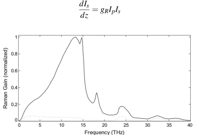
Fig. 2.1 Normalized Raman gain for fused silica when pump and stokes wave are copolarized (After [1])
where gR is the Raman gain coefficient, Is is the stokes intensity, whileIp is
the pump intensity.
The Raman gain spectrum for silica, gR(Ω), where Ω is the frequency
difference between the pump and stokes waves, shown in Fig. 2.1, is found to be very broad, extending up to 40 THz with a peak located near 13 THz [48]. As long as the frequency difference Ωlies within the bandwidth of the
Raman gain spectrum, the beam launched at the fibre input will be amplified because of the Raman gain. The maximum gain in silica is achieved for the frequency component downshifted by about 13 THz from the pump frequency. SRS exhibits a threshold like behaviour, implying that significant conversion of pump energy to stokes energy occurs when the pump intensity exceeds a threshold level. For a single mode fibre, assuming Lorentzian shape approximation for the Raman gain spectrum, the SRS threshold pump intensity is given by
IPth≈16 Aeff
gRLeff
2.3.7 Dispersive waves
The emission of fundamental solitons is accompanied by a low amplitude temporal pedestal that propagates in a linear regime [50]. Fundamental solitons are susceptible to perturbations such as higher order dispersion and the resultant instability manifests as a nonsolitonic radiation (NSR) at a particular frequency [51]. Essentially, a resonance condition involving higher order dispersion terms comes into play and leads to a coherent enhancement of the NSR at a narrow band of frequencies as predicted by the appropriate phasematching condition. This enhanced spectral component (which occurs in the normal dispersion regime of the waveguide) is sometimes also referred to as a Cherenkov radiation or soliton induced resonant emission. Cherenkov radiation is a terminology borrowed from particle physics and it appears when a particle travels faster than the phase velocity of light in the medium [52]. The analog of this effect in optical waveguides is the resonance that occurs between the pulse, which travels at its group velocity, and the dispersive wave resulting in an energy transfer from the soliton to the dispersive wave at a frequency dictated by the appropriate phasematching condition.
The frequency of the dispersive wave that grows because of radiation emitted by the perturbed soliton can be obtained by a simple phasematching argument requiring that the dispersive wave propagate with the same phase velocity as that of the soliton. If ω andωs are frequencies of the dispersive
wave and of the soliton, respectively, the two phases at a distance z after a delayt =z/vg are given by [1]
φ(ω) =β(ω)z−ω(z/vg) (2.51)
φ(ωs) =β(ωs)z−ωs(z/vg) +
1
where vg is the group velocity of the soliton. The last term in Equation (2.52)
is due to the nonlinear phase shift occurring only for solitons. The two phases are equal when the following phasematching condition is satisfied
β(ω) =β(ωs) +β1(ω−ωs) +
1
2γPs (2.53) where the relation vg=1/β1 is used for the solutions of this equation which
determine the frequencyω of one or more dispersive waves generated because
of soliton perturbation.
The generation of dispersive waves during soliton fission is sensitive to minute details of the dispersion relation β(ω) of the waveguide, and it may
be necessary in some situations to include dispersion terms even higher than the fourth order. A numerical approach with multiple higher-order dispersion terms shows that all odd-order terms generate a single NSR peak on the blue or the red side of the carrier frequency of the pulse, depending on the sign of the corresponding dispersion parameter [1]. In contrast, even-order dispersion terms with positive signs always create two NSR peaks on opposite sides of the carrier frequency [1]. It will be shown in details how two NSR produced in a two ZDW waveguide later in Chapter 5.
2.4
Summary
Numerical Methods
This chapter presents the numerical methods for analyzing the properties of optical waveguides based on the Maxwell’s equations and the generalized nonlinear Schrödinger equation (GNLSE) introduced in Chapter 2. Section 3.1 reviews the light guidance mechanisms of optical waveguides briefly. The finite-element (FE) method is used for yielding the linear properties of the optical waveguides in Section 3.2. Finally, Section 3.3 describes split-step Fourier method (SSFM) to solve GNLSE for observing propagation dynamics of optical signal through SC generation in waveguide output.
3.1
Optical waveguides
ge-Core, n1
Substrate, ns
Cladding, n0
(a)
Core
ᴧ d Air-hole
(b)
Fig. 3.1 Schematics of (a) planar (channel) waveguide and (b) PCF with hexagonal symmetry cladding containing air-holes.
ometries (rib/channel) are being considered as index guiding waveguides for SC sources owing to scalable, low cost fabrication and the potential for inte-grated optical chip solutions [21]. An example of PBG guiding waveguides is the hollow core fibres [58].
Standard step-index fibres consist of a cylindrical glass core surrounded by a cladding, with the cladding having a slightly lower index than the core [1]. Planar channel/rib waveguides consist of a square or rectangular core surrounded by a cladding with lower refractive index than that of the core shown in Fig. 3.1(a). Light can be confined in the core due to total internal reflection at the interface between core and cladding in index guiding waveguides [53]. PCF relies on an effective index difference between the solid core and the surrounding cladding containing air-holes for a modified total internal reflection guiding mechanism [54] shown in Fig. 3.1(b). PBG guiding waveguide offers a fundamentally different way of guiding the light in it. The photonic band gap effect makes it possible to guide the light in a hollow air-core, surrounded by a cladding containing air-holes [59, 60].
To be able to calculate these propagation characteristics, solutions of the well-known Maxwell’s equations are obtained along with the satisfaction of the necessary boundary conditions. Applying the Maxwell’s equations may not be an easy task and precise analyses of optical waveguides is gen-erally considered to be a difficult task because of some major reasons such as the optical waveguides may have complex structures, arbitrary refractive index distribution (graded-index optical waveguides or photonic crystal fi-bres), anisotropic and nonlinear optical materials as well as materials with complex refractive index such as semiconductors and metals. These diffi-culties are surmounted using various methods of optical waveguide analyses developed. These methods can be broadly classified into two groups, namely the analytical approximation solutions and the numerical solutions. An exact analytical solution can be obtained for step-index two-dimensional optical waveguides (planar waveguides) and step-index fibre (SIF). However, if the waveguide has an arbitrary refractive index distribution such as PCFs and graded-index fibres, then the exact solutions may not be possible. Since we also consider here PCFs that do not have analytical solution, a finite-element based numerical method (FE mode-solver) is used for analyzing all optical waveguides proposed.
(rib/channel) waveguides and microstructured fibres (MoFs) for designing broadband mid-infrared SC laser sources.
3.2
Finite-element method
The rapid growth in the millimetre-wave, optical fibre and integrated optics fields has included the use of arbitrarily shaped dielectric waveguides, which in many cases also happened to be arbitrary inhomogeneous and/or arbitrar-ily anisotropic which do not easarbitrar-ily lend themselves to analytical solutions. Therefore many scientists have given their attention to the development of numerical methods to solve such waveguides. Numerical methods may be used to solve Maxwell’s equations exactly and the results they provide are accurate enough for the characterisation of most of the devices. Since the ad-vent of computers with large memories, considerable attention has been paid to methods of obtaining numerical solutions of the boundary and initial value problems. These methods are usually evaluated in terms of their generality, accuracy, efficiency and complexity. It is evident from the review articles [61] that every method represents some sort of compromise between these aspects, implying that no method is superior to the others in all aspects. The optimal method should be the one that can solve the problem with acceptable accuracy but requires the minimum effort to implement and run in terms of manpower and computer capacity. The FE method has been the dominant and arguably the most powerful numerical method in computational mechanics for many decades. It has been successfully applied to solve problems encountered in many engineering disciplines such as fluid dynamics, heat conduction, aeronautical, biomechanical and electromagnetics.
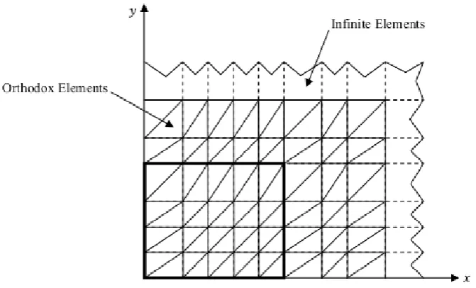
waveg-uides with any refractive index distribution and to those with any anisotropic materials or nonlinear materials. This method is based upon dividing the problem region into a non-overlapping patchwork of polygons, usually tri-angular elements. The field over each element is then expressed in terms of polynomials weighted by the fields over each element. By applying the variational principle to the system functional, and thereby differentiating the functional with respect to each nodal value, the problem reduces to a standard eigenvalue matrix equation. This is solved using iterative techniques to obtain the propagation constants and the field profiles [64, 68]. The accuracy of the finite element method can be increased by using finer mesh. A number of for-mulations have been proposed, however, the full vectorialH-field formulation is the most commonly used and versatile method in modelling optical waveg-uides due to much easier treatment of the boundary conditions. This method can accurately solve the open type waveguide problems near cut-off region and much better results were obtained by introducing infinite elements to ex-tend the region of explicit field representation to infinity [63]. One drawback associated with this powerful vector formulation is the appearance of spurious or non-physical solutions. Suppression of these spurious solutions can be achieved by introducing a penalty term into the variational expression [65]. In order to eliminate the spurious solutions completely, another approach is employed using the edge elements [62, 68]. In modelling more complex structures, the finite element method is considered to be more flexible than the finite difference method due to the ability of employing irregular mesh. Since this method is used in this work, a more detailed description of the finite element method will be presented next.
defined by a governing differential equation in a domain, together with the boundary conditions on the boundary that encloses the domain. In the varia-tional approach the boundary-problem is formulated in terms of variavaria-tional expressions, referred to as functionals, whose minimum corresponds to the governing differential equations. The approximate solution is obtained by minimising the functional with respect to its variables [66]. The Galerkin method is based on the method of weighted residuals [67] in which the domain of the differential equation is discretized and the solution is approximated by the summation of the unknown solutions of each subdomain weighted by known functionals, relating them to the domain. The overall solution is obtained by minimising the error residual of the differential equation. Varia-tional Formulation, while much less intuitive, is more advantageous as the underlying theory is more involved. Therefore, Variational Formulation is an ideal technique to solve a wide range of electromagnetic problems, which is used in FE method in this thesis.
3.2.1 The variational approach
There are several variational formulations for implementing FE method have been proposed for the analysis of the optical waveguide problem. These can be a scalar form [69], where the electric or magnetic field is expressed only in terms of one component, according to the predominant field component or can be in the vector form, where the electric or magnetic field is expressed in terms of at least two of the constituent field components.
It should be noted that most of the formulations applied in the FE method, yield to a standard eigenvalue equation
[A]{x} −λ[B]{x}=0 (3.1)