An integrated nonlinear optical loop mirror in silicon
photonics for all-optical signal processing
Zifei Wang,1Ivan Glesk,2and Lawrence R. Chen1
1Department of Electrical and Computer Engineering, McGill University,
3480 University Street, Montr´eal, Quebec H3A 0E9, Canada
2Department of Electronic and Electrical Engineering, University of Strathclyde,
Glasgow, Scotland G1 1XU, United Kingdom
(Received 13 November 2017; accepted 21 January 2018; published online 5 February 2018)
The nonlinear optical loop mirror (NOLM) has been studied for several decades and has attracted considerable attention for applications in high data rate optical com-munications and all-optical signal processing. The majority of NOLM research has focused on silica fiber-based implementations. While various fiber designs have been considered to increase the nonlinearity and manage dispersion, several meters to hundreds of meters of fiber are still required. On the other hand, there is increas-ing interest in developincreas-ing photonic integrated circuits for realizincreas-ing signal processincreas-ing functions. In this paper, we realize the first-ever passive integrated NOLM in sili-con photonics and demonstrate its application for all-optical signal processing. In particular, we show wavelength conversion of 10 Gb/s return-to-zero on-off keying (RZ-OOK) signals over a wavelength range of 30 nm with error-free operation and a power penalty of less than 2.5 dB, we achieve error-free nonreturn to zero (NRZ)-to-RZ modulation format conversion at 10 Gb/s also with a power penalty of less than 2.8 dB, and we obtain error-free all-optical time-division demultiplexing of a 40 Gb/s RZ-OOK data signal into its 10 Gb/s tributary channels with a maximum power penalty of 3.5 dB. ©2018 Author(s). All article content, except where oth-erwise noted, is licensed under a Creative Commons Attribution (CC BY) license (http://creativecommons.org/licenses/by/4.0/).https://doi.org/10.1063/1.5013618
Continued increases in traffic demand impose considerable strain on current optical trans-mission/transport systems and networks. Coherent systems have been adopted to cope with this strain by enabling the use of higher-order and spectrally efficient modulation formats, thereby increasing channel capacity.1,2 While there is significant focus on coherent systems, all-optical signal processing, which avoids optical-to-electrical-to-optical conversion and can support ultra-high operating speeds, is still being considered as a means to perform certain functions such as switching or routing and may be especially useful in situations where individual bits do not need to be “touched.”3,4 Additional signal processing functions include wavelength conversion and multi-casting,5,6optical time-division multiplexing/demultiplexing (OTDM),7–10signal regeneration,11,12 optical modulation,13 and Fourier transformation.14All-optical signal processing is also useful for applications beyond the optical transmission/transport, such as instrumentation, including all-optical sampling for waveform measurement,15 analog-to-digital or digital-to-analog conversion,16,17 and photonic radio-frequency spectrum analysis;18mode locking of lasers;19 and generating arbitrary waveforms.4
All-optical signal processing typically exploits ultrafast nonlinear optical effects such as self-phase modulation, cross self-phase modulation (XPM), and four-wave mixing (FWM). XPM has the advantage of being more robust to phase-matching and high power efficiency, which is suitable for applications involving amplitude modulated signals. One approach to implement signal processing operations is to exploit XPM in a nonlinear medium followed by bandpass filtering to extract either the red- or blue-shifted sideband of the broadened spectrum.20,21However, the filtering process can reduce significantly the power received by a detector thereby impacting negatively signal processing performance. An alternate technique involves converting the XPM-induced phase modulation into
amplitude modulation using an interferometric structure. To this end, Mach-Zehnder interferometers (MZIs)22,23 and nonlinear optical loop mirrors (NOLMs)24 have been investigated. Compared to MZIs, NOLMs are simple and have inherently a balanced interferometer configuration. The NOLM has been studied for several decades, and many applications in optical communications and all-optical signal processing have been realized, e.g., 2-bit all-optical digital-to-analog conversion, optical perfor-mance monitoring, wavelength conversion (including from the O-band to the C-band), ultrawideband pulse generation, and demultiplexing of optical time-division multiplexed (OTDM) signals as high as 1.28 Tb/s.6,8,25–32
Almost all reported NOLMs are based on silica fiber. Because of a generally weak nonlinear coefficient, the length of the fiber loop is on the order of several meters to hundreds of meters, which is evidently unsuitable for developing integrated all-optical signal processing subsystems. Zhuang
et al.recently reported an integrated NOLM incorporating a semiconductor optical amplifier (SOA) in indium phosphide for all-optical sampling.33 However, the sampling window is ∼30 ps due to the saturation time in the SOA and as such is not suitable for processing ultrahigh speed signals. Various nonlinear materials have been considered to exploit the femtosecond response of Kerr-based nonlinearities for use in passive integrated devices for all-optical signal processing, e.g., AlGaAs,34 chalcogenide,10,35silicon,36and silicon nitride.37,38Silicon-on-insulator (SOI) has a number of desir-able characteristics such as compatibility with CMOS technology, strong light confinement, and large Kerr nonlinear coefficient36 that make it desirable for creating a passive integrated NOLM. In this paper, we report the first-ever passive integrated NOLM in SOI and demonstrate its applica-tion for all-optical signal processing. In particular, we perform wavelength conversion of 10 Gb/s return-to-zero on-off keying (RZ-OOK) signals over a wavelength range from 1535 nm to 1565 nm, 10 Gb/s nonreturn to zero (NRZ)-to-RZ modulation format conversion, and OTDM demultiplexing a 40 Gb/s RZ-OOK data signal into its four 10 Gb/s tributary channels. Due to the short length and low dispersion of the nonlinear waveguide, the switching window of the NOLM can be extremely short and support even higher rates of operation.
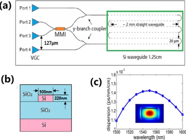
Figure1(a)illustrates a schematic of the integrated NOLM in SOI. It is a four-port device where vertical grating couplers (VGCs) are used for input and output coupling. The VGCs39are designed for C-band TE mode operation and have a 3 dB bandwidth of∼15 nm; the minimum coupling loss
[image:2.594.144.451.472.704.2](i.e., at the peak wavelength of the VGC spectral response) is typically 7.5 dB/coupler. The various silicon waveguides in the device have a height of 220 nm and sit on top of a 3µm thick oxide; they are covered by a 2µm thick index-matched oxide cladding. Ports 2 and 3 of the NOLM are connected to a 3 dB multimode interferometer (MMI) coupler. The MMI coupler is based on a multimode waveguide having a width of 6µm and a length of 128µm. The single mode input and output waveguides to the MMI are separated by 3µm (all single mode waveguides in the device have the same cross section). In the loop, we use a silicon waveguide having a total length of 12.5 mm; it employs a serpentine configuration with waveguide bends having a bend radius of 10 µm and straight segments having a length of 2 mm. Ports 1 and 4 of the NOLM are connected to the loop via 3 dB Y-branch power splitters; they serve to couple in the pump signals and for monitoring. The probe signals are launched into the NOLM via port 2, while the output is extracted from port 3. The four VGCs are placed in a row at the same end of the device with a pitch of 127 µm to match the fiber-to-fiber spacing of a fiber ribbon array. The NOLM is fabricated using e-beam lithography with a single etch, and the total size is∼2.65 mm×0.41 mm. Separate test structures reveal a waveguide propagation loss of ∼2.7 dB/cm. The loss for a (pump) signal from port 1 to port 3 is∼27 dB. In the absence of a pump signal (i.e., for linear operation of the loop mirror), the loss for a (probe) signal launched into port 2 and which also exits port 2 (and is subsequently extracted using an off-chip optical circulator) is ∼24 dB (this loss accounts for the 15 dB loss from the VGCs, the losses from the couplers used to combine the pump with the probe in the loop, and waveguide propagation loss). The device is not mounted nor packaged, and while no specific temperature control is used, we do not observe any short nor medium term effects due to temperature sensitivity/drift.
Previously, we investigated the impact of waveguide design parameters on FWM conversion efficiency and found that a waveguide cross section of 220 nm×500 nm (height×width) and a length of 12 mm were optimal in terms of balancing the nonlinear effects with dispersion and loss.40 As such, we use nominally the same parameters for the waveguide in the NOLM. The single mode silicon waveguides have a width of 500 nm [the cross section appears in Fig.1(b)] and are designed to support largely the fundamental TE mode, as shown in the inset of Fig.1(c). The effective area
Aeff of the fundamental mode is calculated to be 0.065 µm2. Using a nonlinear index in silicon
of n2 = 4.5×10¹⁸ m2 W1,41 we estimate the nonlinear coefficient γ to be 282.7 m1 W1 at 1550 nm. The simulated total dispersion of the silicon waveguide is shown in Fig. 1(c); at 1550 nm, it is 1.42×10³ ps/(nm cm). Due to the short length of the waveguide in the loop and the use of picosecond pump pulses, walk-off between the pump and probe is negligible and can be ignored so that the switching window of the NOLM should be similar to the duration of the pump pulses.42
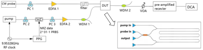
[image:3.594.123.473.620.707.2]First, we demonstrate wavelength conversion of 10 Gb/s RZ-OOK signals. In the integrated NOLM wavelength converter, a continuous wave (CW) signal (probe) is gated by the RZ-OOK signal (pump) via XPM.27Figure2illustrates the experimental setup. A 10 Gb/s RZ-OOK signal is obtained by modulating the output pulses from a 10 GHz mode-locked laser using an electro-optic Mach-Zehnder modulator (MZM) driven by a 231 1 pseudo-random bit sequence (PRBS) from a pulse pattern generator (PPG). The 10 Gb/s RZ-OOK signal is then amplified by a high power erbium-doped fiber amplifier (EDFA) and filtered by a wavelength-division-multiplexing (WDM) coupler to remove the amplified spontaneous emission (ASE) noise. After amplifying and filtering,
the pulses are∼15 ps; the duty cycle of the pump launched into the device (at port 1) is thus 15%. The CW probe is generated by a tunable laser; it is amplified, filtered using an optical bandpass filter with a 3 dB bandwidth of 0.3 nm, and coupled into the chip (via port 2). The output from the NOLM (at port 3) is filtered using another WDM coupler to remove the residual pump; the wavelength converted signals are detected using a pre-amplified receiver [for bit error rate (BER) measurements] and a digital communications analyzer (DCA). The average input power of the pump and CW probe prior to coupling into the VGCs is 21 dBm and 18 dBm, respectively. Note that once we account for the VGC loss (∼7.5 dB) and the 3 dB coupling loss due to the coupler that combines the pump with the probe signal, the average powers of the pump and CW probe in the waveguide (nonlinear loop) where XPM occurs are 10.5 dBm and 4.5 dBm, respectively. While two photon absorptions can occur in silicon waveguides, for the input powers used, we do not observe any nonlinear losses.42
We fix the central wavelength of the pump to 1550 nm and vary the probe wavelength from 1535 nm to 1565 nm. The results are summarized in Fig.3: (a) illustrates clearly XPM-based broad-ening around the probe as its wavelength is tuned over the 30 nm range. Based on the amount of spectral broadening about the probe carrier, the estimated nonlinear phase shift is∼0.4π. This is greater than the nonlinear phase shift calculated usingϕmax= 2γPPLeff (wherePPis the peak power
of the pump and Leff is the effective length of the nonlinear waveguide in the loop) which gives a value of ∼0.4. We believe that the discrepancy is due to the measured duty cycle of the pump pulses and, in particular, the limitation of our detection system which has an impulse response time >10 ps (we obtain good agreement between the measured and simulated spectral broadening when the pump pulses are ∼6 ps). Note that the maximum XPM conversion efficiency, defined here as the ratio between the input pump power launched into the chip at port 1 and the peak of the XPM-broadened spectra about the probe signal at the output of the chip at port 3, is46 dB for a probe wavelength of 1535 nm (which can be improved with VGCs having lower coupling loss). Figure3(b)
shows the measured BER of the wavelength converted signals at 1535 nm, 1540 nm, 1560 nm, and 1565 nm. We obtain error-free operation (BER<109) with a maximum power penalty of 2.5 dB for the wavelength converted signal at 1560 nm. The eye diagrams are clearly open, and the switching window shown on the DCA, which is extracted from the duration of the broadest eye diagram, is at most 16.5 ps. This is similar to the duration of the eye diagram for the back-to-back signal (15 ps shown on the DCA) and confirms that the switching window is given largely by the duration of the pump pulses. Note that the measured switching times (and duration of pulse widths) are limited by the response time of the detection system (receiver and DCA). We attribute variations in the charac-teristics of the wavelength converted signals to spectral variations in the VGC response (which can cause fluctuations in the coupled power).
Next, we demonstrate NRZ-to-RZ modulation format conversion at 10 Gb/s. The experimental setup is similar to that used for wavelength conversion except that a 10 Gb/s NRZ-OOK signal is used as the probe rather than a CW signal and the pump is given by the amplified mode-locked laser pulses. We use a tunable optical delay to optimize the position of the pump pulses to coincide with the maximum extinction ratio of the NRZ signal in the time domain. The principle is based on the XPM-induced phase shift on the NRZ probe signal at the instants in time when there is overlap with the pump pulses. The phase shift is proportional to the power of the pump pulses, and after interfering in the loop, the probe waveform will have the same shape as the pump pulses,41,43i.e., the pump pulses carve out a portion of the NRZ signal to create the converted RZ signal, see Fig.4(a). The 10 Gb/s NRZ-OOK signal is generated by modulating the output from a tunable laser at 1560 nm with a 2311 PRBS. The wavelength of the pump is set to 1550 nm. The average input powers of the NRZ signal and the pump before coupling into the VGCs are 18 dBm and 21 dBm, respectively. Figures4(b)and4(c)show the measured BER and eye diagrams at error-free operation for the original NRZ and the converted RZ signals. We obtain a clear open eye for the converted signal with a power penalty of 2.8 dB. Note that the power penalty is similar to that obtained for wavelength conversion involving the same wavelengths for the pump and CW probe signals (i.e., 1550 nm and 1560 nm, respectively).
FIG. 3. (a) Output spectra from the integrated NOLM. The pump is located at∼1550 nm, and the probe varies from 1535 nm to 1565 nm. (b) Measured BER of the back-to-back (B2B) and wavelength converted RZ-OOK signals and (c) corresponding eye diagrams (measured at a received power corresponding to a BER = 109).
[image:5.594.141.448.82.579.2]FIG. 4. (a) Principle of NRZ-to-RZ modulation format conversion, (b) measured BER vs. received power, and (c) eye diagrams at error-free operation of the original NRZ and converted RZ signals.
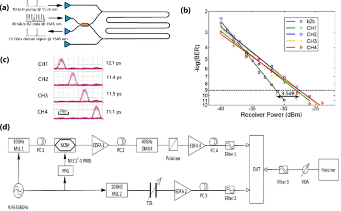
11 ps after amplifying and filtering, which is shorter than that in the 40 Gb/s signal. The average input power of the 40 Gb/s RZ-OOK signals and the 10 GHz pump is 15 dBm and 19 dBm, and the corresponding central wavelengths are 1545 nm and 1558 nm. The experimental setup is illustrated in Fig.5(d). As shown in Fig.5(b), we obtain error-free operation for all four demultiplexed tributary
[image:6.594.142.453.85.346.2] [image:6.594.125.472.479.694.2]channels with a maximum power penalty of 3.5 dB. Figure5(c)shows the eye diagrams for the four demultiplexed tributary channels at a received power of27 dBm; the duration of the eye diagrams ranges from 11.1 ps to 12.1 ps and is close to the pulse width of the 10 GHz pump.
In the experiments involving modulation format conversion and OTDM demultiplexing, we fixed the pump and signal wavelengths. Note that wavelength conversion over a broader range of 30 nm was obtained, and as such, we expect to be able to operate NRZ-to-RZ modulation format conversion and OTDM demultiplexing over a broader wavelength range.
We now discuss several important aspects of our integrated NOLM. First, as mentioned pre-viously, we obtained a maximum XPM conversion efficiency of46 dB and this is constrained in large part by the relatively large loss of the VGCs. Recently, VGCs with significantly lower loss have been demonstrated: for example, Dinget al.reported a coupling efficiency of∼87%44while Zhuet al.achieved∼93%.45It is also possible to use edge coupling, whereby the silicon waveg-uides can be tapered and combined with a polymer overlay waveguide; in this case, a coupling loss of 2.6 dB per facet was obtained.3The use of such VGC designs or edge coupling approaches will improve the XPM conversion efficiency and/or reduce the necessary launched power levels. Second, our integrated NOLM is based on SOI. However, it can be implemented in other non-linear materials/platforms such as silicon nitride (including silicon-rich nitride) and chalcogenide. As these materials involve smaller refractive index contrasts, the waveguide cross sections can be larger which can support more readily edge coupling. Moreover, while the nonlinear coefficient of silicon nitride (or chalcogenide) is less than that of silicon, there is no nonlinear absorption. Third, it may be possible to implement polarization diversity schemes for polarization independent operation as on-chip polarization beam splitters and combiners are available.46,47However, the structure may be more complex as the optimal dimensions of an SOI waveguide for maximum nonlinearity for TM modes and TE modes are very different.48One solution is to use a nonlinear material as a cladding of the SOI waveguide for TM modes.36 Furthermore, the measured switching times of the NOLM correspond largely to the duration of the pump pulses (due to the low dispersion in the waveguide). By using shorter pump pulses, the integrated NOLM should be able to support even higher rates of operation. Finally, we compare the performance of our integrated NOLM to a NOLM based on silica-based highly nonlinear fiber (HNLF). For typical silica-based HNLF, the nonlinear coefficient is ∼11.5 W1km1and the loss is∼0.9 dB/km.49For an HNLF length of 1 km and the same amount of pump power in the nonlinear waveguide as in our experiment (and assuming a duty cycle of 15%), the nonlinear phase shift would be∼4 times greater compared to that from our integrated NOLM. Thus, in order to have comparable performance to a NOLM based on HNLF, the nonlinearity or the effective length of the nonlinear waveguide needs to increase. One possibility is to use silicon-rich nitride as the material platform;38 while the nonlinear coefficient is less than silicon, the loss can be much lower allowing for a longer length of nonlinear waveguide. Using silicon for the nonlinear waveguide will constrain the NOLM switching performance in the sense that the maximum extinction ratio may not be attainable as the power required to obtain aπphase shift will likely induce nonlinear absorption.
We have presented the first passive NOLM in SOI and successfully demonstrated XPM-based wavelength conversion of 10 Gb/s RZ-OOK signals, 10 Gb/s NRZ-to-RZ modulation format con-version, and OTDM demultiplexing from 40 Gb/s to 10 Gb/s. We believe that the passive inte-grated NOLM will allow for the implementation of more advanced (and inteinte-grated) ultrahigh speed all-optical signal processing subsystems.
The devices were fabricated at the University of Washington Nanofabrication Facility, a member of the National Science Foundation National Nanotechnology Infrastructure Network. We thank the Natural Sciences and Engineering Research Council of Canada (NSERC) CREATE programs (NGON and Si-EPIC), the Royal Society, and the European Union Horizon 2020 research and innovation program under the Marie Skłodowska-Curie Grant Agreement No. 734331 for financial support. We also thank Dr. Junjia Wang and Rhys Adams for discussions.
1I. Roudas, “Coherent optical communication systems,” inWDM Systems and Networks(Springer, New York, 2012),
p. 373.
2T. A. Eriksson, T. Fehenberger, P. A. Andrekson, M. Karlsson, N. Hanik, and E. Agrell,J. Lightwave Technol.34, 2256
3L. K. Oxenløwe, H. Jia, M. Galili, M. Pu, H. Hu, H. C. H. Mulvad, K. Yvind, J. M. Hvam, A. T. Clausen, and P. Jeppesen, IEEE J. Sel. Top. Quantum Electron.18, 996 (2012).
4A. E. Willner, S. Khaleghi, M. R. Chitgarha, and O. F. Yilmaz,J. Lightwave Technol.32, 660 (2014). 5S. J. B. Yoo,J. Lightwave Technol.14, 955 (1996).
6G. Contestabile, A. Maruta, S. Sekiguchi, K. Morito, M. Sugawara, and K. Kitayama,IEEE J. Quantum Electron.47, 541
(2011).
7B.-E. Olsson and D. J. Blumenthal,IEEE Photonics Technol. Lett.13, 1005 (2001).
8A. Bogoni, P. Ghelfi, M. Scaffardi, and L. Poti,IEEE J. Sel. Top. Quantum Electron.10, 192 (2004).
9X. Wu, A. Bogoni, J. Wang, H. Huang, S. Nuccio, O. F. Yilmaz, and A. E. Willner, in Proceedings of Conference on Optical
Fiber Communication, Los Angeles, CA, 6–10 March 2011.
10B. J. Eggleton, B. Luther-Davies, and K. Richardson,Nat. Photonics5, 141 (2011).
11R. Salem, M. A. Foster, A. C. Turner, D. F. Geraghty, M. Lipson, and A. L. Gaeta,Opt. Express15, 7802 (2007). 12R. Salem, M. A. Foster, A. C. Turner, D. F. Geraghty, M. Lipson, and A. L. Gaeta,Nat. Photonics2, 35 (2008). 13H. Hu, M. Pu, H. Ji, M. Galili, H. C. H. Mulvad, K. Yvind, J. M. Hvam, P. Jeppesen, and L. K. Oxenløwe, in Proceedings
of Conference on Optical Fiber Communication, Los Angeles, CA, 4–8 March 2012.
14K. Goda and B. Jalali,Nat. Photonics7, 102 (2013).
15S. Fischer, M. Bitter, M. Caraccia, M. Dulk, E. Gamper, W. Vogt, and W. Hunzider,Opt. Lett.26, 626 (2001). 16S. Oda and A. Maruta,IEEE Photonics Technol. Lett.17, 465 (2005).
17S. Oda and A. Maruta,IEEE Photonics Technol. Lett.18, 703 (2006). 18C. Dorrer and D. N. Maywar,J. Lightwave Technol.22, 266 (2004).
19G. I. Stegeman, D. J. Hagan, and L. Torner,Opt. Quantum Electron.28, 1691 (1996). 20B. Olsson and D. J. Blumenthal,IEEE Photonics Technol. Lett.13, 875 (2001).
21W. Astar, J. B. Driscoll, X. Liu, J. I. Dadap, W. M. J. Green, Y. A. Vlasov, G. M. Carter, and R. M. Osgood,J. Lightwave Technol.28, 2499 (2010).
22S. Nakamura, Y. Ueno, and K. Tajima,IEEE Photonics Technol. Lett.13, 1091 (2001).
23I. Glesk, P. J. Bock, P. Cheben, J. H. Schmid, J. Lapointe, and S. Janz,Opt. Express19, 14031 (2011). 24N. J. Doran and D. Wood,Opt. Lett.13, 56 (1988).
25M. Jinno and T. Matsumoto,IEEE Photonics Technol. Lett.2, 349 (1990). 26T. Yamamoto, E. Yoshida, and M. Nakazawa,Electron. Lett.34, 1013 (1998).
27T. Sakamoto, F. Futami, K. Kikuchi, S. Takeda, Y. Sugaya, and S. Watanabe,IEEE Photonics Technol. Lett.13, 502 (2001). 28H. Sotobayashi, C. Sawaguchi, Y. Koyamada, and W. Chujo,Opt. Lett.27, 1555 (2002).
29M. Nakazawa, inProceedings of Nonlinear Optics: Materials, Fundamentals and Applications(Optical Society of America,
Wailea, HI, 29 July–2 August 2002).
30R. Adams, M. Rochette, T. T. Ng, and B. J. Eggleton,IEEE Photonics Technol. Lett.18, 469 (2006). 31T. Huang, J. Li, J. Sun, and L. R. Chen,IEEE Photonics Technol. Lett.23, 1255 (2011).
32T. Huang, S. Fu, J. Li, L. R. Chen, M. Tang, P. Shum, and D. Liu,Opt. Express21, 6401 (2013).
33L. Zhuang, C. Zhu, B. Corcoran, Z. Geng, B. Song, and A. Lowery, in Proceedings of European Conference on Optical
Communication, Dusseldorf, Germany, 16–20 September 2016.
34M. J. LaGasse, K. K. Anderson, C. A. Wang, H. A. Haus, and J. G. Fujimoto,Appl. Phys. Lett.56, 417 (1990).
35V. G. Ta’eed, M. Shokooh-Saremi, L. Fu, D. J. Moss, M. Rochette, I. C. M. Littler, B. J. Eggleton, Y. Ruan, and B.
Luther-Davies,Opt. Lett.30, 2900 (2005).
36J. Leuthold, C. Koos, and W. Freude,Nat. Photonics4, 535 (2010).
37D. T. H. Tan, K. Ikeda, P. C. Sun, and Y. Fainman,Appl. Phys. Lett.96, 061101 (2010).
38M. Rezagholipour Dizaji, C. J. Kr¨ukel, A. F¨ul¨op, P. A. Andrekson, V. Torres-Company, and L. R. Chen,Opt. Express25,
12100 (2017).
39A. Mekis, S. Gloeckner, G. Masini, A. Narasimha, T. Pinguet, S. Sahni, and P. De Dobbelaere,IEEE J. Sel. Top. Quantum Electron.17, 597 (2011).
40L. R. Chen, J. Li, M. Spasojevic, and R. Adams,Opt. Express21, 19624 (2013). 41M. Dinu, F. Quochi, and H. Garcia,Appl. Phys. Lett.82, 2954 (2003). 42G. P. Agrawal,Applications of Nonlinear Fiber Optics(Academic Press, 2014).
43G. Huang, Y. Miyoshi, A. Maruta, Y. Yoshida, and K.-I. Kitayama,J. Lightwave Technol.30, 1342 (2012). 44Y. Ding, C. Peucheret, H. Ou, and K. Yvind,Opt. Lett.39, 5348 (2014).
45L. Zhu, W. Yang, and C. Chang-Hasnain,Opt. Express25, 18462 (2017).
46E. A. El-Fiky, A. Samani, D. Patel, and D. V. Plant, in Proceedings of Conference on Optical Fiber Communication,
Anaheim, CA, 20–24 March 2016.
47J. R. Ong, T. Y. L. Ang, E. Sahin, B. Pawlina, G. F. R. Chen, D. T. H. Tan, S. T. Lim, and C. E. Png,Opt. Lett.42, 4450
(2017).
48C. Koos, L. Jacome, C. Poulton, J. Leuthold, and W. Freude,Opt. Express15, 5976 (2007).