International Journal of Innovative Technology and Exploring Engineering (IJITEE) ISSN: 2278-3075, Volume-8 Issue-8 June, 2019
Performance Analysis of Low Power 8-Tap FIR
Filter using PFAL
Premananda B.S., Ganavi M.G
Abstract : Power is the crucial criterion in the systems such as processors, filters and VLSI systems. The increase in the use of portable devices has increased the demand for low power devices. Finite Impulse Response (FIR) filter is one of the basic building blocks of Digital Signal Processor (DSP). FIR filter is the building block of DSP and can be realized by integrating adders, multipliers and delay elements. Adiabatic logic is one of the promising techniques to minimize power dissipation of static CMOS circuits. In this paper, 8-tap direct form-I FIR filter is realized by integrating Square Root Carry Select Adder (SQRT CSLA) using Binary to Excess-1 Converter (BEC), Reduced Complexity Wallace Tree Multiplier (RCWTM) and Barrel shifter. SQRT CSLA overcomes the problem of carry rippling delay in Ripple Carry Adder (RCA). SQRT CSLA using BEC overcomes the problem of power dissipation and area in SQRT CSLA using RCA by replacing equal sized blocks RCA with unequal sized RCA blocks. RCWTM reduces the area and power dissipation in Wallace tree multiplier by replacing compressors with adders. Both static CMOS and Positive Feedback Adiabatic Logic (PFAL) based direct form-I FIR filter are realized in Cadence Virtuoso (180 nm technology) and simulated in Spectre. PFAL based SQRT CSLA using BEC, RCWTM, Barrel shifter and realized 8-tap FIR filter dissipates 75.89 %, 81.03 %, 97.6 %, and 83.4 % less power when compared to static CMOS based circuits.
Keywords: Barrel shifter, CMOS, FIR, PFAL, Square Root Carry Select Adder, Wallace Tree Multiplier.
I. INTRODUCTION
Power is a critical parameter in the design of circuits. Increase in number of computations in the digital system increases the power dissipation, which necessitates the design of circuits using different low power techniques. Finite Impulse Response (FIR) filters have importance in the fields of DSP, image and video processing, and various other fields. The FIR filters are preferred due to its easy implementation and high stability. The key blocks required in the realization of the FIR filter are adders, multipliers and shifters which contribute to the area, delay and power dissipation of the circuit and hence, different methods have to be adopted to reduce the power dissipation [1]. FIR filters are digital filters whose response to a unit impulse (unit sample function) is finite in duration [2].
Carry generated by the adders such as RCA which causes delay in the circuit. This problem is overcome by implementing the modified adder architectures such as Carry Look-ahead Adder, Carry Save Adder (CSA), Carry Increment Adder and CSLA [3]. Parallel prefix adders have less delay but consume relatively large area. Different adder architectures are preferred for various applications.
Revised Manuscript Received on June 8, 2019.
Premananda B.S., Department of Telecommunication Engineering, RV College of Engineering,Bengaluru, India
Ganavi M.G., Department of Telecommunication Engineering, RV College of Engineering,Bengaluru, India
The carry rippling delay in the RCA can be minimized by implementing SQRT CSLA. The SQRT CSLA using RCA is not efficient w.r.t. area because of large number of RCAs [4]. This limitation is overcome by using BECs in the second stage of SQRT CSLA in place of RCAs which reduces the area thereby reducing the power dissipation of the circuit.
Multiplication is also an imperative arithmetic operation which is implemented using addition of partial products. Various multiplier architectures such as Array, Booth, Wallace, Dadda, Sequential and Vedic multipliers [11] exist. The power dissipation in the multiplier increases as more number of adders is used for partial product addition. This limitation is overcome by using Wallace tree multiplier (WTM), as it uses fewer adders and also reduces the number of computations as compared to conventional multiplier by grouping three rows of partial products into one group. The WTM is implemented using CSAs in which addition of three bits is possible at once, by storing carry in the present stage and adding it in the next stage [6]. The RCWTM reduces the area occupied by the WTM. The shifters may be realized based on combinational or sequential logic. The combinational (Barrel) shifters are efficient w.r.t. area and power. Barrel shifters are logic circuits that are used to rotate or shift data in a DSP which is an important part of a combinational logic block [7].
The power dissipation in the circuits can be minimized by employing various low power techniques. Adiabatic Logic (AL) demonstrates to be an efficient technique in minimizing the power dissipation. Adiabatic refers to a thermodynamic process in which the heat is not dissipated to the environment. The energy in the adiabatic systems is supplied back to the power clock [9]. There are two types of AL namely, full and quasi/partial adiabatic circuits.
The complete charge in the capacitance is recovered and provided to the power clock in case of full adiabatic circuits and in quasi adiabatic circuits only a part of energy is recovered back to the circuit [10]. Full adiabatic family can be Pass Transistor Adiabatic Logic (PAL), Split Rail Charge Recovery Logic (SCRL) and so on [22]. The partial/quasi adiabatic family includes Positive Feedback Adiabatic Logic (PFAL), Efficient Charge Recovery Logic (ECRL), NMOS Energy Recovery Logic (NERL), 2N-2N2P, True Single Phase Adiabatic Logic (TSEL), Clocked Adiabatic Logic (CAL), and Source Coupled Adiabatic Logic (SCAL). The circuit complexity is more in case of full adiabatic circuits than the quasi adiabatic circuits though the power dissipation is reduced in the former case. PFAL is an efficient adiabatic technique in which the power dissipation is less compared to other quasi adiabatic techniques.
insight into the literature is provided in section II. Section III provides the study of FIR filter and its sub-components. Section IV provides the design and implementation of direct form FIR filter, SQRT CSLA using RCA, SQRT CSLA using BEC, WTM, RCWTM and Barrel shifter using static CMOS logic and focuses on the description of PFAL, the working of AL circuits and the design of adiabatic circuits. Section V includes the design of the circuits in Cadence Virtuoso, simulation results obtained from the Spectre simulator and comparative analysis of CMOS and PFAL based adder, multiplier, shifter and direct form 8-tap FIR filter w.r.t. power dissipation at different frequencies. Section VI provides the conclusions and the future scope of the work.
II. LITERATURE REVIEW
Sheetal et al., [1] have proposed a power efficient 4-tap FIR filter using a combination of Modified Error Tolerant Adder (META) and Modified WTM (MWTM) in CMOS technology. The design has been implemented in Cadence Virtuoso. The results are compared with combinations of array multiplier and RCA, array multiplier and META, MWTM and RCA for estimation of power consumption, propagation and transistor count. The estimations inferred that the 4-tap FIR filter gives best performance.
The performance of the FIR filter implemented using WTM and truncated multiplier are compared by considering CSA in both the designs. The FIR filter is realized using Verilog HDL and simulated in Xilinx [2]. The author aimed to increase the speed and decrease the power of the multiplier in the FIR filter. The delay and power are less in case of truncated multiplier. The FIR filter implemented using WTM using CSA gives best results w.r.t. delay and power as compared to truncated multiplier.
A decision based CSLA is proposed in [3] where BEC is activated only when required. A comparison is made between decisions based CSLA and modified CSLA using BEC w.r.t. speed, area and power dissipation by synthesizing the design using Cadence RTL compiler. The power and area of the decision based CSLA is optimized by 17% and 11.57% compared to CSLA using BEC. The decision based CSLA is highly efficient w.r.t. area, speed and delay compared to regular CSLA and CSLA using BEC.
Abhiram et al., [4] have proposed a 32-bit, 64-bit and 128-bit SQRT CSLA based on the gate level modification for the regular CSLA. The circuits are realized using Verilog HDL and the performance parameters such as area, power and delay were analyzed using Synopsis tool using 90 nm technologies. The modified CSLA is analyzed and compared with conventional CSLA. The area and power are minimized in the modified CSLA with an increase in delay.
Different types of adders and multipliers are compared w.r.t. speed, power dissipation, number of transistors and power delay product values. CMOS 180 nm technology is used to design the circuits [13]. Array multipliers are easy to implement. Due to the irregular design in the WTM and Dadda multiplier, more number of transistors is used in the implementation. The power dissipation in the circuits depends on factors such as number of transistors, area, wiring, capacitances, etc.
Conventional CSLA and CSLA using BEC were designed and analyzed in both CMOS logic and ECRL using Cadence Virtuoso 180 nm technology [5]. The power dissipation of the CSLA using BEC is less compared to conventional CSLA. The delay in the CSLA using BEC is also reduced. The power dissipation and delay of 8-bit CSLA designed using ECRL is 84.6% and 93.1% less when compared to the adder designed using CMOS logic. ECRL is used to design the adders which prove to be an efficient technique in minimizing the power dissipation.
Vinay et al., [8] have proposed a signed and unsigned Baugh-Wooley and Braun multipliers, and the power and speed of the multipliers is analyzed. Multipliers are realized using CMOS, Split Path Data Driven Dynamic Logic (SPD3L) and Domino logic. Multipliers realized using Domino logic provides better results w.r.t. speed where the delay is minimized by 39% and 27% for Baugh Wooley and Braun multipliers. The delay in Braun multiplier using SPD3L is minimized by 26%. The SPD3L logic does not provide any improvement in minimizing the power dissipation, it rather increases the power dissipation in the circuits compared to CMOS design.
Barrel shifter operations which include right & left shifts; arithmetic and rotate operations are discussed with different types of Barrel shifters such as MUX-based, mask based and data reversal Barrel shifters [7]. Barrel shifters are evaluated based on the performance parameters such as area and delay. Mask based data reversal Barrel shifters are preferred when overflow and zero detection is required. Less area is consumed by data reversal Barrel shifters and less delay is produced by mask based Barrel shifters.
Nowrin et al., [16] have proposed a bidirectional n-bit reversible Barrel shifter, where n is an integer power of two. The shifter uses select inputs to shift (n-1) bits using log2n
bits. The reversible Barrel shifter is partitioned into three parts and a generalized approach is presented for each part to realize the whole architecture. The Barrel shifter is analyzed w.r.t. performance parameters such as quantum cost, number of gates and garbage outputs and it proves to be efficient w.r.t. all the parameters.
Alam et al., [9] have designed a 4-bit comparator using PFAL and ECRL in Cadence Virtuoso gpdk 180 nm technologies and compared it with the static CMOS logic w.r.t. power and area. ECRL and PFAL comparator provides 13.64 % and 54.54 % efficiency w.r.t. power compared to static CMOS design. The number of transistors is least in case of ECRL as compared to PFAL, which indicates that the area occupied by ECRL is less than PFAL.
AL is one of the promising approaches to minimize power dissipation of the devices. PFAL proves to be an efficient AL w.r.t. power. SQRT CSLA using RCA overcomes the delay caused by RCA. SQRT CSLA using BEC is efficient w.r.t. area and power as compared to SQRT CSLA using RCA. WTM is efficient w.r.t. area and power dissipation as compared to conventional multiplier such as Array multiplier. RCWTM is efficient w.r.t. area as compared to WTM. Barrel shifter is also efficient w.r.t. area due to its combinational
International Journal of Innovative Technology and Exploring Engineering (IJITEE) ISSN: 2278-3075, Volume-8 Issue-8 June, 2019
shifter are integrated to form direct-form-I FIR filter using both static CMOS logic and PFAL. The circuits designed using PFAL dissipates less power as compared to the circuits designed using static CMOS logic.
III. FIRFILTERANDITSSUB-COMPONENTS
A. Direct Form FIR Filter
FIR filter is the basic element of DSP system. The different structures of FIR filter are direct, canonical, pipelined and inverted form [17]. The key components of a FIR filter are adder, multiplier and shifter. The input samples are multiplied with filter coefficients and the products are accumulated by using an adder to produce appropriate result. The total power dissipation of the FIR filter depends on the power dissipation of the adders, multipliers and shifters. So, the efficient design of the adders, multipliers and shifters is necessary. For an N-tap FIR filter there are N multipliers and N-1 adders and delay elements or shifters. The delay elements shift the input by specified bit position. The multipliers convolute the co-efficient and the output of the delay element. The convolved outputs are added by using an efficient adder. In a 4-tap FIR filter there are three delay elements or shifters, three adders and four multipliers as shown in Figure 1.
The system function of a finite duration impulse response filter is,
10 1
1 1
1
0
....
)
(
M
n n n M
M
z
b
z
b
z
b
b
z
H
(1)The impulse response is,
else M n b
n
[image:3.595.291.551.411.569.2]h n
... 0
1 0
... )
(
(2)
The difference equation of FIR filter is provided by,
y
(
n
)
b
0x
(
n
)
b
1x
(
n
1
)
...
b
M1x
(
n
M
1
)
(3)Figure 1: Direct Form FIR Filter [18]
where,
x(n), x(n-1)…x(n-M+1) are input signals y(n) is output signal
b0, b1…bM-1- Impulse response or filter co-efficient M is Filter length, and
M-1 is order of the Filter
SQRT CSLA using BEC, RCWTM and Barrel shifter are used in the implementation of FIR filter. The FIR filters have linear phase, which means an input signal is delayed but the phase is not distorted [18].
B. Square Root Carry Select Adder using RCA
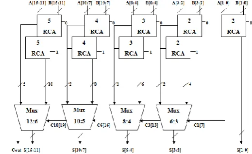
The design of any CMOS circuit requires the sizing of transistors first. In CMOS logic both pMOS and nMOS transistors are used. pMOS transistors are slower than nMOS since, mobility of electrons is greater than holes. They have different rise and fall times. Hence, to have symmetrical rise and fall times, sizing of the transistors is very important. SQRT CSLA using RCAs is constructed by integrating RCAs and multiplexers. The first two stages of SQRT CSLA are RCAs and the last stage which acts as a decision stage is realized using multiplexers. To overcome the problem of delay in the RCA, SQRT CSLA is used as shown in Figure 2. N-bit Binary inputs are divided into N groups to carry out the addition process, from which the name square root arises in SQRT CSLA. Each RCA group executes simultaneously depending on the inputs, thereby reducing the delay time than the RCA [3].
In 16-bit SQRT CSLA architecture, the first stage of RCAs compute the sum of two 16-bit numbers with CIN=„0‟ at each RCA block. The input of the first stage is propagated to the second stage which consists of RCAs where the two 16-bit input numbers are added with CIN=„1‟ [4]. Both the outputs of first and second stage RCAs are fed as input to the multiplexer (MUX). Another input to the multiplexer is a select line. The select line to a multiplexer is the COUT of the preceding multiplexer. If the select line, S = „0‟, the MUX selects the output of first stage and for S = „1‟, the MUX selects the output of second stage, thereby displaying the appropriate output.
Figure 2: 16-bitSQRT CSLA using RCA
C. Square Root Carry Select Adder using BEC
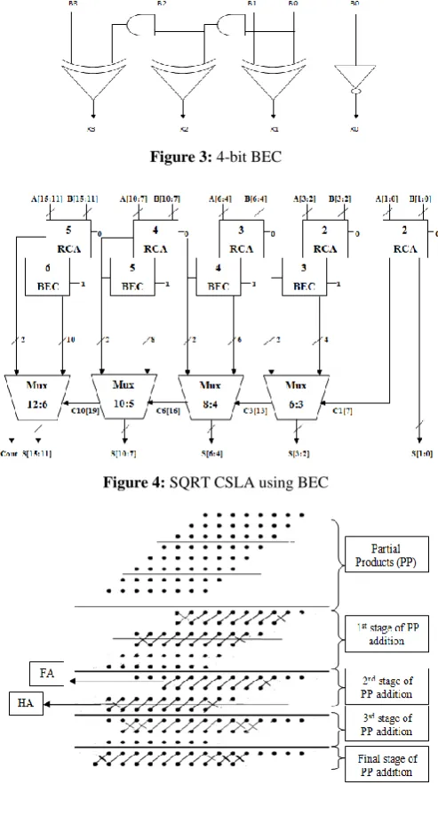
The use of multiple RCAs occupies more area, which is overcome by using BECs in place of RCAs in the second stage. This modification in conventional SQRT CSLA using RCA minimizes area and power dissipation. Architecture of SQRT CSLA using BEC is same as that of SQRT CSLA using RCA, except for the use of BEC in the second stage instead of RCA. A 4-bit BEC is depicted in the Figure 3. The SQRT CSLA using BEC is illustrated in Figure 4.
input to the second stage is the output of first stage. An n-bit RCA is replaced by n+1 n-bit BEC. The number of transistors in 4-bit BEC is 56.98% less as compared to the 3-bit RCA. The reduction in the number of transistors contributes to the decrease in the area occupied and the power dissipation. The BECs in the second stage automatically adds one to its input without the need for considering CIN=„1‟. The remaining operations follow the same procedure as in the SQRT CSLA using RCA. The outputs of both the first and second stage are fed to the multiplexers to select the appropriate output. SQRT CSLA using BEC is a high speed, low power and less area occupying adder which can be implemented in different applications [12].
D. Wallace Tree Multiplier
[image:4.595.46.293.348.812.2]Wallace tree multipliers are efficient w.r.t. area and speed. WTM is also power efficient and has high switching speed than Array multiplier. Multiplication process involves, generation of partial products, grouping of partial products and reduction, and finally partial product addition [2]. The partial products are formed by multiplying the inputs, three rows of partial products are considered as a single group as illustrated in Figure 5.
Figure 3: 4-bit BEC
Figure 4: SQRT CSLA using BEC
Figure 5: 8 x 8-Bit WTM [14]
Full Adders (FA) is used where there are three inputs and Half Adder (HA) is used where there are two inputs. The FA adds the inputs by following the procedure of carry save addition. FA retains the partial sum in the present stage and passes the carry to the next stage as addend, by which the FA can also be called as a carry save addition partial product addition process involved in WTM [6]. The procedure of CSA is repeated till the N x N partial products are summed. At the final stage a carry propagate adder is used to sum the bits. WTM is efficient w.r.t. area, power and delay compared to other multipliers because of its mechanism of grouping the three rows of partial products into a single group. To further reduce the area of the WTM, a modification is presented; which uses minimum number of HAs than the WTM. This modified architecture is called the RCWTM, as it reduces the complexity of the multiplier by reducing the number of adders.
E. Reduced Complexity Wallace Tree Multiplier
The FAs reduce three rows into two rows by considering an input of three bits and producing an output of two bits i.e., the carry and sum. Unlike FA, HA does not reduce the number of rows, it considers two bit input and produces two bit output which proves that using HA increases area. So, it is evident that reduction in the count of HAs reduces the complexity of the circuit. In RCWTM, the partial products form a pyramidal shape and three rows of partial products are considered as a single group [15] as illustrated in the Figure 6. Three bits in a column are added using FA and the remaining single bits are carried to the next row for addition. The procedure is repeated until the last step is reached and at the last step carry propagates adder is used. RCWTM uses less number of HAs with a slight increase in the number of FAs. The circuit‟s area is reduced by implementing the RCWTM compared to WTM.
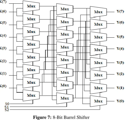
F. Barrel Shifter
[image:4.595.308.550.584.833.2]Shifters are employed in the digital circuits to delay the input. There are different types of combinational shifters such as Funnel, Barrel, Rotational shifters etc. Barrel shifter is based on combinational logic where there are n-inputs and n-outputs with m select lines. Barrel shifters are used in many applications such as DSP.
Figure 6: 8 x 8-bit Reduced
International Journal of Innovative Technology and Exploring Engineering (IJITEE) ISSN: 2278-3075, Volume-8 Issue-8 June, 2019
The most common form of Barrel shifters is multiplexer based Barrel shifters, where output of one multiplexer is fed as input to the next multiplexer depending on the shift distance. Figure 7 illustrates 8-bit multiplexer based Barrel shifter. The number of shifts depends on the select line of the multiplexer. The maximum number of shifts that can happen is seven, since the number of select line is three.
G. Adiabatic Logic
[image:5.595.51.289.336.564.2]Adiabatic logic is a technique that is implemented for low power circuits where minimizing the power dissipation is an important criterion. The term adiabatic means that the energy in the circuit is not dissipated to the ground, it is recycled back to the circuit [10]. AL is a promising low power technique which is efficient in minimizing the power dissipation in the circuit but increases the complexity. Compared to other low power techniques, AL promises to be an efficient low power technique. AL should follow two principles in the design of circuits. One, if there is potential difference between source and a drain, a transistor should never be turned on and the other is if there is a current flowing through the circuit, transistor should be never turned off [11].
Figure 7: 8-Bit Barrel Shifter
The switching power dissipation in static CMOS circuits with capacitive load has a lower limit of 0.5CVDD2 where VDD and C are the supply voltage and capacitive load respectively [19]. This power dissipation can be minimized by using AL. The energy dissipated is supplied through a constant current source in an AL when considering the charge, which is provided by,
2
V T
RC (4)
where,
E: energy dissipated, R: on resistance
C: Load capacitance, T: charging/discharging time, and V is the voltage of the power clock or power supply
The equation (4) infers that if the charging time „T‟ is large, the energy dissipation is minimum or almost zero. But practically, zero dissipation is not possible as it is not possible to provide infinite charging time. The energy dissipation is less in the adiabatic circuit than the static
CMOS circuit if T >> 2RC. The charge stored in the capacitor is recycled by the power clock in the adiabatic logic by which the power dissipation is minimized.
Adiabatic circuits can be quasi/partial adiabatic and full adiabatic family. In case of full adiabatic circuits, the complete charge is recovered back to the circuit, but it is difficult to implement due to the complexity of the circuit. Partial charge is recovered back to the circuit in case of quasi adiabatic circuits and it is easier to implement than the full adiabatic circuits. Quasi/partial AL circuits are less complex than fully AL circuits and dissipates less power compared to static CMOS based circuits.
[image:5.595.313.543.346.484.2]PFAL is an efficient partial/quasi adiabatic technique as compared to other adiabatic techniques, in minimizing the power dissipation. The PFAL circuits consist of a latch made up of two pMOS and nMOS that avoids degradation in the logic level on the output nodes out and /out as illustrated in Figure 8. The F n-tree and /F n-tree indicate the functional blocks which are placed in parallel with PMOS transistors. The „pwr‟ indicates the power clock which minimizes the power dissipation in the circuit. Another advantage of adiabatic logic is that a single circuit provides two outputs, PFAL based inverter circuit provides the output of inverter at out and output of buffer at /out.
Figure 8: Basic Positive Feedback Adiabatic Logic Structure
Figure 9: Simulated Power Clock
There are four intervals in each power clock and a total of four phases of power clocks, where each phase leads the preceding phase by 90 degrees as shown in Figure 9 implemented and simulated in Cadence Virtuoso and Spectre. The power clock is responsible for the charge recovery in adiabatic circuits. The four intervals of the power clock are Evaluate
[image:5.595.310.553.508.661.2]input signal is used to evaluate the output in the E interval. The output is provided to the next stage as input by keeping it stable in the H interval. R interval provides the recovery of energy and symmetry is provided in the W interval.
The power clock at each stage of the circuit is different. If the power clock at the first stage is φ1, then the power clock at the second stage is φ2, which leads φ1 by 90 degrees. The four phases of the power clock are applied to four stages of the circuit, and then the same power clock is repeated to the succeeding stages. The design of adiabatic circuit is such that output of one stage is provided as input to the next stage and each stage has a different power clock. Buffers are used in the absence of circuit to propagate the output of one stage to the next stage, to ensure that all the outputs appear in the same stage.
IV.DESIGNANDIMPLEMENTATIONOFDIRCT FORM FIRFILTER
Schematic of the SQRT CSLA using BEC, RCWTM and Barrel shifter are designed and integrated to form FIR filter using both static CMOS and PFAL in Cadence Virtuoso 180 nm technology and are simulated in Spectre simulator. Sizing of pMOS and nMOS transistors are necessary in static CMOS logic to have equal rise and fall times, as pMOS is slower than nMOS transistor. Based on the DC analysis for a 180 nm CMOS technology, the width of pMOS transistor is set to be 2.75 times of nMOS to obtain symmetrical rise time and fall times. For CMOS circuits, power supply is a DC voltage of 1.8 V and the inputs switch between 0 V and 1.8 V. In case of PFAL circuits, the power supply is a pulsed power clock that switches between 0 V and 1.8 V. The rise time and fall time of the power clock is equal to 25% of the period and the pulse width is also 25% of the period. The input to the adders is a pulse with the pulse width equal to 50% of the period. The output is also a pulse with rise time and fall time equal to 25% of the period as the outputs depend on the power clock.
Different power clocks are used at each stage and hence the output of the adder is displayed in a particular phase depending on the application of power clock.
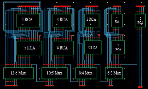
A 16-bit SQRT CSLA using RCA designed using static CMOS logic in Cadence Virtuoso is illustrated in Figure 10. It consists of two stages of RCAs, the first stage considers CIN=„0‟ and the second stage of RCAs have CIN=„1‟, the input to both the stages of RCAs are the same 16-bit inputs. The third stage of SQRT CSLA consists of multiplexers which act as a decision device in selecting the outputs.
The multiplexer selects the output of first stage if the select line S=„0‟ and the output of second stage if the select line S=„1‟. The multiplexer selects the appropriate output. The SQRT CSLA reduces the delay in the circuit as compared to the RCA. The SQRT CSLA using BEC has the same architecture as that of SQRT CSLA using RCA, except that the second stage of RCAs are replaced by BECs. The 16-bit SQRT CSLA using BEC designed using static CMOS logic in Cadence Virtuoso is as depicted in the Figure 11 and the PFAL based SQRT CSLA realized using BEC is shown in Figure 12. The RCWTM designed using static CMOS logic is represented in Figure 13. The partial products are initially multiplied by using AND gates. The
[image:6.595.308.549.97.241.2]WTM groups three rows of partial products into a single group and uses the carry save addition mechanism to add the partial products.
Figure 10: Snapshot of CMOS based 16-Bit SQRT CSLA using
[image:6.595.307.550.277.427.2]RCA
Figure 11: Snapshot of CMOS based 16-Bit SQRT CSLA using
[image:6.595.307.549.456.614.2]BEC
Figure 12: Snapshot of PFAL based 16-Bit SQRT CSLA using
International Journal of Innovative Technology and Exploring Engineering (IJITEE) ISSN: 2278-3075, Volume-8 Issue-8 June, 2019
Figure 13: Snapshot of CMOS based 16-Bit RCWTM
FAs are used where there are three inputs and HAs are used where there are two inputs. The adders use the carry save addition mechanism, so they act as CSAs. The partial products at the final stage are added using the RCA [20]. The RCWTM uses less number of HAs than the WTM and therefore reduces the area and power of the multiplier. The RCWTM designed using PFAL, schematic is not included because size of the image is large.
A Barrel shifter is used as delay element. Barrel shifter is designed using both static CMOS logic and PFAL as per Figure 7. Snapshot of the shifter is not included in the paper. Multiplexers are cascaded to form the shifter. The number of shifts depends on the select inputs. The right shift Barrel shifter shifts the inputs to the right and the left shift Barrel shifter shifts the input bits to the left.
[image:7.595.46.292.552.715.2]A 4-tap FIR filter is realized first by integrating the SQRT CSLA using BEC, RCWTM and Barrel shifter using both static CMOS logic and PFAL in Cadence Virtuoso. After analyzing the outputs, the circuit is scaled up to implement 8-tap FIR filter in both static CMOS and PFAL. The power clocks are provided to the FIR filter by analyzing the stages, inputs and the outputs. The 8-tap PFAL based FIR filter (Top view) implemented in Cadence Virtuoso is as shown in Figure 14. Result analysis of both static CMOS and PFAL based circuits along with power dissipated are discussed in next section.
Figure 14: Snapshot of direct form-I PFAL based 8-Tap FIR
Filter
V. RESULTS AND DISCUSSIONS
The adder, multiplier and shifter architectures are designed in Cadence Virtuoso 180 nm technology and simulated in Spectre simulator. The SQRT CSLA working is verified by providing various combinations of Binary inputs. For illustrations few combinations of inputs are applied. The output of 16-bit SQRT CSLA is
“11000000100001000” for the Binary inputs
“1011001001110011” and “1100111010010101”. Working of RCWTM is verified by providing various combinations of inputs. For instance, when inputs to the RCWTM are “11001110” and “11010011”, output of multiplier is “1010100111001010”. The Barrel shifter is verified by providing various inputs. When the input to the Barrel shifter is “10011011” and select input is “110”, the output is “11100110”. The output is shifted by 6-bits to the left depending on the select inputs.
The inputs to the 8-tap FIR filter are x(n) = “11010011” and coefficients a0=a1=a2=a3= “00000001” and the output is y(n)=“0000001001100111”. The output of an 8-tap FIR filter is y(n)=“0000010011111011” which is
equal to 16-bits for coefficients
a0=a1=a2=a3=a4=a5=a6=a7= “00000001” and inputs x(n)=“11010011”. The outputs of circuits designed using static CMOS logic is displayed in the first phase whereas the output of the PFAL circuits is displayed in different phases due to use of various power clocks. The output waveforms are not presented in the paper.
The static CMOS based 16-bit SQRT CSLA using RCA and 16-bit SQRT CSLA using BEC are simulated in Spectre at different frequencies and the values are listed in Table I. from Table I it can be inferred that the power dissipation increases with the increase in frequency and SQRT CSLA using BEC dissipates less power as compared to SQRT CSLA using RCA. This proves that SQRT CSLA using BEC is a more efficient design w.r.t. power and area. Figure 15 compares the power dissipation of the CSLA using BEC with uniform sized blocks in [12] and the proposed 16-bit SQRT CSLA using BEC with unequal sized blocks at 250 MHz. Table II provides the comparison of power dissipation of the 16-bit SQRT CSLA using RCA and SQRT CSLA using BEC using both static CMOS logic and PFAL at 1 MHz frequency.
Table I: Power Analysis of Static CMOS based SQRT CSLA at
Various Frequencies
Frequency (Hz)
Power Dissipation (µW)
16-Bit SQRT CSLA using RCA
16-Bit SQRT CSLA using BEC
1 K 45.93 22.85
10 K 46.1 22.97
100 K 47.7 24.43
1 M 63.94 38.46
50 M 576.7 216.2
100 M 627.1 316.2
Figure 15: Power Dissipation of static CMOS based CSLA using BEC at 250 MHz
From Table II it can be inferred that, the SQRT CSLA using BEC dissipates less power than the SQRT CSLA using RCA, the BEC uses less number of gates than the full adder. The static CMOS based RCWTM is simulated in Spectre at different frequencies and the dissipated power is as listed in Table III.
Table IV provides the comparison of power dissipation of the WTM in [21] and the proposed RCWTM. It is evident that the power dissipation is 42% less in the proposed RCWTM as compared to the WTM in [21]. The WTM in [21] is designed using compressors which use more number of gates than the conventional FA and HA which contributes to the increase in power dissipation of the circuit. The number of adders in the RCWTM is less with the use of minimum number of HAs with only a small increase in the number of FAs. The total number of gates in the RCWTM has reduced by 12.5%, number of HAs by 52.94% and increasing the number of FAs by 2%. RCWTM reduces the complexity of the circuit by employing minimum number of HAs thereby reducing the area of the multiplier circuit. The PFAL based RCWTM dissipates 81.03% less power as compared to the static CMOS logic based design.
Table II: Power Dissipation of CMOS and PFAL based SQRT
CSLA using RCA and BEC at 1 MHz
Adder Architectures
Power Dissipation in CMOS Logic
(µW)
Power Dissipation in
PFAL (µW)
16-bit SQRT CSLA
using RCA 63.94 19.7
16-bit SQRT CSLA
using BEC 38.46 9.27
Table III: Power Analysis of CMOS based RCWTM at Various
Frequencies
Frequency (Hz)
Power Dissipation of 8 X 8 RCWTM (µW)
1 K 22.62
100 K 29.60
1 M 61.9
50 M 667.6
100 M 1854
250 M 5591
Table IV: Power Analysis of WTM at 250 MHz
Multiplier Architectures Power Dissipation (mW)
8 x 8 WTM [21] 9.64
Proposed 8 x 8 RCWTM 5.591
The left shift Barrel shifter is simulated at different frequencies and dissipated power is depicted in Table V. The right shifter Barrel shifter has also been analyzed. Dissipated power of the right shift Barrel shifter is same as that of the left Barrel shifter. The Figure 16 illustrates the power dissipation of Barrel shifter implemented using both static CMOS logic and PFAL at 1 MHz. The PFAL based Barrel shifter dissipates 97.6% less power compared to static CMOS based Barrel shifter.
[image:8.595.307.551.283.552.2]The CMOS and PFAL based SQRT CSLA using BEC, RCWTM and Barrel Shifter are integrated to form FIR filter implemented using CMOS and PFAL logic. The power dissipation of 8-tap FIR filter is as shown Figure 17.
Table V: Power Analysis of CMOS based left shift Barrel Shifter
at Different Frequencies
Frequency (Hz)
Power Dissipation (µW)
1 K 15.12
10 K 15.32
100 K 16.81
1 M 17.34
50 M 83.33
100 M 991.7
[image:8.595.307.552.585.740.2]250 M 2201
Figure 16: Power dissipation of static CMOS and PFAL based
[image:8.595.77.257.649.746.2]Barrel Shifter
Figure 17: Power Dissipation of static CMOS and PFAL based
International Journal of Innovative Technology and Exploring Engineering (IJITEE) ISSN: 2278-3075, Volume-8 Issue-8 June, 2019
The 8-tap PFAL based FIR filter dissipates 83.4% less power as compared to CMOS based FIR filter. The circuits designed using PFAL are efficient w.r.t. power dissipation with a trade off in terms of complexity and area, compared to static CMOS based circuits.
VI. CONCLUSIONSANDFUTURESCOPE Power optimization is an important criterion in the circuit design, although area and delay have their own prominence. FIR filter is an important element in the DSP systems. The 8-tap direct-form FIR filter is realized by integrating the adders, multipliers and shifters. The power dissipation and area of the SQRT CSLA using RCA is minimized by replacing the RCAs in the second stage by BECs. RCWTM has minimum number of adders as compared to the WTM which reduces the area of the circuit. The SQRT CSLA using BEC, RCWTM and Barrel shifter are integrated to form FIR filter and realized using both static CMOS logic and PFAL. The FIR filter is implemented in Cadence Virtuoso CMOS in 180 nm technology, simulated in Spectre simulator.
The static CMOS based SQRT CSLA using BEC dissipates 39.84% less power as compared to SQRT CSLA using RCA. The PFAL based SQRT CSLA using RCA dissipates 69.18% less power than the static CMOS design and PFAL based SQRT CSLA using BEC dissipate 75.89% less power as compared to static CMOS design. PFAL based RCWTM dissipates 81.03% less power than the static CMOS design. The PFAL based Barrel shifter has a power dissipation reduction of 97.6% than the static CMOS based design. The 8-tap PFAL based FIR filter has a power reduction of 83.4% than the static CMOS based FIR filter. PFAL proves to be an efficient adiabatic technique in minimizing the power dissipation as compared to the static CMOS design for low frequency applications.
In future the adders and multipliers can be designed for higher number of bits. Other AL families are to be analyzed for high frequency operation. The MAC unit can be constructed by designing the accumulator and using the designed adder and multiplier. Practical FIR filters can be designed by designing floating point multipliers instead of Binary multipliers. The designed circuits can be used in applications ranging from DSP and multimedia applications.
REFERENCES
1. M.S. Sheetal and T. Vigneswaran, “High Speed and Efficient 4-Tap FIR Filter Design using Modified ETA and Multipliers,” International Journal of Engineering and Technology, vol. 6, pp. 2159-2170, 2014.
2. M. Gnanasekaran and M. Manikandan, “Performance of FIR Filter with Wallace Multiplier over FIR Filter with Truncated Multiplier,” International Journal of Computer Science and Engineering Communications, vol. 2, pp. 450-455, 2014.
3. V. Dhandapani, “An Efficient Architecture for Carry Select Adder,” World Journal of Engineering, vol. 14, pp. 1-14, 2017.
4. T. Abhiram, T. Ashwin, B. Sivaprasad, S. Aakash and J.P. Anitha, “Modified Carry Select Adder for Power and Area Reduction,” Proceedings of the International Conference on Circuits, Power and Computing Technologies, pp. 1-8, 2017.
5. B.S. Premananda, M.K. Chandana, K.P. ShreeLakshmi and A.M. Keerthi, “Design of Low Power 8-Bit Carry Select Adder using Adiabatic Logic,” Proceedings of the International Conference on Communication and Signal Processing, pp. 1764-1768, 2017.
6. Mandloi, S. Agrawal, S. Sharma and S. Shrivastava, “High-Speed, Area Efficient VLSI Architecture of Wallace-Tree Multiplier for DSP-Applications,” Proceedings of International Conference on Information, Communication, Instrumentation and Control, pp. 1-5, 2017.
7. M.R. Pillmeier, M.J. Schulte and E.G. Walters, “Design Alternatives for Barrel Shifters,” Technical Report, Department of Computer Science and Engineering, Lehigh University, 2001.
8. Vinay B. Biradar, P.G. Vishwas, C.S. Chetan and Premananda B.S., “Design and Performance Analysis of Modified Unsigned Braun and Signed Baugh-Wooley Multiplier,” Proceedings of International Conference on Electrical, Electronics, Communication, Computer and Optimization Techniques, pp. 1-6, 2017.
9. S. Alam, S.R. Ghimiray and M. Kumar, “Performance Analysis of a 4-Bit Comparator Circuit using Different Adiabatic Logics,” Proceedings of the International Conference on Innovations in Power and Advanced Computing Technologies, pp. 1-5, 2017. 10. S.D. Kumar, H. Thapliyal and A. Mohammad, “FinSAL: A Novel
FinFET based Secure Adiabatic Logic for Energy-Efficient and DPA Resistant IoT Devices,” IEEE Transactions on Computer-Aided Design of Integrated Circuits and Systems, vol. 37, pp. 110-122, 2018.
11. Premananda B.S., Nagesh N. Nazare, Pradeep S. Bhat, and Nayana R.J., “Design and Analysis of Adiabatic Vedic Multipliers,” International Journal of Pure and Applied Mathematics, IJPAM, vol. 119, issue 14d, pp. 59-65, October 2018.
12. N. Mageshwari, N. Sasipriya, and R. Ramya, “Optimization of Area and Power Consumption in Carry Select Adder by using BEC,” International Journal of Advance Research, Ideas and Innovations in Technology, vol. 3, pp. 356-360, 2017.
13. N. Jain and P. Ganesh, “A Comparative Study between Different Types of Adders and Multipliers,” International Journal of Electrical, Electronics and Computer Systems, vol. 4, pp. 1-5, 2016. 14. K.B. Jaiswal, V. Nithish Kumar, P. Seshadri and G.
Lakshminarayanan, “Low Power Wallace Tree Multiplier using Modified Full Adder,” Proceedings of the 3rd International
Conference on Signal Processing, Communication and Networking, pp. 1-4, 2015.
15. S. Chinnapparaj and D.S. Sundareswari, “Incorporation of Reduced Full Adder and Half Adder into Wallace Multiplier and Improved Carry-Save Adder for Digital FIR Filter,” International Journal of Circuits and Systems, vol. 7, pp. 2467-2475, 2016.
16. S. Nowrin, L. Jamal and H.M.H. Babu, “Design of an Optimized Reversible Bidirectional Barrel Shifter,” Proceedings of the IEEE International Symposium on Circuits and Systems, pp. 730-733, 2016.
17. A. Mittal, A. Nandi and D. Yadav, “Comparative Study of 16-Order FIR Filter Design using Different Multiplication Techniques,” Proceedings of the Institution of Engineering and Technology Circuits, Devices and Systems, vol. 11, pp. 196-200, 2017.
18. S. Padmapriya and V.L. Prabha, “Design of a Power Optimal Reversible FIR Filter for Speech Signal Processing,” Proceedings of the IEEE International Conference on Computer Communication and Informatics, pp. 1-6, 2015.
19. D. Patel, S.R.P. Sinha and M. Shree, “Adiabatic Logic Circuits for Low Power VLSI Applications,” International Journal of Science and Research, vol. 5, pp. 1585-1589, 2016.
20. Ganavi M.G., and Premananda B.S., “Design of Low Power Square Root Carry Select Adder and Wallace Tree Multiplier using Adiabatic Logic”, Proceedings of the International Conference on Emerging Research in Electronics, Computer Science and Technology, Lecture Notes in Electrical Engineering, vol. 545, Springer, pp. 767-781, 2018.
Notes on contributors
Dr. Premananda B.S. is associated with RV College of Engineering, Bengaluru, India. He is working as Associate Professor in the Department of Telecommunication Engineering. His main areas of interests are in the field of ASIC/FPGA, Low power VLSI, Signal processing, Speech enhancement, Networking and Communication. He has published several research papers on this area in international conferences and journals and guides many projects in his area of research.