Abstract: In many DSP applications, generally multipliers and adders are two key components which are highly complex and consume more power. Out of that the design of adder circuitry is quite complex compared to multiplier which consumes more power. Hence optimization of power consumption of adder circuits is a challenging task in the recent year and is a need of today’s world. In order to give a justice to this problem, work presented in this paper describes the technique of designing floating point adder and subtractor using low power pipelining technique which leads to a reduction in power consumption by a significant amount. Moreover, the presented work in the paper deals with the design of low power transistorized architecture for 32-bit floating point adder/ subtractor without and with pipelining approach in 50nm CMOS VLSI technology. The experimental results demonstrated that, the dynamic power consumption of the floating point adder/subtractor architectures is reduced significantly by employing pipelining technique as compared to the without pipelining technique. Also, in this work a significant improvement has been achieved in the critical path for pipelined approach compared to without pipeline approach. The proposed design is a full custom design prepared and analyzed using cadence 6.15 tool.
Index Terms: Subtractor, Floating Point Adder, Adder/Subtractor Area, Critical path.
I. INTRODUCTION
The current trend towards low-power design is mainly driven by two forces, the growing demand for long-life autonomous portable equipment and the technological limitations of high-performance VLSI systems [1]. For the first category of products, low-power is the major goal for which speed and dynamic range might have to be sacrificed. High speed and high integration density are the objectives for the second application category, which has experienced a dramatic increase of heat dissipation that is now reaching a fundamental limit. These two forces are now merging together as portable equipment grows to encompass high throughput computationally intensive products such as portable computers and cellular phones.
Now-a-days, out of speed, area, time, the low power is the extreme development in the electronic semiconductor industry primary issue in electronic structure frameworks.
Revised Manuscript Received on August 05, 2019.
First Author Dr. Shrikant J. Honade, Department of E & TC, G H Raisoni CEM, Amravati, Maharashtra, India.
Additional power expending results in components overheating and makes the system disappointment. The design of the module will relies upon the lower power dissipation or utilization in any basic arithmetic circuits or segments [2]. Low-power is a basic prerequisite for compact sight and multimedia devices utilizing different signal processing algorithms and architectures [1]. Inexact chips are littler, quicker and devour less energy. Albeit fixed point arithmetic circuits have been examined regarding inexact processing; floating point (FP) arithmetic circuits are altogether more power hungry and they have not been completely considered for inexact computing [10]. Addition is one of the four essential operations in arithmetic. Binary Signed-Digit Residue Number System (BSD-RNS) is one of the explicit and optimized number system. In this paper we propose three low power configuration structures for three BSD-RNS adders [3]. Another structure of superset adder is presented. In this Current Mode approach is proposed for the circuit [4]. With a ton of new ternary circuits being proposed as an option in contrast to the digital logic, we make a stride further to structure a Ternary coded Decimal (TCD) adder circuit dependent on CMOS technology [5]. Redundant Binary Signed Digit (RBSD) number system spurs the designers to design fast processing device. RBSD adders can perform quick addition of two numbers because of the wonder of the nonappearance of carry calculation and manipulation requirement [6]. In present day nanotechnology and quantum calculation, reversible logic plays a significant job as it has insignificant effect on physical entropy. The key purpose of reversible computing is that the electric charge at the output of any circuit ought to stay accessible for further calculations. It implies transistor should not pursue the process of flow of charge during on/off positions [7]. Quantum-dot cell automata (QCA) is a developing field coupled nanotechnology that is made of cells containing electrons [8]. Hybrid logic approach is assumed to design the full adder [9]. Carry select adder (CSLA) is known to be the quickest adder among the customary adder structures [12]. 8-bit, 16-bit, 32-bit, and 64-bit square-root CSLA (SQRT CSLA) have been designed and contrasted with the conventional SQRT CSLA design [16]. Reversible logic has developed as a noteworthy area of research because of its capacity to lessen the power dissipation which is the fundamental necessity in the low power design [14]. The layout design of the ripple carry adder is simple and it makes the calculation to be quicker [13].
Low Power 32-Bit Floating Point
Adder/Subtractor Design using 50nm CMOS
VLSI Technology
In floating point addition (or subtraction), the two numbers must have same exponent for their mantissas to be included (or subtracted) effectively. So in the adder/subtractor unit, the exponent of the smallest number is augmented in such a way that mantissa of both the are equivalent and the mantissa of the smallest number is then moved right 'n' times where 'n' is the difference between the larger and smaller number. After the addition/subtraction task is played out, the resultant mantissa is normalized by the LOD technique. The LOD detects the most significant '1' by tallying the quantity of zeros (nz) before the most significant '1'. The mantissa is then moved left 'nz' times [17]. Advances in CMOS technology have prompted a restored enthusiasm for the design of essential functional units for digital systems [18]. This wide usage space makes the adders a genuine precedent investigation to investigate the design methodologies [18]. Low-power VLSI circuits designs has turned into a vital execution objective in view of the quickly developing technology in versatile mobile computation and communication [19]. Customary design strategies for majority gate are not valuable here because of equipment wasteful aspects [19]. Floating point adders are additionally utilized in encryption and hashing function execution [20].
The speed of a VLSI adder relies upon a few components: technology, circuit family, adder topology, transistor sizes, and second-order effects. Therefore there are no basic principles to be connected while evaluating delay. Skilled designers are prepared to do tweaking the structure to acquire the best execution and most minimal vitality through transistor sizing. But, it is an ad-hoc process and thus it is troublesome, if certainly feasible, to foresee the best topology [21]. The architectures explained by some of the authors used the concept of pipelining and parallel processing in order to improve the performance; which is restricted by the availability of hardware resource on FPGA development platform. Hence, there is a need for full custom VLSI architectures to be designed and developed using CAD VLSI design tool adopting pipelining and parallel processing for implementation in real time applications. Pipelining
transformation results in a reduction in
the critical path, which may be exploited either to extend the clock speed or to cut back power consumption at identical speed. [22].
II. FLOATING POINT ARITHMETICS The IEEE 754-2008 standard specifies however binary floating point numbers are represented additionally as a way to perform arithmetic operations on them [16], [17]. Single precision floating point binary
numbers comprises 32 bits; 1 sign bit, 8 bits for exponent and 23 bits for mantissa. The exponent is represented in
excess-127 code to facilitate exponent
comparison required when performing arithmetic operations. The 23 bit mantissa truly incorporates a 24th implied bit. The floating point number is alleged to be normalized once it’s adjusted such that the implied bit is “1’. Hence it’s dropped upon storage permitting enhanced accuracy and
retrieved when performing operations for
correct calculations. For numbers that are smaller than the smallest normalized number, the implied bit is ‘0’ and also the number is referred to as a de-normalized or subnorm number. Various parallel architectures used for
decimal floating point multipliers are proposed in the literature and the designs were optimized at different levels of the design but it was based on fixed point multiplier [3]. But, due to the developments in the VLSI technology, several complex algorithms that appeared unfeasible to implement into practice, have turn into easily realizable today with preferred concert parameters so that latest designs can be integrated. The performance of system’ is essentially predicted with the capability of the functioning of adder and multiplier [19]. In floating point numbers, multiplication of 2 numbers is basically performed through adding their exponents and multiplying their mantissas. As mentioned before, for floating pont multiplication, the bottle neck of the design is that the 24*24 bit multiplier used to calculate the resulting 48 bit mantissa.
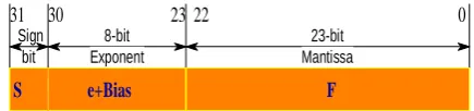
In this work, the single precision numbers in the binary IEEE 754 standard is used. The single precision numbers in the binary IEEE standard are created as shown in Figure 1. The most significant bit is the sign bit, which indicates a negative number if it is set to 1. The following field denotes the exponent with a constant bias added to it as shown in figure 1, the remaining part of the number is normalized to have one non-zero bit to the left of the floating point.
Sign bit
8-bit Exponent
23-bit Mantissa
0 30
31 23 22
e+Bias F
[image:2.595.320.538.341.392.2]S
Figure 1: Standard IEEE Floating Point Number Format Therefore, the value given by the standard format can be expressed using expression (1) [10].
(1)
The range of single precision floating point number varies from
.
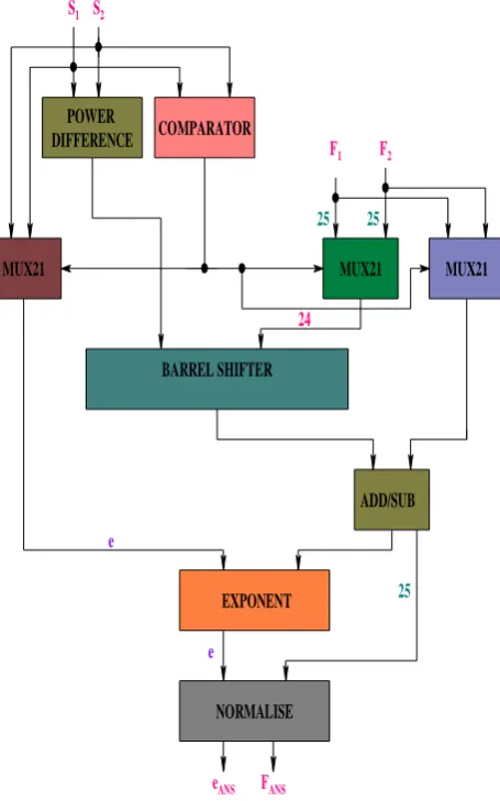
III. FLOATING POINT ADDITION / SUBTRACTION Digital addition operation plays an important role in recent embedded processors and the performance of adder unit basically decides the performance of ALU in CPU and GPU. A composite DSP system consists of a number of adders and multipliers. The performance of such complex system is completely depends upon the efficient design of adders and multipliers. Out of that the most fundamental component is the adders which are incredibly often present inside the building blocks of various systems like controllers and processing chips, FIR filtering, communication, and cryptography etc [22]. Figure 2 illustrated the design process of the floating point addition and subtraction.
S2
S1
F1 F2
25 25
25
eANS FANS
24
e e
COMPARATOR
MUX21 MUX21
BARREL SHIFTER MUX21
ADD/SUB
EXPONENT
NORMALISE POWER
[image:3.595.54.282.227.592.2]DIFFERENCE
Figure 2: Floating Point Addition/Subtraction Unit
Let and represent two floating point numbers;
represents the addition of both number; and
can be rewritten as
= + ( ). The subtraction process is converted to
addition form by inversing the sign bit of F2. For this reason, only addition algorithm is elaborated here. Addition and subtraction algorithms are realized in three steps. Xi represents the number; Si is the sign, ei is exponent and Fi is the fraction part of any number. Lets define the inputs as X1=(S1,e1 ,F1) and A2=(S2,e2,F2). The result is represented as FANS = (SANS,eANS ,fANS)= X1+X2 or X1 + (- X2) The algorithm steps are as follows [23]:
Step 1: If absolute value of X1 is smaller than X2, X1 and X2 are interchanged. The right shift amount of F2 is calculated by subtracting e1 from e2. (Sign)_1_ (Mantissa) is added to the bits after the sign bit (1.F1) or (1.F2).
Step 2: (1.F1) is shifted to the right by the amount of (e1- e2). If the sign bits are equal, then (1.F1) and (1.F2) are added, if not (1.F2) is subtracted from (1.F1). The sign of the resulting number SANS is the sign of the bigger F number.
Step 3: FANS is shifted to the left until the first bit becomes _1_, and amount of the shift is calculated. eANS is obtained by subtracting the amount of shift from e1.
IV. DESIGN METHODOLOGY
The main aim of this work is to design the prototype 32-bit floating point adder/subtractor unit using low power VLSI design strategy at circuit level using industry standard tool like cadence. The various steps used for designing the proposed work is discussed in this section.
A. Designing of Arithmetic Circuits using Front End VLSI Approach
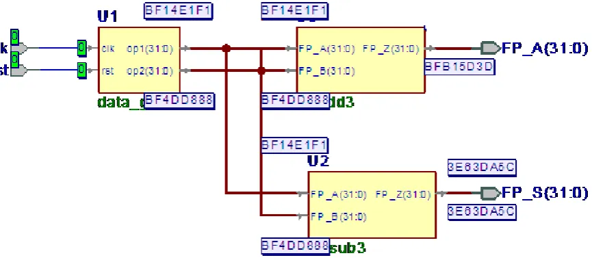
The VLSI front end design involves transformation of the given entity followed by the behavioural and functional simulation based on requirement of the design under consideration. This approach is responsible for creating the register transfer level (RTL) design which is a gate level design. The VHDL RTL models are validated through simulation by means of a number of test benches written in VHDL.
Figure 4: Simulation setup for floating point arithmetic units library ieee;
use ieee.std_logic_1... use ieee.std_logic_a... Design Unit Header
mux_sel <= EXP_diff(8); Statement_1
mw_I13din0 <= A_EXP; Statement_2
mw_I13din1 <= B_EXP; Statement_3
EXP_in(7:0) EXP_out(7:0) SIG_in(SIG_width - 1:0)SIG_out(SIG_width - 1:0)
EXP_in(7:0) EXP_out(7:0) SIG_in(SIG_width - 1:0)SIG_out(SIG_width - 1:0) EXP_in(7:0) EXP_out(7:0)
SIG_in(SIG_width:0)SIG_out(SIG_width - 1:0)
A_in(width - 1:0) A_out(width - 1:0) B_in(width - 1:0) B_out(width - 1:0) invert_A invert_B A_in(width - 1:0) A_out(width - 1:0)
B_in(width - 1:0) B_out(width - 1:0) swap_AB
A_in(28:0) A_out(28:0) B_in(28:0) B_out(28:0) cin diff(8:0)
a_exp_in <= "0" & A_EXP; block_370 FP(31:0) EXP(7:0) isDN isINF isNaN isZ SIG(31:0) SIGN
I3combo : process (a_exp... variable m... variable m... variable diff variable b... begin
mw_I3t0 := mw_I3t1 := borrow := ... diff := sign... A_in <= "00" & A_SIG(23...
block_358
I4combo : process (a_inv,... variable m... variable m... variable m... variable m... begin
mw_I4t0 := mw_I4t1 := mw_I4carry mw_I4sum
cin_sub <= (A_isDN or A_... block_216
eb3_truth_process : proc...
begin
if (A_isNaN isINF_tab isNaN <= isZ_tab ... elsif (B_is... isINF_tab isNaN <= isZ_tab ...
InvertLogic_truth_process : begin
if (A_SIGN invert_A ... invert_B ... elsif (A_SI... invert_A ... invert_B ... elsif (A_SI... invert_A ...
SignLogic_truth_process : variable b... begin
b1_A_SIG... case b1_A... when"000"
OV <= '0'
Z_SIGN when"001"
OV <= '1'
ADD_SUB <= '1'; block_212
B_XSIGN <= not (B_SIGN block_423
b_exp_in <= "0" & B_EXP; block_374 FP(31:0) EXP(7:0) isDN isINF isNaN isZ SIG(31:0) SIGN
B_in <= "00" & B_SIG(23...
block_362
I13combo : process (mw_... variable dt... begin
case mux... when'0' | dtemp :... when'1' | dtemp :... whenoth...
dtemp :...
EXP_isINF <= '1'when (OV block_366 EXP_in(7:0) EXP_out(7:0) SIG_in(27:0) SIG_out(27:0) zero EXP(7:0) FP(31:0) isINF isNaN isZ SIG(22:0) SIGN Z_SIG <= SIG_norm2(25...
block_221 I10 FPround I11 FPnormalize I12 FPselComplement I14 FPinvert I5 FPswap I6 FPalign I0 UnpackFP I1 UnpackFP block_406 or2 block_404 or2 I8 FPadd_normalize FP_A(31:0) FP_B(31:0) I2 PackFP FP_Z(31:0) block_408 or2
library ieee; use ieee.std_logic_1... use ieee.std_logic_a... Design Unit Header
mux_sel <= EXP_diff (8); Statement_1
mw_I13din0 <= A_EXP; Statement_2
mw_I13din1 <= B_EXP; Statement_3
EXP_in(7:0) EXP_out(7:0) SIG_in(SIG_width - 1:0)SIG_out(SIG_width - 1:0)
EXP_in(7:0) EXP_out(7:0) SIG_in(SIG_width - 1:0)SIG_out(SIG_width - 1:0) EXP_in(7:0) EXP_out(7:0)
SIG_in(SIG_width:0)SIG_out(SIG_width - 1:0)
A_in(width - 1:0) A_out(width - 1:0) B_in(width - 1:0) B_out(width - 1:0) invert_A invert_B A_in(width - 1:0) A_out(width - 1:0)
B_in(width - 1:0) B_out(width - 1:0) swap_AB
A_in(28:0) A_out(28:0) B_in(28:0) B_out(28:0) cin diff(8:0)
a_exp_in <= "0" & A_EXP ; block_370 FP(31:0) EXP(7:0) isDN isINF isNaN isZ SIG(31:0) SIGN
I3combo : process ( a_exp... variable m... variable m... variable diff variable b... begin mw_I3t0 := mw_I3t1 := borrow := ... diff := sign... A_in <= "00" & A_SIG(23... block_358
I4combo : process ( a_inv,... variable m... variable m... variable m... variable m... begin mw_I4t0 := mw_I4t1 := mw_I4carry mw_I4sum
cin_sub <= ( A_isDN or A_... block_216
eb3_truth_process : proc... begin if (A_isNaN isINF_tab isNaN <= isZ_tab ... elsif (B_is... isINF_tab isNaN <= isZ_tab ...
InvertLogic_truth_process : begin if (A_SIGN invert_A ... invert_B ... elsif (A_SI ... invert_A ... invert_B ... elsif (A_SI ... invert_A ...
SignLogic_truth_process : variable b... begin b1_A_SIG ... case b1_A... when"000" OV <= '0' Z_SIGN when"001" OV <= '1'
ADD_SUB <= '0'; block_212
B_XSIGN <= not (B_SIGN block_423
b_exp_in <= "0" & B_EXP ; block_374 FP(31:0) EXP(7:0) isDN isINF isNaN isZ SIG(31:0) SIGN
B_in <= "00" & B_SIG(23... block_362
I13combo : process ( mw_... variable dt... begin case mux... when'0' | dtemp :... when'1' | dtemp :... whenoth... dtemp :...
EXP_isINF <= '1'when (OV block_366 EXP_in(7:0) EXP_out(7:0) SIG_in(27:0) SIG_out(27:0) zero EXP(7:0)FP(31:0) isINF isNaN isZ SIG(22:0) SIGN
[image:5.595.50.569.53.628.2]Z_SIG <= SIG_norm2(25... block_221 I10 FPround I11 FPnormalize I12 FPselComplement I14 FPinvert I5 FPswap I6 FPalign I0 UnpackFP I1 UnpackFP block_406 or2 block_404 or2 I8 FPadd_normalize FP_A(31:0) FP_B(31:0) I2 PackFP FP_Z(31:0) block_408 or2
[image:5.595.51.568.420.629.2]Figure 6: RTL view of 32-bit floating point subtractor
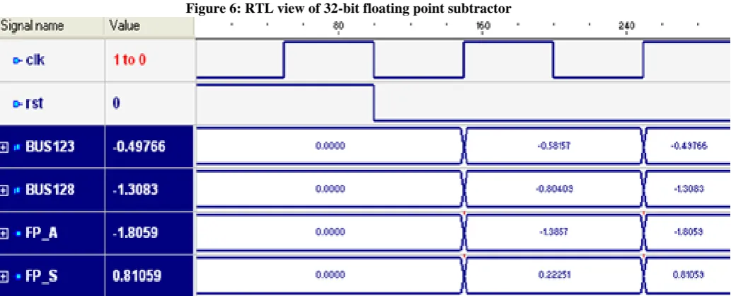
Figure 7: Simulation result of floating point arithmetic unit
B. Designing of Arithmetic Circuits using Back End VLSI Approach
In this step, all the above designed floating point arithmetic units are mapped to the transistor level and then tested it using cadence 6.15 tool.
B.1 Floating Point Adder using 50nm CMOS technology
[image:6.595.48.553.168.509.2]Here, the above designed floating point adder unit is passed through cadence 6.15 rtl compiler tool. It will map the front end designs into gate level net-list i.e. it will transfer the high level language design into basic gate and then it is synthesized in order to obtain the transistorized designs for 32-bit floating point adder, is obtained using 50nm technology. Then in order to check the functionality of the design, simulation setup or test setup is prepared using cadence 6.15 virtuoso tool as shown in figure 8. This setup consists of data generator and the floating point adder unit.
Figure 8: Simulation setup for floating point adder
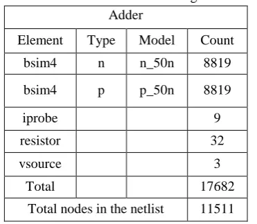
Figure 9: Simulation result of floating point adder The synthesis report showing transistor count of the circuit as
[image:6.595.74.260.575.737.2]depicted in table 1.
Table 1. Element Count for Floating Point Adder Adder
Element Type Model Count
bsim4 n n_50n 8819
bsim4 p p_50n 8819
iprobe 9
resistor 32
vsource 3
Total 17682
Total nodes in the netlist 11511
The simulation is performed using cadence 6.15 ADE tool in ultrasim mode. The simulation result along with the output waveform is shown in figure 9. From simulation result, we can easily visualize that after applying two operands op11 & op22, the circuit is able to perform addition of two as represented by ‘y’ and it is matching with the front end result shown in figure 7.
From table 1, it is clear that, the total number of bsim4 transistors required for designing the floating point adder is 17634 excluding the encrypted models. Also, the power analysis is done for the above circuit which results into average power consumption of 0.000381 watt when operated on input supply voltage of 1volt.
B.2 Floating Point Subtractor using 50nm CMOS technology
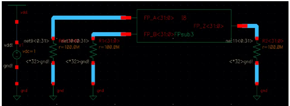
6.15 rtl compiler tool and then it is synthesized in order to obtain the transistorized designs for 32-bit floating point adder, is obtained using 50nm technology. After that, to check the functionality of the design, simulation setup or test setup is prepared using cadence 6.15 virtuoso tool as shown in figure 11. This setup consists of data generator and the floating point adder unit.
[image:7.595.65.536.337.466.2]Figure 11: Simulation setup for floating point subtractor The simulation result along with the output current waveform is shown in figure 12.
Figure 12: Simulation output for floating point subtractor
From simulation result, we can easily visualize that after applying two operands op11 & op22, the circuit is able to perform subtraction of two as represented by ‘y’ and it is matching with the front end result shown in figure 7. The synthesis report is
[image:7.595.77.271.571.722.2]basically netlist showing transistor count of the circuit as depicted in table 2.
Table 2. Element Count for Floating Point Subtractor Subtractor
Element Type Model Count
bsim4 n n_50n 8863
bsim4 p p_50n 8863
iprobe 9
resistor 32
vsource 3
Total 17770
Total nodes in the netlist 11583
From the table 2, it is clear that, the total number of bsim4 transistors required for designing the floating point multiplier is 17726 excluding the encrypted models. Also, the power analysis is done for the above circuit which results into average power consumption of 0.0005404watt when operated on input supply voltage of 1volt.
The design of pipelined floating point adder/subtractor circuit is done here by using two approaches i.e. front end and back end. Front end approach is related with the coding and simulation whereas the backend is related with transforming the design to the transistor level and resembling the functionality with front end approach. The proposed design is a full-custom design. Also, pipelined arithmetic unit requires the triggering circuits for their operation in order to achieve high performance; control unit is designed by using FSM approach. During the process, several times online IEEE floating point calculator and MATLAB tool is used for data conversion and verification. Also, some times synthesizable and non-synthesizable code style is also used for accurate representation. In this step, ripple carry floating point
adder/subtractor is redesigned using the concept of pipelining in order to optimize the power. Figure 13 shows the RTL view for 32-bit pipelined floating point adder/subtractor and multiplier unit. The simulation outputs is illustrated in figure 14 for pipelined floating point adder/subtractor respectively, wherein FP_A and FP_B represents the two floating point number randomly generated using data generator, clk indicates clock signal and FP_Z, represents the corresponding output signal. The simulation output shows that, the output FP_Z approximately takes 9 clock cycles to update the output in case of adder/subtractor. The result in these cases is self explanatory and more precise also. In figure 14, ADD_SUB is a multiplexed signal which performs addition operation when ADD_SUB=1 and subtraction operation when ADD_SUB=0.
library ieee; use ieee.std_logic_1... use ieee.std_logic_a... Design Unit Headerclk
A _ EX P(7 :0 ) A _ alig n(28 :0 )
A _ in(2 8:0 ) A _ SIG N_ stage 2
A _ isINF B _ alig n(28 :0 )
A _ isNaN B _ XS IGN_ stage 2
A _ isZ cin
A _ S IG N E X P_ b ase _stag e 2(7 :0 )
A DD_ S UB _ out inve rt_ A
B _ EX P(7 :0 ) inve rt_ B
B _ in(2 8:0 ) isINF_ tab_ stag e 2
B _ isINF isNaN_ stag e 2
B _ isNaN isZ_tab _stag e 2
B _ isZ
B _ XS IG N
cin_ sub
clk
E X P _d iff(8:0 )
A _ alig n(28 :0 ) A _ SIG N_ stage 3
A _ SIG N_ stage 2 ad d _o ut(2 8:0 )
B _ alig n(28 :0 ) B _ XS IGN_ stage 3
B _ XS IGN_ stage 2 E X P _b ase (7:0 )
cin isINF_ tab_ stag e 3
clk isNaN_ stag e 3
E X P_ b ase _stag e 2(7 :0 ) isZ_tab _stag e 3
inve rt_ A
inve rt_ B
isINF_ tab_ stag e 2
isNaN_ stag e 2
isZ_tab _stag e 2 A DD_S UB A _ EX P(7 :0 )
clk A _ in(2 8:0 )
FP _ A(3 1:0 ) A _ isINF
FP _ B(3 1:0 ) A _ isNaN
A _ isZ
A _ S IG N
A DD_ S UB _ out
B _ EX P(7 :0 )
B _ in(2 8:0 )
B _ isINF
B _ isNaN
B _ isZ
B _ XS IG N
cin_ sub
E X P _d iff(8:0 )
A _ SIG N_ stage 3 E X P _no rm(7:0 )
ad d _o ut(2 8:0 ) isINF_ tab_ stag e 4
B _ XS IGN_ stage 3 isNaN_ stag e 4
clk isZ_tab _stag e 4
E X P _b ase (7:0 ) O V _ stage 4
isINF_ tab_ stag e 3 S IG _no rm(2 7:0 )
isNaN_ stag e 3 Z_ S IG N_stag e 4
isZ_tab _stag e 3 ze ro _ stage 4
clk isINF_ tab
E X P _no rm(7:0 ) isNaN
isINF_ tab_ stag e 4 isZ_ tab
isNaN_ stag e 4 O V
isZ_tab _stag e 4 S IG _no rm2 (2 7:0 )
O V _ stage 4 Z_ E XP (7:0 )
S IG _no rm(2 7:0 ) Z_ S IG N
Z_ S IG N_stag e 4 ze ro
ze ro _ stage 4
clk FP _ Z(3 1:0 )
isINF_ tab
isNaN
isZ_ tab
O V
S IG _no rm2 (2 7:0 )
Z_ E XP (7:0 )
Z_ S IG N
ze ro I2
FPadd_stage2
I3
FPadd_stage3 I1
FPadd_stage1
I4
FPadd_stage4 ADD_SUB
clk
I5
FPadd_stage5
I6
FPadd_stage6 FP_A(31:0)
FP_B(31:0)
[image:8.595.70.556.255.822.2]FP_Z(31:0)
Figure 13: RTL view of pipelined floating point adder/subtractor
Figure 14: Simulation output of pipelined floating point adder/subtractor
[image:8.595.52.543.273.548.2]The transistorized designs for 32-bit pipelined ripple carry floating point adder/subtractor are developed in 50nm technology.
Figure 15: Simulation setup for pipelined floating point adder/subtractor The synthesized designs of pipelined floating point
adder/subtractor unit in stages are obtained which is basically a transistorized network consisting of pmos and nmos transistors designed using 50nm technology. Then in order to check the functionality of the design, simulation setup or test setup is prepared using cadence 6.15 virtuoso tool as shown in figure 15. This setup consists of data generator and the
[image:9.595.46.548.482.676.2]floating point adder unit. The simulation is performed using cadence 6.15 ADE tool in ultrasim mode. The simulation result is shown in figure 16. From simulation result, we can easily visualize that after applying two operands op11 & op22, the circuit is able to perform required arithmetic operating on the applied signal as represented by ‘add_op’. The synthesis report is depicted in table 3.
Table 3. Element Count for Pipelined Floating Point Adder/subtractor
Pipelined Adder/subtractor
Element Type Model Count
bsim4 n n_50n 8911
bsim4 p p_50n 8911
iprobe 12
resistor 32
vsource 66
Total 17932
Total nodes in the netlist 11857
From the table 3, it is clear that, the total number of bsim4 transistors required for designing the pipelined floating arithmetic unit is 17822 excluding the encrypted models. Also, the power analysis is done for the above circuit which results into average power consumption of 0.00000027watt when operated on input supply voltage of 1volt. The results shown in figure 16 are in hexadecimal format which are same as that of front end result depicted in figure 14 when verified using hex2float converter designed manually
V. EXPERIMENTAL RESULTS
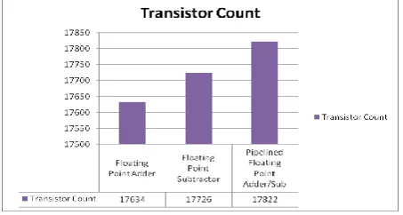
The universal gates like NAND, NOR and basic gates are accessible as customary standard cells. These cells accessible within the library are used to synthesize the design. During this work Cadence 6.15 design library is manually employed for synthesizing the rest of the design. The experimental results obtained are compared in terms of performance metric like transistor count, power consumption and critical path is discussed. Critical path is nothing but the path between input node and output node with maximum delay. Because of this the computational speed of the circuit gets reduced. So, in order to obtain the computational speed, the value of critical path should be as low as possible. Similarly, the power consumption of the circuit should be as low as possible for the low power devices and the pipelining technique is one which can be used to reduced the power consumption at circuit level [22]. Hence pipelining technique is used in this work for power optimization and the obtained results are outstanding. Figure 17 (a) and figure 17(b) shows the transistor count and required for implementation of floating point adder/subtractor without and with pipelining technique.
Figure 17 (a) : Transistor count
Figure 17 (b): Area occupied
Figure 18: Power consumption
[image:10.595.62.285.66.221.2]The power consumption and critical path comparison for the ripple carry adder/subtractor designed using pipeling approach and without pipelined approach is illustrated in figure 18 and figure 19 respectively. Also, the detailed performance comparison of different floating point adder/subtractor is depicted n table 4. From all these results, it can be easily observed that, the performance of proposed 32-bit ripple carry pipelined adder/subtractor is superior as compared to non-pipelined in terms of power consumption and critical path.
[image:10.595.310.545.541.636.2] [image:10.595.56.283.607.728.2]VI. CONCLUSION
In this paper an novel 32-bit ripple carry floating point adder/subtractor unit is successfully designed using backend 50nm CMOS VLSI technology and its functionality is also verified using front end approach. From the experimental results it is clear that by using the concept of pipelining, the power consumption of the adder/subtractor unit is found to be 0.27 miliwatt which is very less as compared to the non-pipelined architectures. Moreover a critical path for the pipelined architecture is found as 55 i.e. delay is less in pipelined architecture as compared to simple. Apart from this, an area comparison for pipelined and simple floating point adder/subtractor unit is demonstrated which represents that the pipelined units required some more area as compared to non- pipelined unit. Hence in future research, there is a scope to put efforts in order to minimize both power and area combinely. Also, one may go for designing the layout for the proposed arithmetic circuits for the fabrication of chip.
VII. ACKNOWLEDGEMENT
[image:11.595.61.542.331.796.2]The author sincerely thanks to Guru Dr. Prashant V. Ingole, Chairman IETE Amravati centre, Professor & Head, Department of Information Technology, PRMITR, Badnera(M.S.) for their constant guidance and supervision in completing this work. The author also thanks to his mentor and beloved principal of GHRCEM Amravati, Dr. Vijay Rathod, and Dr. S. V. Dudul, Head of Applied Electronics department, SGBAU Amravati for their valuable suggestion, criticism and time to time encouragement in carrying out this research. Last but not the least, author also expresses his warm appreciation to his Brother, Amol, Mr. Nitin A. Shelke for their constant help in editing this article.
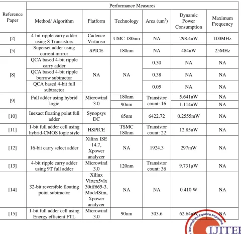
Table 4. Detail performance comparison of various floating point adders/subtractor
Reference Paper
Performance Measures
Method/ Algorithm Platform Technology Area (um2)
Dynamic Power Consumption
Maximum Frequency
[2] 4-bit ripple carry adder using 8 Transistors
Cadence
Virtuoso UMC 180nm NA 298.4uW 100MHz
[5] Superset adder using
current mirror SPICE 180nm NA 484uW 25MHz
[8]
QCA based 4-bit ripple carry adder
NA NA
0.30 NA NA
QCA based 4-bit ripple
borrow subtractor 0.38 NA NA
QCA based 4-bit full
subtractor 0.05 NA NA
[9] Full adder using hybrid logic
Microwind 3.0
180nm Transistor
count: 16
5.641uW NA
90nm 1.114uW NA
[10] Inexact floating point full adder
Synopsys
DC 65nm 6422.72 0.2555mW NA
[11] 1-bit full adder cell using
hybrid-CMOS logic style HSPICE
TSMC 180nm
Transistor
count: 22 12.85uW NA
[12] 16-bit carry select adder
Xilinx ISE 14.7, Xpower analyzer
NA 1924.3 297mW NA
[13] 4-bit ripple carry adder using 9T full adder
Microwind
3.0 120nm
Transistor
count: 36 9.731μW NA
[14] 32-bit reversible floating point subtractor
Xilinx Virtex5vlx 30tff665-3, ModelSim, Xpower analyzer
NA NA 0.410 W NA
[15] 1-bit full adder cell using Energy efficient FTL
Microwind
[16]
8-bit Modified SQRT CSLA architecture
Cadence rtl compler, encounter
180nm
895 188.4uW NA
16-bit Modified SQRT
CSLA architecture 1,929 471.8uW NA
32-bit Modified SQRT
CSLA architecture 3,985 969.9uW NA
64-bit Modified SQRT
CSLA architecture 8,183 2050.1uW NA
[19] Low power and high
performance full adder HSPICE 180nm NA
3.961uW 100MHz 2.545uW 0.9616uW 0.53103uW [20]
32-bit Ling adder using
Lander Fischer Synopsys
DC 180nm
11038 NA
NA 32-bit Ling adder using
Kogge-Stone 13561 NA
Proposed work
32-bit ripple carry flaoting point adder
Cadence Virtuoso
NCSU 50 nm
44.085 0.318 mW,
vdd=1V
500MHz 32-bit ripple carry
flaoting point subtractor 44.315
0.5404 mW, vdd=1V
32-bit pipelined ripple carry flaoting point
adder/subtractor
44.555 0.27 uW,
vdd=1V
REFERENCES
1. Arunraj R. and Vishnu Narayanan P M, “Design of Robust and Power
Efficient Full Adder Using Energy Efficient Feed through Logic,” International Journal of Engineering Research and General Science, vol. 2, no. 2, pp. 96–101, 2014.amlesh Pedraj and Jayendra kumar, “Design and Implementation of Low Power Inexact Floating Point Adder,” International journal of Computer Application, vol. 168, no.7, pp. 43–46, 2017.
2. Sudhakar Alluri, M. Dasharatha, B. R. Naik, and N. S. S. Reddy,
“Design of Low Power High Speed Full Adder Cell with XOR/XNOR Logic Gates,” International Conference on Communication and Signal Processing, IEEE, pp. 565–570, 2016.
3. Adib Armand and Somayeh Timarchi, “Low power design of binary
signed digit residue number system adder,” 2016 24th IEEE Iranian Conference on Electrical Engineering (ICEE), pp. 844–848, 2016.
4. S. A. H. Ejtahed and M. B. Ghaznavi-Ghoushchi, “Design and
Implementation of a Power and Area Optimized Reconfigurable Superset Parallel Prefix Adder,” 24th Iranian Conference on Electrical Engineering (ICEE), IEEE, pp. 1655–1660, 2016
5. J. Mounika, Mohd Ziauddin Jahangir and K. Ramanujam, “CMOS
based design and simulation of Ternary Full Adder and Ternary coded decimal (TCD) adder circuit,” 2016 International Conference on Circuit, Power and Computing Technologies [ICCPCT], IEEE, pp. 1–5, 2016.
6. Vandana Shukla, O. P. Singh, G. R. Mishra, and R. K. Tiwari, “A
novel approach to design a redundant binary signed digit adder cell using reversible logic gates,” 2015 IEEE UP Section Conference on Electrical Computer and Electronics (UPCON 2015), pp. 1-6,2015.
7. Varun Pratap Singh and Manish Rai, “Verilog design of full adder
based on reversible gates,” Proceeding International Conference on Advanced Computer Communication and Automation (ICACCA 2016), IEEE, pp. 1–5, 2016.
8. C. Labrado and H. Thapliyal, “Design of adder and subtractor circuits
in majority logic-based field-coupled QCA nanocomputing,” Electronics Letter, vol. 52, no. 6, pp. 464–466, 2016.
9. M. Nikhil Theja and T. Balakumaran, “Energy efficient low power
high speed full adder design using hybrid logic,” 2016 International Conference on Circuit, Power Computer Technology, pp. 1–8, 2016.
10. Weiqiang Liu, Libnin Chen, C. Wang, Maire O. Neill, and F.
Lombardi, “Design and analysis of inexact floating-point adders,” IEEE Transactions on Computer, vol. 65, no. 1, pp. 308–314, 2015.
11. Milad Jalalian Abbasi morad, S. R. Talebiyan, and E. Pakniyat,
“Design of New Low Power High-performance Full Adder with New XOR-XNOR Circuit,” Second International Congress on Technology, Communication and Knowledge (ICTCK 2015), pp. 153–158, 2015.
12. M. Vinod Kumar Naik and Y. M. Aneesh, “Design of carry select
adder for low-power and high speed VLSI applications,” Proceeding of 2015 IEEE International Conference on Electrical, Computer Communication Technology (ICECCT 2015), pp. 1-4, 2015.
13. S. Usha and T. Ravi, “Design of 4 bit ripple carry adder using hybrid
9TFull Adder,” 2015 International Conference on Circuit, Power Computer. Technology [ICCPCT], IEEE, pp. 1–8, 2015.
14. AV Anantha Lakshmi and GF Sudha, “Design of a reversible single
precision floating point subtractor,” Springerplus open journal, vol. 3, no. 1, pp. 1-20, 2014.
15. B. Ramkumar and H. M. Kittur, “Low-power and area-efficient carry
select adder,” IEEE Transactions on very large scale integration (VLSI) systems, vol. 20, no. 2, pp. 371–375, 2012.
16. Lamiaa S. A. Hamid, Khaled A. Shehata, Hassan El-Ghitani, and
Mohamed ElSaid, “Design of generic floating point multiplier and adder/subtractor units,” 2010 12th International conference on computer modelling and simulation, IEEE computer society, pp. 615–618, 2010.
17. Bart R. Zeydel, Dursun Baran, and Vojin G. Oklobdzija,
“Energy-efficient design methodologies: high-performance VLSI adders,” IEEE Journal of Solid-State Circuits, vol. 45, no. 6, pp. 1220–1233, 2010.
18. Mohammad Hossein Moaiyeri, Reza F. Mirzaee, and Keivan Navi,
“Two new low-power and high-performance full adders,” Journal of Computers, vol. 4, no. 2, pp. 119–126, 2009.
19. Giorgos Dimitrakopoulos and Dimitris Nikolos, “High-speed
parallel-prefix VLSI ling adders,” IEEE Transactions on Computers, vol. 54, no. 2, pp. 225–231, 2005.
20. Vojin G. Oklobdzija, Bart R. Zeydel, Hoang Q. Dao, Sanu Mathew,
and R. Krishnamurthy, “Comparison of high-performance VLSI adders in the energy-delay space,” IEEE Transactions on very large scale integration (VLSI) systems, vol. 13, no. 6, pp. 754–758, 2005.
21. Keshab K. Parahi, "VLSI Digital Signal Processing System: Design
and Implementation," Wiley Inter-science publication, John Wiley and Sons Inc. PP.1-784.
22. Ujwal S. Ghate, Ajay A. Gurjar, Vilas N. Ghate, “ Power Optimization
of single precision FFTdesign using fully combinational circuits,” 15th International Conference on
Advanced Computing
AUTHORS PROFILE