i
SINGLE MOLECULE ELECTRONICS IN IONIC LIQUID
MEDIA
Thesis submitted in accordance with the requirements of the University Of Liverpool for the degree of Doctor in Philosophy
by
Nicola Julie Kay
ii
Abstract
iii
Acknowledgements
I would first of all like to offer my greatest appreciation and thanks to my supervisor Professor Richard Nichols for his patience, support and advice throughout my research. I would also like to thank my secondary supervisor Professor Simon Higgins and Professor Don Bethell for useful discussion and advice, especially during group meetings.
Much appreciation must go to the rest of the Nichols/Higgins group, both past and present, with special mention going to Dr. Wolfgang Haiss and Dr. Edmund Leary for the inspiration for this research and useful discussion. Finally, Dr. Gita Sedghi, whose help and support I could not have done without.
I would like to offer my gratitude to our collaborators in this project, Professor Walther Schwarzacher of Bristol University, Professor Bing-Wei Mao of Xiamen University, China, and Professor Jens Ulstrup of the Danish Technical University, Denmark. Special thanks to the Ulstrup group in the DTU for being so welcoming and helpful during my visit in September 2010.
On a personal note, I would like to thank all my friends and family, including those who are no longer with us, for their support during my PhD. A special mention must go to my Grandad George for always being so supportive and enthusiastic during my studies.
iv
Contents
Abstract ... ii
Acknowledgements ... iii
Contents ... iv
List Of Figures ... vii
List Of Tables ... xvii
1 Introduction ... 2
1.1 A History Of Single Molecule Electronics ... 2
1.1.1 Benzenedithiol... 3
1.1.2 Model System: Alkanedithiols ... 4
1.1.3 Redox-Active Systems: Molecular Switches ... 6
1.1.4 Single Molecule Devices... 12
1.1.5 Room Temperature Ionic Liquids In Electrochemistry ... 13
1.2 Cyclic Voltammetry ... 16
1.2.1 Cyclic Voltammetry And Surface Reactions ... 19
1.3 The History Of STM ... 21
1.3.1 Quantum Tunnelling ... 22
1.4 STM In Single Molecule Electronics ... 24
1.4.1 Electron Transport ... 24
v
1.4.3 Superexchange ... 26
1.4.4 Simmons Model ... 26
1.4.5 Double Barrier Tunnelling ... 28
1.4.6 Resonant Tunnelling ... 29
1.4.7 Kuznetsov-Ulstrup Electron Transfer Model ... 30
1.4.8 Marcus Theory ... 32
1.4.9 Non-Coherent Transport: Hopping ... 34
1.4.10 Metal-Molecule Contacts ... 36
1.4.11 Conductance Groups ... 38
1.5 STM Techniques ... 38
1.5.1 STM-I(s) ... 39
1.5.2 STM Controlled Break-Junction ... 41
1.5.3 Electrochemical In-situ STM ... 42
1.6 References ... 43
2 Conductance Measurements Of Alkanedithiols In A Room Temperature Ionic Liquid ... 56
2.1 Introduction ... 56
2.2 Aim ... 58
2.3 Experimental Methods ... 59
2.4 Results And Discussion ... 60
vi
2.6 References ... 75
3 The Electrochemistry Of Pyrrolo-Tetrathiafulvalene ... 80
3.1 Introduction ... 80
3.2 Aim ... 81
3.3 Experimental Methods ... 81
3.4 Results And Discussion ... 82
3.4.1 Confirmation Of The Cyclic Voltammetry Of Leary et al. ... 82
3.4.2 Pyrrolo-TTF In A Room Temperature Ionic Liquid ... 87
3.5 Conclusions ... 100
3.6 References ... 100
4 Conductance Measurements Of Pyrrolo-Tetrathiafulvalene In A Room Temperature Ionic Liquid ... 105
4.1 Introduction ... 105
4.2 Aim ... 107
4.3 Experimental Methods ... 108
4.4 Results And Discussion ... 109
4.5 Conclusions ... 121
4.6 References ... 122
5 Conclusions ... 127
6 Appendix ... 131
vii
6.2 Polarisation Modulation Infrared Reflection Adsorption Spectroscopy ... 139
6.3 Gold-On-Glass Substrate ... 143
6.4 References ... 143
6.5 Publications ... 144
List Of Figures
Figure 1: A theoretical molecular rectifier TTF-TCNQ designed by Aviram and Ratner.9 ... 3
Figure 2: Benzenedithiol, the first molecule to have its conductance quantitatively measured. It is also the subject of several conflicting results. ... 4
Figure 3: (A) the electron transfer between (A0) and (B+) and (B) the mechanism proposed describing the operation of the system. First of all, the TTF moiety in (A0) where the switch is in the “off” position, is oxidised, creating (A+). Due to
electrostatic repulsion, the crown ether rotates leading to the creation of (B+) where the TTF+ is located outside the cyclophane. (B0) where the switch is in the “on” position, is formed when the bias voltage is returned to 0 V. In order to regenerate (A0) thus closing the switch, a bias of +2 V must be applied. “Off” refers to a lower conductance state for the molecular film, while “on” refers to a higher conductance state. Figure taken from reference 30. ... 6
Figure 4: The three inorganic transition metal complexes studied by Albrecht et al. They were adsorbed on either a Au(111) or a Pt(111) substrate.31-34 ... 7
Figure 5: Cyclic voltammetry for compounds (A), (B) and (C), referred to in Figure 4, at various scan rates. Figure adapted from reference 32. ... 8
viii
Figure 7: Structure of the redox-active molecule pyrrolo-tetrathiafulvalene (PTTF). ... 11
Figure 8: Conductance vs. overpotential plots of (a) viologen, (b) PTTF and (c) 6Ph6, where Ph refers to a phenylene group. Viologen exhibits a broad on-off transition as the potential is swept through the equilibrium potential of the molecule. PTTF has a sharp off-on-off switching behaviour at the redox potential, which is predicted by the KU model. 6Ph6 is redox-inactive so as expected, the conductance isn’t affected by changes in potential. Figure taken from reference 47. ... 11
Figure 9: Cyclic voltammetry of the Os bisterpyridine complex (Ossac) assembled on Au(111) in the aqueous electrolyte HClO4 (black) and in the RTIL BMIPF6 (red).
The wider potential window accessible using the RTIL is clear at potentials greater than approximately +0.3 V. Figure taken from reference 57. ... 14
Figure 10: Potential waveform of a cyclic voltammogram. Potential is swept linearly between V1 and V2 over time. ... 16
Figure 11: A simple 3-electrode electrochemical cell connected to a potentiostat. .. 17
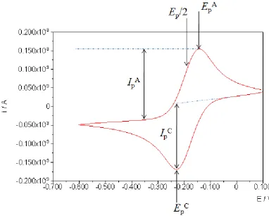
Figure 12: Example cyclic voltammogram showing the anodic peak potential (EpA),
anodic peak current (IpA), cathodic peak potential (EpC), cathodic peak current (IpC)
and the half peak potential (Ep/2). ... 18
Figure 13: Example of a cyclic voltammogram of the redox reaction of an ideal species adsorbed on the working electrode. ... 19
Figure 14: Cyclic voltammograms of a Au(111) surface in a H2SO4 electrolyte. The
butterfly peak is contained in the black box and has been enlarged. This occurs due to the adsorption of sulfate anions. Figure adapted from reference 69. ... 20
ix
Figure 16: Quantum tunnelling through a potential barrier. In the tip and surface, the energy of the electron (E) is greater than the potential (V). However, in the gap between the electrodes, the potential is larger than the energy of the electron so the electron is forbidden to be located in this region according to classical mechanics. However, quantum mechanics allows the electron to “tunnel” through the gap, as the probability of the electronic wavefunction being present across the gap is > 0. ... 22
Figure 17: Current-distance plot demonstrating the current exponential decay as the STM tip is withdrawn from the substrate surface. This plot was taken in a BMIOTf medium, the STM tip was Au wire and the substrate was a gold-on-glass substrate. The decay constant for this plot is -11.69 nm-1.. ... 24
Figure 18: Non-resonant coherent superexchange tunnelling through a molecular bridge. In the superexchange tunnelling mechanism, the electron transfer is aided by the molecular orbital despite its large distance from the Fermi levels of the metallic contacts. ... 26
Figure 19: Representation of the Simmons model, describing direct tunnelling. The original Simmons model rectangular barrier is shown in green. When image charge is taken into account, the potential barrier is reduced in height and rounded (red). Since the Simmons model employs rectangular barriers, the effective height and width of the potential barrier are used (blue). This representation is not to scale. ... 28
Figure 20: Resonant tunnelling through a molecular bridge. The electron tunnels via a molecular orbital which results in an increase in conductance compared to direct tunnelling where the molecular orbitals do not aid tunnelling to such an extent. ... 29
Figure 21: A plot of conductance vs. sample potential, showing the conductance increase at the redox potential of the molecular wire, a feature of resonant tunnelling. ... 30
Figure 22:Adiabatic two-step electron transfer with partial vibrational relaxation. The electron tunnels to the LUMO, which then relaxes in energy after being reduced. The electron vacates the LUMO it reaches the EF of the second electrode. The
x
Figure 23: Energy curves depicting the Marcus Theory of ET. (A) shows the ET in the “normal” region, (B) is “activationless” and (C) is the “inverted” region.121 ... 33
Figure 24: Non-coherent electron hopping through a long molecular wire. Due to the long length of the molecule, it is preferable for the electron to hop from one fragment of the molecule to another, rather than tunnel. Hopping requires thermal activation for the electron to overcome ϕ, the difference in energy between the EF of the tip and
the energy of the receiving molecular fragment. ... 34
Figure 25: Semilog plot of resistance vs. molecular length of conjugated OPI molecular wires. A very distinct change in the length dependence behaviour is observed between OPI 4 and OPI 6 at approximately 4 nm length. This is the change in ET mechanism from coherent tunnelling to non-coherent hopping. Figure taken from references 86, 87... 35
Figure 26: Arrhenius plot conjugated OPI 4, OPI 6 and OPI 10 conjugated molecular wires. The temperature dependence shows an obvious change from OPI 4 to OPI 6 from no dependence to an Arrhenius dependence. This acts as further confirmation of a ET regime change from coherent tunnelling to non-coherent hopping. Figure taken from reference 86. ... 36
Figure 27: The three different conductance groups A (a), B (b) and C (c). The molecule exhibiting a group A conductance is adsorbed on a flat, terraced surface, or connected to a single gold adatom. For a group B conductance, one of the terminal groups is adsorbed at a step edge site whereas both the terminal groups are adsorbed at a step edge when the C group conductance is observed. ... 38
Figure 28: The STM-I(s) technique, which is used to measure the conductance of single molecules. The tip is held above the substrate at a distance dictated by the current setpoint Iset (A). Occasionally, a molecule will spontaneously bridge the gap
between tip and substrate (B). The tip is then retracted from the surface in the z-direction (C). When the molecule is held between the two electrodes, a current plateau is observed on the I(s) scan (blue). As the tip continues to retract, the
xi
Figure 29: A conductance histogram of ODT in ambient conditions, showing one (I), two (II) and three (III) molecules in the junction at ~1 nS, ~2 nS and ~3 nS
respectively. 505 I(s) scans were used to create this histogram. ... 41
Figure 30: The STM-BJ technique used to measure the single molecule conductance of molecular wires. The STM tip is crashed into the substrate surface (B). The tip is then retracted (C) until the bridge of atoms joining the tip and substrate snaps (D). If a molecule bridges the gap, then as with the I(s) technique, a plateau is seen in the current-distance scan. As the tip is retracted further, the molecule breaks off from one of the electrodes, which results in the current dropping sharply. ... 42
Figure 31: A schematic of an in-situ electrochemical STM cell. The STM controller contains a bipotentiostat which allows measurements to be performed under
electrochemical potential control. Four electrodes are contained in the cell; the substrate acts as the working electrode, metal wires are used as the counter and reference electrodes and the STM tip acts as the 4th electrode. The tip must have a protective coating to reduce faradaic currents flowing between the tip and electrolyte. This is known as the leakage current. ... 43
Figure 32: Logarithm of the low conductance group A (blue), medium conductance group B (black) and high conductance group C (red) measured for alkanedithiols in ambient conditions, as a function of the number of CH2 groups (N) at a bias voltage
Vbias = +0.6 V. Figure taken from reference 4. ... 57
Figure 33: Current through ODT as a function of the bias voltage for both the low conductance group A (blue) and the medium conductance group B (black). The solid lines are fits to the Simmons model. Figure taken from reference 4. ... 57
Figure 34: Tunnelling current enhancement when the sample potential is swept as the bias potential is kept constant at +0.7 V. Figure taken from reference 15. ... 58
xii
Figure 36: Conductance histograms of (a) PrDT, (b) PDT, (c) HDT, (d) ODT, (e) NDT, and (f) UDT on Au(111) obtained using the I(s) method; VBIAS = +0.6 V ; I0 =
20 nA ; 500, 501, 500, 538, 578, and 503 scans were analysed respectively. ... 62
Figure 37: Conductance histograms of (a) PrDT, (b) PDT, (c) HDT, (d) ODT, and (e) UDT on Au(111) obtained using the BJ method; VBIAS = +0.6 V ; I0 = 20 nA ;
501, 500, 507, 504, and 505 scans were analysed respectively. ... 63
Figure 38: Example of a 2-D histogram for ODT which shows both the break-off distance and the conductance, obtained using the I(s) method including 538 scans. Both the A conductance group and the “break-off tail” have been labelled. ... 66
Figure 39: 2-D histogram representations of (a) PrDT, (b) PDT, (c) HDT, (d) ODT, (e) NDT, and (f) UDT, obtained using the I(s) method. The A group and break-off decay regions are clearly visible on each plot. The streaking seen on the 2-D
histogram of UDT is due to the large bin sizes required for the very low conductance values... 67
Figure 40: 2-D histograms of (a) PrDT, (b) PDT, (c) HDT, (d) ODT, and (e) UDT, obtained using the STM BJ method. The medium conductance group B is clearly visible on all plots. As the total tip-to-substrate distance s cannot be quantitatively measured, a distance scale bar is instead given for the x-axis showing a distance of 1 nm. ... 68
Figure 41: Logarithm of the low conductance group A (blue) and medium conductance group B (black) as a function of the number of CH2 units in the
polymethylene chain, for alkanedithiols in the ionic liquid BMIOTf; VBIAS = +0.6 V;
I0 = 20 nA. When N > 8, the conductance decays exponentially as a function of
length with a decay factor β ≈ 1 Å-1, as shown on the plot in the dark blue ellipse... 69
Figure 42: Plots of the logarithm of the conductance G versus the length of the alkanedithiol for both the low conductance group A (a) and the medium conductance group B (b). The slope of these plots gives the decay factor β which for both
xiii
Figure 43: A comparison of the logarithm of the conductance versus the number of CH2 units in the polymethylene chain of alkanedithiols measured in air (red) and in
the RTIL BMIOTf (blue). The data for the measurements recorded in air were taken from reference 4. ... 71
Figure 44: The three different conductance groups A (a), B (b) and C (c). The molecule exhibiting a group A conductance is adsorbed on a flat, terraced surface, or connected to a single gold adatom. For a group B conductance, one of the terminal groups is adsorbed at a step edge site whereas both the terminal groups are adsorbed at a step edge when the C group conductance is observed. ... 72
Figure 45: Logarithm of the current flowing through ODT as a function of the bias voltage, for the conductance group A measured in the RTIL BMIOTf. ... 72
Figure 46: Logarithm of the current flowing through ODT as a function of the bias voltage measured using the I(s) method for the low conductance group A. The data collected by Haiss et al. in reference 4 are shown by the blue circles, and the data collected in the RTIL BMIOTf are shown by the gray squares. The solid blue line is the Simmons model fit. ... 73
Figure 47: The two stable, fully-reversible redox reactions of pyrrolo-TTF. The first transition, from the neutral pyrrolo-TTF0 to the radical cation pyrrolo-TTF·+ is visible in aqueous electrolyte, whereas the second transition from the radical cation pyrrolo-TTF·+ to the dication pyrrolo-TTF2+ is not. ... 80
Figure 48: Cyclic voltammograms of pyrrolo-TTF (blue), viologen 6V6 (red) and 6Ph6 (black), where Ph is a phenylene group. The redox peaks are clearly visible for both 6V6 and pyrrolo-TTF. For the latter, the redox peak seen is indicative of the first redox transition from pyrrolo-TTF0 to pyrrolo-TTF·+.2 Figure taken from
reference 2. ... 81
Figure 49: Cyclic voltammogram of a pyrrolo-TTF monolayer on Au(111), in a 10 mM Na2HPO4/NaH2PO4 electrolyte pH = 6.9 with a scan rate of 1 Vs-1. ... 83
xiv
recorded in October 2008. The red scan was recorded in October 2009 using the same procedure. However, no redox peaks are present. ... 84
Figure 51: Mass spectrum of pyrrolo-TTF. The peaks at 598.1 and 599.1 show the molar mass of pyrrolo-TTF, confirming that the molecule has not degraded. Acknowledgements to Jean Ellis and Moya McCarron of the Mass Spectrometry Service in the Department Of Chemistry,University Of Liverpool. ... 86
Figure 52: IR spectrum of a pyrrolo-TTF monolayer on a gold-on-glass slide recorded using PM-IRRAS. The substrate had been immersed for approximately 24 hours before the spectrum was obtained. ... 87
Figure 53: Reaction scheme showing the protonation of the pyrrolo-TTF moiety in the presence of water.5, 6 ... 88
Figure 54: Cyclic voltammograms of (a) 1 mM pyrrolo-TTF in BMIOTf, (b) 1 mM ferrocene and pyrrolo-TTF in BMIOTf and (c) 1 mM pyrrolo-TTF in BMIOTf shown in (a) but the potential scale has been calibrated to the Fc/Fc+ redox couple. The scan rate employed for these voltammograms is 50 mVs-1. ... 89
Figure 55: Cyclic voltammograms of the N-tosylated monopyrrolo-TTF A (bold trace) and monopyrrolo-TTF B (light trace) in acetonitrile. The working and counter electrodes were Pt and the potential scale was calibrated to the Ag/AgCl reference.3 Figure adapted from reference 3. ... 90
Figure 56: Cyclic voltammogram of a 1 mM solution of pyrrolo-TTF in N2 BMIOTf
at different scan rates. ... 91
Figure 57: Cyclic voltammograms of (a) pyrrolo-TTF monolayer on Au(111) in BMIOTf, (b) 1 mM ferrocene in BMIOTf with the pyrrolo-TTF monolayer on Au(111) and (c) pyrrolo-TTF monolayer on Au(111) in BMIOTf shown in (a) but the potential scale has been calibrated to the Fc/Fc+ redox couple. The scan rate
employed for these voltammograms is 50 mVs-1. ... 92
Figure 58: Cyclic voltammogram of a pyrrolo-TTF monolayer on Au(111) in N2
xv
Figure 59: Cyclic voltammograms of (a) a 1 mM solution of pyrrolo-TTF in vacuum dried BMIOTf, (b) 10 mM ferrocene in BMIOTf with 1 mM pyrrolo-TTF and (c) 1 mM solution of pyrrolo-TTF in BMIOTf shown in (a) but the potential scale has been calibrated to the Fc/Fc+ redox couple. The scan rate employed for these
voltammograms is 50 mVs-1. ... 94
Figure 60: Cyclic voltammogram of a 1 mM solution of pyrrolo-TTF in vacuum dried BMIOTf at different scan rates. ... 95
Figure 61: Cyclic voltammograms of (a) a 10 mM solution of pyrrolo-TTF in vacuum dried BMIOTf, (b) 10 mM ferrocene in BMIOTf with 1 mM pyrrolo-TTF and (c) 10 mM solution of pyrrolo-TTF in BMIOTf shown in (a) but the potential scale has been calibrated to the Fc/Fc+ redox couple. The scan rate employed for these voltammograms is 50 mVs-1. ... 95
Figure 62: Cyclic voltammogram of a 10 mM solution of pyrrolo-TTF in vacuum dried BMIOTf at different scan rates. ... 97
Figure 63: Cyclic voltammograms of (a) pyrrolo-TTF monolayer on Au(111) in vacuum dried BMIOTf, (b) 10 mM ferrocene in BMIOTf with the pyrrolo-TTF monolayer on Au(111) and (c) pyrrolo-TTF monolayer on Au(111) in BMIOTf shown in (a) but the potential scale has been calibrated to the Fc/Fc+ redox couple. The scan rate employed for these voltammograms is 50 mVs-1. ... 98
Figure 64: Cyclic voltammogram of a pyrrolo-TTF monolayer in vacuum dried BMIOTf at different scan rates. ... 99
Figure 65: The two stable, fully-reversible redox reactions of pyrrolo-TTF. The first transition, from the neutral pyrrolo-TTF0 to the radical cation pyrrolo-TTF·+ is visible in aqueous electrolyte, whereas the second transition from the radical cation pyrrolo-TTF·+ to the dication pyrrolo-TTF2+ is not. ... 105
xvi
Figure 67: Cyclic voltammetry of pyrrolo-TTF in a solution of N2 dried BMIOTf
(black) and as a monolayer on Au(111) in an electrolyte of N2 dried BMIOTf (red).
Scan rate = 50 mVs-1. ... 106
Figure 68: Examples of I(s) scans of pyrrolo-TTF in BMIOTf at a sample potential of +0.12 V. ... 109
Figure 69: Conductance histograms of pyrroloTTF using sample potentials of (a) -0.6 V, (b) -0.55 V, (c) -0.5 V, (d) -0.45 V, (e) -0.35 V, (f) -0.3 V, (g) -0.25 V, and (h) -0.2 V obtained using the I(s) method; VBIAS = +0.6 V ; I0 = 20 nA ; 100, 102, 500,
101, 501, 100, 503, and 100 scans were analysed respectively. Sample potentials are with respect to the Pt quasi reference. ... 110
Figure 70: Conductance histograms of pyrroloTTF using sample potentials of (i) -0.1 V, (j) -0.05 V, (k) 0 V, (l) 0.05 V, (m) -0.1 V, (n) -0.12 V, (o) -0.15 V, and (p) 0.2 V obtained using the I(s) method; VBIAS = +0.6 V ; I0 = 20 nA ; 500, 105, 500, 100,
100, 501, 110, and 510 scans were analysed respectively. Sample potentials are with respect to the Pt quasi reference. ... 111
Figure 71: Conductance histograms of pyrrolo-TTF using sample potentials of (q) 0.25 V, (r) 0.3 V, (s) 0.4 V, (t) 0.45 V, and (u) 0.5 V, obtained using the I(s) method; VBIAS = +0.6 V ; I0 = 20 nA ; 100, 100, 503, 100, and 100 scans were analysed
respectively. Sample potentials are with respect to the Pt quasi reference. ... 112
Figure 72: 2-D histogram representations of pyrrolo-TTF conductance data at sample potentials of (a) -0.6 V, (b) -0.55 V, (c) -0.5 V, (d) -0.45 V, (e) -0.35 V, (f) -0.3 V, (g) -0.25 V, (h) -0.2 V , (i) -0.1 V, (j) -0.05 V, (k) 0 V, (l) 0.05 V, (m) 0.1 V, (n) 0.12 V, and (o) 0.15 V vs the Pt quasi reference, obtained using the I(s) method. The conductance of pyrrolo-TTF, and break-off decay regions are clearly visible on each plot. ... 114
xvii
Figure 74: (a) Plot of conductance of pyrrolo-TTF against the sample potential and (b) the plot in (a) overlaid with a cyclic voltammogram (blue line) of a pyrrolo-TTF monolayer. The point of maximum conductance corresponds with the redox potential of each redox transition of pyrrolo-TTF. The voltammogram shown here was
recorded in N2 dried BMIOTf. A detailed explanation for this can be found in the
previous chapter. ... 116
Figure 75: Conductance-sample potential relationship of pyrrolo-TTF in the RTIL BMIOTf. The red lines show the long KU model (Equation 4.1), and the blue lines show the simplified KU model (Equation 4.2). For both redox transitions, both KU model variations fit the experimental data well. ... 118
Figure 76: Conductance-overpotential relationship of pyrrolo-TTF in an aqueous buffer electrolyte at pH 6.8, recorded by Leary et al.2 The red line shows the long KU model (Equation 4.1), and the blue line shows the simplified KU model (Equation 4.2). The λreorg of pyrrolo-TTF in an aqueous buffer was estimated as
0.405 eV using the long KU model and 0.43 eV using the simplified KU model. .. 120
List Of Tables
Table 1: Diagnostic tests for cyclic voltammograms of reversible processes. ... 19
Table 2: Table of possible coherent electron transfer mechanisms (adapted from references 19, 82, and 104) ... 25
Table 3: The transmission probabilities of various contact groups. Table adapted from references 88, 89... 37
Table 4: Conductance values for the A and B conductance groups for the
alkanedithiols measured ... 64
xviii
Table 6: Examples of some of the attempts to obtain good quality, reproducible voltammetry of pyrrolo-TTF. The voltammetry of some of these attempts can be found in the Appendix of this thesis. ... 85
Table 7: The difference between the anodic and cathodic peak potentials ΔEp, and the
redox potential E1/2, given as the midpoint of the anodic and cathodic peak; given for
a 1 mM pyrrolo-TTF in N2 dried BMIOTf solution and with ferrocene added. The
average ferrocene E1/2 value is used to calibratethe potential scale. ... 90
Table 8: The difference between the anodic and cathodic peak potentials ΔEp, and the
redox potential E1/2, given as the midpoint of the anodic and cathodic peak; given for
a pyrrolo-TTF monolayer on Au(111) in N2 dried BMIOTf solution and with
ferrocene added. The average ferrocene E1/2 value is used to calibratethe potential
scale. ... 93
Table 9: The difference between the anodic and cathodic peak potentials ΔEp, and the
redox potential E1/2, given as the midpoint of the anodic and cathodic peak; given for
a 10 mM pyrrolo-TTF in vacuum dried BMIOTf solution and with ferrocene added. The average ferrocene E1/2 value is used to calibratethe potential scale. ... 96
Table 10: The difference between the anodic and cathodic peak potentials ΔEp, and
the redox potential E1/2, given as the midpoint of the anodic and cathodic peak; given
for a pyrrolo-TTF monolayer on Au(111) in vacuum dried BMIOTf solution and with ferrocene added. The average ferrocene E1/2 value is used to calibratethe
potential scale. ... 99
Table 11: The break-off distances estimated for pyrrolo-TTF at the sample potentials measured. The sample potentials given are with respect to the Pt quasi reference. 113
Table 12: Values of λreorg, γ, and ξ used in the modelling of both redox transitions of
pyrrolo-TTF using the long KU and simplified KU model of ET. ... 118
Table 13: Values of λreorg, γ, and ξ used in the modelling of pyrrolo-TTF in aqueous
1
Chapter 1
2
1
Introduction
1.1 A History Of Single Molecule Electronics
Over the last sixty years, technology has evolved beyond recognition. The invention of the transistor in 19481, 2 was a pivotal moment in the history of electrical devices. Moore’s Law, developed in 1965 by Intel’s co-founder Gordon Moore, describes how the number of components on an integrated circuit is expected to double approximately every eighteen months.3, 4 As traditional “top-down” methods of manufacturing integrated circuits, such as photolithography5-7 will start to reach their limit in the near future, new methods of creating extremely small components will need to be realised in order to continue this exponential growth of components per chip. Single molecule electronics (SME), in which single molecules could be used as such components, shows ethereal promise due to a single molecule’s small size and functionality.
3
Figure 1: A theoretical molecular rectifier TTF-TCNQ designed by Aviram and Ratner.9
In 1988, Aviram et al. used a scanning tunnelling microscope (STM) to observe the I-V characteristics of an asymmetrical hemiquinone molecule.10 This was the first measurement of its kind, addressing a monolayer between two metallic electrodes. A monolayer was assembled on a Au(111) on mica surface by immersion in a solution containing the hemiquinone molecule, which binds to the Au via the sulfur on the thioether. Measurements were taken using a Pt tip and I-V scans were obtained at several positions on the surface. On flat areas where it is assumed that there are no molecules present, the I-V characteristics were reminiscent of bare Au. However, when a hemiquinone molecule was positioned between the Pt tip and Au substrate, the current peaked at approximately -200 mV when the potential was swept in a negative direction. This abrupt increase in current was however, not observed when the potential was swept in a positive direction. This result in itself is not spectacular, as two different metals were used for the electrodes, which may in itself result in rectification, but the fact that the experiment was performed was a huge leap forward in the field.10, 11
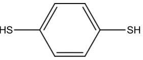
1.1.1 Benzenedithiol
4
Figure 2: Benzenedithiol, the first molecule to have its conductance quantitatively measured. It is also the subject of several conflicting results.
Reed et al. used a mechanically controlled break junction (MCBJ) at room temperature to perform their measurements.12 This was fabricated by adsorbing a monolayer of BDT onto a length of gold wire. This wire was then stretched until finally, breakage occurred, resulting in the formation of two tips of atomic sharpness. These tips were then brought closer together so that a single molecule of BDT bridges the gap. I-V measurements were performed and the conductance of a single molecule was measured to be 45 nS.12 Xiao et al. obtained a conductance of 851 nS for a single molecule of BDT14, which is approximately 20 times larger than Reed et al.’s value. They used their STM controlled break junction (BJ) technique14, 20 which is described in detail in a later section of this thesis. Lörtscher et al. and Martin et al. both used MCBJ in UHV conditions and both obtained different conductance values for BDT, at 3.85 nS and 77 nS respectively.15-17 Lörtscher et al. however found that the conductance of BDT does exhibit a temperature dependence.17 Haiss et al. used the STM I(t) technique to study the effect of molecular tilting on the conductance.18 This involved holding the STM tip at a set distance above the surface and measuring current jumps as molecules spontaneously bridged the gap between tip and substrate. Haiss et al. found that the conductance of BDT increased as the tilt angle increased. An untilted BDT molecule was found to have a conductance of 8.6 nS. This increased significantly when the tilt angle was greater than about 50°.18 Discrepancies between the different research groups could be partly explained by this occurrence. It was also found more recently that different conductance groups exist depending on the nature of the adsorption site.21 This could also help to provide an explanation for the many different conductance values measured for this molecule.
1.1.2 Model System: Alkanedithiols
5
system in single molecule electronics, partly due to their stability and large HOMO-LUMO gap.19, 22
Xu and Tao used their celebrated STM BJ technique to measure the conductance of hexanedithiol (HDT), octanedithiol (ODT) and decanedithiol (DDT), and measured conductance values of about 93 nS, 20 nS and 1.5 nS respectively.20 These measurements demonstrated the exponential dependence of conductance on length for these alkanedithiols. Another important parameter which quantifies the exponential length dependence, specifically how much the current decays per unit length, is the decay factor β, calculated using the equation I = I0exp(-βN) where N is
6
1.1.3 Redox-Active Systems: Molecular Switches
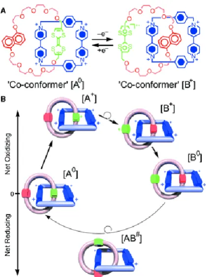
[image:24.595.214.424.309.591.2]Redox-active molecular wires are of considerable interest in the field of SME. They exhibit a switching behaviour when the potential is swept, which changes their redox state, resulting in a jump in conductance. The first reversible redox-active switch studied was a (2)catenane-based system, consisting of two interlocked molecules, one being a crown ether containing a tetrathiafulvalene (TTF) moiety and a 1,5-dioxynaphthalene unit on opposing sides of the molecule, and the other being a cyclophane containing two bypyridinium moieties.30 A Langmuir-Blodgett (LB) film of the catenane was sandwiched between a Ti/Al electrode and a polycrystalline n-Si electrode.
Figure 3: (A) the electron transfer between (A0) and (B+) and (B) the mechanism proposed describing the operation of the system. First of all, the TTF moiety in (A0)
where the switch is in the “off” position, is oxidised, creating (A+). Due to electrostatic repulsion, the crown ether rotates leading to the creation of (B+) where
7
conductance state for the molecular film, while “on” refers to a higher conductance state. Figure taken from reference 30.
In the ground state (A0), the TTF unit is located inside the cyclophane, having a bipyridinium unit on either side. When a bias of -2 V is applied, the TTF is oxidised and a new conformer (B+) is formed as the TTF+ moves outside the cyclophane ring. As the bias is reduced to 0 V, the TTF+ is reduced, forming compound (B0). The conformer will revert back to its ground state when a bias of +2 V is applied. It was determined that the HOMO-LUMO gap for conformer (B0) is smaller than for (A0), which means that the electrical conductance is greater for (B0) than for (A0), meaning that (A0) represents the “switch open” state and (B0) represents the “switch closed” state. This is shown in Figure 3.30 Both oxidation and reduction are essential for device switching, as illustrated by the fact that the compound can only be cycled reproducibly if the opening voltage is greater than 2 V and the closing voltage less than -1.5 V.
Another class of molecular switches are inorganic transition metal complexes, with Os and Co complexes being studied by the Ulstrup group.31-34 They are particularly attractive due to their ease of synthesis, versatility of the ligands, and stability as well as the reproducibility of their switching behaviour. Albrecht et al. have extensively studied three of these compounds.31-34
Figure 4: The three inorganic transition metal complexes studied by Albrecht et al. They were adsorbed on either a Au(111) or a Pt(111) substrate.31-34
(A) (B) (C)
8
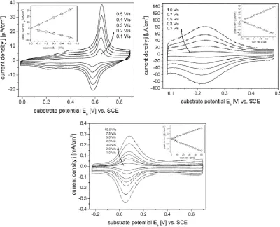
[image:26.595.119.520.147.471.2]The electrochemistry of these compounds was investigated using cyclic voltammetry. Self assembled monolayers (SAMs) were assembled on either Au(111) or Pt(111) substrates.
Figure 5: Cyclic voltammetry for compounds (A), (B) and (C), referred to in Figure 4, at various scan rates. Figure adapted from reference 32.
In all three voltammograms in Figure 5, the redox properties are clearly visible. The peak height Ip increases linearly with scan rate υ which confirms that the compound
is adsorbed onto the electrode surface. The interfacial electron transfer (ET) kinetics of compounds (A) and (B) are much faster than for compound (C).32, 35, 36 In situ scanning tunnelling spectroscopy (STS) was then performed on the compounds. It(Es) spectroscopy with constant bias, where the tunnelling current (It) was measured
as potential (Es) was swept with the feedback loop switched off, showed an increase
9
mechanism of electron tunnelling through these compounds is a two-step process involving vibrational relaxation. This is known as the Kuznetsov-Ulstrup (KU) model and is described in further detail later in this thesis.32-34
Viologens contain a 4,4’-bipyridinium (bipy) functional group and are one of the most widely studied redox-active molecular wires, undergoing a reversible redox reaction at about -0.4 V vs. SCE.37-47
Figure 6: A viologen molecule, containing the bipy moiety. Carbon chains of varying lengths can be attached to either end of the moiety and are thiol-terminated,
allowing for the molecule to be adsorbed onto a Au substrate. R = (CH2)n
Theoretically, ET through viologen should proceed via the KU model.38, 39, 41, 42, 44, 46,
47 However, this is now known not to be the case. Haiss et al. developed the STM
I(s) technique for measuring single molecule conductance on a viologen molecule, specifically 6-(1’-(6-mercapto-hexyl)-(4,4’)bipyridinium)-hexane-1-thiol, using EC in situ STM. They observed a conductance change from about 0.5 nS to 2.8 nS, as the molecule was swept through its equilibrium redox potential and switched from its oxidised state to its reduced state. However, a maximum in the tunnelling current was not observed, indicating that the KU ET model is not applicable in this instance.40
10
of viologen junctions. It was found that by using this same technique for the monothiolated viologen monolayer, these current plateaux were not observed, since this molecule lacks a second thiol group to bind to the Au STM tip. The conductance of the dithiolated viologen was measured using the method described above and varying the sample potential (Es) between -0.25 V and -0.75 V, which is where the
first reduction of the viologen moiety takes place, from the dication form to the radical cation form. Similarly to Haiss et al., a plot of tunnelling current vs. sample potential was created and a similar shape was observed, although beyond approximately -0.7 V, the curve acquired by Li et al. levels off. They attribute this minor difference to the difference in electrolyte used and the absence of oxygen, as the experiment by Haiss et al. was performed in ambient conditions whereas the experiment performed by Li et al. was under an argon atmosphere.40, 46 Li et al. then went on to study asymmetric viologen junctions using a monothiolated viologen, which was assembled on the Au STM tip. A setpoint current of 100 pA was applied and with a constant bias of +0.1 V, the tip potential was swept and I-V curves were recorded between -0.15 V and -0.65 V with a scan rate of 2.0 Vs-1. An average of twenty scans were plotted and the resulting curve is reminiscent of the KU model, with a maximum tunnelling current close to the equilibrium redox potential of the first reduction. Only a small number of viologen molecules situated on the apex of the STM tip are believed to contribute to this tunnelling current, as the tunnelling current decreases exponentially with distance. As the tip potential approaches the equilibrium redox potential, the LUMO of the viologen approaches the Fermi energy of the substrate, initiating the first step of the two-step ET, hence the maximum in the tunnelling current.46
11
adsorbed molecules are not attached to the STM tip and are instead separated from it by the electrolyte solution. Nevertheless, the data obtained suggests that this model of ET prevails.42
Pyrrolo-tetrathiafulvalenes (PTTF) are particularly interesting, as they are stable in three redox states, PTTF0, PTTF+ and PTTF2+. The first of these redox reactions has an equilibrium redox potential within the range where the Au-thiol bond is stable in aqueous electrolyte.47-51
Figure 7: Structure of the redox-active molecule pyrrolo-tetrathiafulvalene (PTTF).
A comparison of the electrochemical and conductance properties of viologen and PTTF was carried out by Leary et al.47 As described earlier, viologen exhibits a
broad off-on transition instead of the sharp off-on-off switching predicted by the KU model.40, 42, 46, 47 I(s) measurements of PTTF were taken under electrochemical potential control, and the conductance vs. electrode potential plots exhibit a maximum in the tunnelling current, reminiscent of the KU model.47
Figure 8: Conductance vs. overpotential plots of (a) viologen, (b) PTTF and (c) 6Ph6, where Ph refers to a phenylene group. Viologen exhibits a broad on-off transition as the potential is swept through the equilibrium potential of the molecule.
PTTF has a sharp off-on-off switching behaviour at the redox potential, which is predicted by the KU model. 6Ph6 is redox-inactive so as expected, the conductance
12
A possible explanation as to why the viologen and PTTF behave differently is that PTTF is planar in both the PTTF0 and PTTF+ redox states, whereas V2+ can be twisted and possibly becomes more coplanar upon reduction, which may have an impact on the ET mechanism.47
1.1.4 Single Molecule Devices
One of the main objectives of the extensive research undertaken in the field of SME is the fabrication of devices containing a single molecule, or arrays of single molecules. This has also turned out to be a major stumbling block in the field. One issue is how to connect each individual molecule in a device to the metal electrodes; it has proven difficult to reduce the width of a metal wire to the molecular scale, meaning that the advantages of the small size of molecules have not yet been fully realised.52 Current semiconductor technologies have changed the way we live, although they are not without their disadvantages. Presently, as the components in a device get smaller, they suffer from current leakage, which increases power consumption.53 We will also one day in the not too distant future, reach the limit of what the widely used lithography techniques can achieve. Utilising single molecules in such devices could drastically reduce power consumption as well as greatly increase their capacity. However, it has to be said that such ideas are futuristic and it is unclear if they can ever be practically realised. Nevertheless, an integration of molecules within a more conventional semiconductor microelectronics platform is conceivable and may find future application. These may be niche applications, for example array sensing devices.
13
One application in particular which molecular electronics may possibly benefit is information storage or memory. Lindsay and Bocian discussed how porphyrin molecules show potential to be incorporated into data storage devices in the future.54 Porphyrins in particular are relatively simple to synthesise, are customisable, stable and are capable of storing charge, without an applied potential, for several minutes. They typically have two stable redox states, which can be cycled reproducibly for extended periods of time with no degradation, and porphyrin monolayers can survive at high temperatures in an inert atmosphere, which is particularly important during the manufacture of such devices.54 Porphyrin molecules could possibly be incorporated into dynamic random access memory (DRAM), thus creating a hybrid device which utilises existing semiconductor technology with single molecules acting as components. The traditional lithography techniques used to produce DRAM currently suffer the disadvantage that due to the small dimensions of the transistor gate of the widely used “trench/stack” design, the transistor has a leakage current which depletes the charge stored on the capacitor in the storage cell. If single porphyrin molecules could be used as a storage cell, then the amount of data able to be stored per unit area would massively increase, as well as being more energy efficient.54 A hybrid data storage prototype was produced in 2004 by Kuhr et al. which used a porphyrin molecule in conjunction with the existing metal oxide semiconductor technology.54, 55 This prototype was a 1 Mb DRAM chip, consisting of four 256 kbit arrays of the molecular capacitors. One major advantage of these hybrid devices was realised as the charge-storage density was found to be greater or equal to the charge storage density of existing semiconductor devices. This development is not yet viable for practical use as of yet, but it shows a glimpse of the potential of single molecular devices in the future.54, 55 Porphyrins have also shown potential for use in flash memory devices. Shaw et al. integrated a monolayer of a Co porphyrin in a flash memory structure successfully.56 The Co porphyrin demonstrated three reversible redox states which would be particularly useful in flash memory devices.56
1.1.5 Room Temperature Ionic Liquids In Electrochemistry
14
have several advantages over conventional aqueous electrolytes. These include a wider potential window, low volatility and high conductivity.57-61 The wider potential window is of particular interest, as aqueous electrolytes are hindered by hydrogen evolution and surface oxidation at low and high potentials respectively, which may obscure some redox processes. The high conductivity of RTILs means that a carrier electrolyte is not required, which reduces the likelihood of contamination being present in the electrolyte solution.
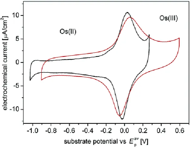
[image:32.595.163.480.325.569.2]The wider potential window enjoyed by ionic liquids has been demonstrated by Albrecht et al. using an Os bisterpyridine complex (Ossac). Cyclic voltammetry was performed on Ossac in both aqueous electrolyte and the RTIL 1-butyl-3-methylimidazolium hexafluorophosphate (BMIPF6).57
Figure 9: Cyclic voltammetry of the Os bisterpyridine complex (Ossac) assembled on Au(111) in the aqueous electrolyte HClO4 (black) and in the RTIL BMIPF6 (red).
The wider potential window accessible using the RTIL is clear at potentials greater than approximately +0.3 V. Figure taken from reference 57.
Albrecht et al. also studied the Ossac system under BMIPF6 using STM. They
15
potential was swept, a larger tunnelling current was observed at positive potentials. The tunnelling current dropped to approximately 0 nA below the cathodic peak potential, which is a demonstration of rectification behaviour. The bias range studied was wider than would have been possible using an aqueous electrolyte, highlighting once more one of the advantages of using RTILs in SME.57
There have in RTILs, been a range of defined electrochemical surface studies of single crystal electrodes, which have addressed issues such as surface etching and reconstruction. Lin et al. monitored the change in the Au(111) surface structure in the RTIL 1-butyl-3-methylimidazolium tetrafluoroborate (BMIBF4) at a range of
potentials using STM.62 It was found that the Au(111) surface undergoes surface restructuring at larger negative potentials greater than approximately -0.9 V. Between -0.9 and -1.2 V, on the terraces, tiny pits of atomic height started to emerge. These pits remained up to approximately – 2.4 V, which is when the bulk RTIL is reduced. When the potential is kept between -1.2 and -2.4 V for an extended period of time, the pits enlarge to form a “worm-like” structure. It is suggested that the BMI+ cation interacts with the substrate, causing the metal-metal bonds to weaken, leading to defects in the electrode surface.62 The effect of the RTIL on the substrate may have consequences if RTILs were to be used in SME measurements at negative potential excursions. It was found more recently by Su et al. that the BMI+ cation in imidazolium based RTILs also has a destructive effect on a Au(100) surface.59
RTILs have been used as an electrolyte in cyclic voltammetric experiments studying the electrochemical properties of the Fe based porphyrin Hemin.63 Compton and Laszlo found that the redox potential of Hemin could be modified by varying the RTIL. BMIPF6 was found to produce a reduction potential about 30 mV more
negative than the less polar RTIL 1-octyl-3-methylimidazolium hexafluorophosphate (OMIPF6).63 RTILs show great potential for exploring the electrochemical properties
16
1.2 Cyclic Voltammetry
In cyclic voltammetry, the potential is swept in a specified range and then the direction reversed and swept once more and the current is measured and plotted onto a voltammogram, which is a plot of current versus electrode potential.
Figure 10:Potential waveform of a cyclic voltammogram. Potential is swept linearly between V1 and V2 over time.
17
Figure 11: A simple 3-electrode electrochemical cell connected to a potentiostat.
In aqueous electrochemistry, the saturated calomel electrode (SCE) is often employed as it is relatively stable and easy to use. The equilibrium reaction of the SCE is:64
½Hg2Cl2(s) + e- Hg(l) + Cl-(aq)
The SCE has a potential of +0.242 V when referenced to the SHE at room temperature (25°C).64
18
Figure 12: Example cyclic voltammogram showing the anodic peak potential (EpA),
anodic peak current (IpA), cathodic peak potential (EpC), cathodic peak current (IpC)
and the half peak potential (Ep/2).
The peak current for a reversible electrochemical reaction follows the Randles-Sevčik equation.65, 66
( ) ⁄ ⁄ ⁄ Equation 1.1
19
Table 1: Diagnostic tests for cyclic voltammograms of reversible processes.
1 ⁄
2 | ⁄ |
3 is proportional to ⁄
4 is independent of
5 At potentials beyond , is proportional to t-1/2
1.2.1 Cyclic Voltammetry And Surface Reactions
As well as being useful for quantitatively investigating solution properties, cyclic voltammetry can be used to investigate species adsorbed on an electrode surface. A fully reversible redox-active species adsorbed on an electrode surface would ideally possess a symmetrical voltammogram. This is due to there being a fixed amount of the reactant species present and the reaction taking place at the electrode is not subject to diffusion as is the case with solution voltammetry.65, 68 However, quasi reversible surface reactions have asymmetric redox peaks.
Figure 13: Example of a cyclic voltammogram of the redox reaction of an ideal species adsorbed on the working electrode.
20
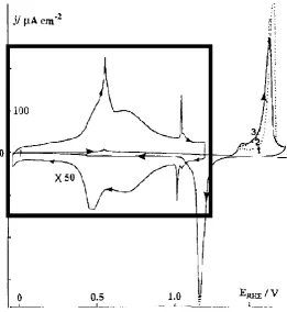
H2SO4 electrolyte contains a defined pattern, known as the “butterfly” peak in the
[image:38.595.188.450.172.457.2]double layer region. This occurs due to sulfate adsorption on the electrode surface, and the quality of this butterfly peak can be used to check the quality of a Au(111) surface.
Figure 14: Cyclic voltammograms of a Au(111) surface in a H2SO4 electrolyte. The
butterfly peak is contained in the black box and has been enlarged. This occurs due to the adsorption of sulfate anions. Figure adapted from reference 69.
21
1.3 The History Of STM
The scanning tunnelling microscope (STM) was invented in 1981 by Gerd Binnig, Heinrich Rohrer and colleagues of the IBM Zurich Research Laboratory.74-78 To this day, STM remains one of the most important surface characterisation techniques and can be used to image and manipulate individual atoms on a substrate surface in several different environments, including under UHV, ambient conditions (in air), under a liquid medium and also at extreme temperatures. Two years after its invention, atomic resolution was achieved using STM.77 Since then, atomic resolution of a great number of conducting substrates has been achieved, including for example Au(111), both bare and with an organothiol monolayer, Highly Ordered Pyrolytic Graphite (HOPG), and iodine adsorption on Pt(111), to name a few examples.79-81
A schematic diagram of an STM set up is shown in Figure 15. The tip is first moved under visual observation as close to the substrate as possible. A stepper motor then approaches the tip to the substrate up to a specified current. The precision control which allows the STM to work over such small areas is attained by the use of piezo crystals, which expand/contract when a voltage is applied. The piezo crystals then move the tip to the tunnelling current specified. This is known as the setpoint current (Iset). A bias voltage between the tip and sample must be applied to obtain a
tunnelling current (VBIAS).
Figure 15:Schematic of a Scanning Tunnelling Microscope. The STM tip is a fine needle which is scanned across a substrate surface. A bias voltage is applied between
22
contained in the scanner expand and contract with application of voltage and these are used to provide the fine precision control of the tip.
There are two methods of imaging a surface. The first is constant current mode. A feedback loop maintains the current and the output is a plot of the height of the tip. The second method for STM imaging is constant height mode. The feedback loop maintains the height and the output is a plot of current. This method is only suitable for very flat surfaces otherwise the tip would be susceptible to crashing.
1.3.1 Quantum Tunnelling
Figure 16:Quantum tunnelling through a potential barrier. In the tip and surface, the energy of the electron (E) is greater than the potential (V). However, in the gap between the electrodes, the potential is larger than the energy of the electron so the
electron is forbidden to be located in this region according to classical mechanics. However, quantum mechanics allows the electron to “tunnel” through the gap, as the
probability of the electronic wavefunction being present across the gap is > 0.
23
[ ]
Equation 1.2
When the electron resides in the region where E > V, which describes the metallic contacts, then the solution to the Schrödinger equation is:
Equation 1.3
Where A and B are constants, describes the wavefunction, i is an imaginary number which explains the oscillation of , and k is the wave vector:
√ ( ) Equation 1.4
In the classically forbidden region where E < V, the current has an exponential decay, hence the Schrödinger equation has a solution of the form:
Equation 1.5
Where κ is a decay constant. The further into the barrier, the lower the probability of the electron being present, hence the decay.
√ ( ) Equation 1.6
In the case of STM, the tip and substrate are the regions where E>V and the electronic wavefunction oscillates. The barrier, where the electron is classically forbidden to exist and where V>E is the gap between the tip and substrate. Provided this barrier is thin enough, then electrons will tunnel between the STM tip and substrate and a current will flow.
It has been shown that at low temperature and voltage, the tunnelling current is proportional to the distance of the tip from the surface.85
Equation 1.7
24
√ Equation 1.8
Where ϕ is the workfunction.
This means that the further away the tip is from the surface, the lower the tunnelling current will be. The exponential dependence on tip-sample separation is shown in Figure 17, from exponential data recorded during retraction of an STM tip.
Figure 17: Current-distance plot demonstrating the current exponential decay as the STM tip is withdrawn from the substrate surface. This plot was taken in a BMIOTf medium, the STM tip was Au wire and the substrate was a gold-on-glass substrate.
The decay constant for this plot is -11.69 nm-1.
1.4 STM In Single Molecule Electronics 1.4.1 Electron Transport
The previous section describes the simplest model of vacuum tunnelling between two metals along a one dimensional barrier. Electron transport across a molecule positioned between two metallic contacts is rarely adequately described by such a simple model. Much depends on the type of molecular wire used. The length of the molecule23, 86, 87, the terminating group88, 89 and redox properties30, 32, 33, 40-43, 45-47,
25
1.4.2 Coherent Transport
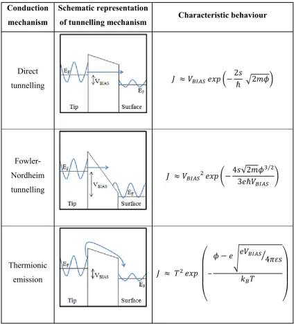
[image:43.595.106.534.234.703.2]Coherent transport occurs when the electron resides on the molecule for a short enough period of time that it does not inelastically interact with any particles within the molecule.
Table 2:Table of possible coherent electron transfer mechanisms (adapted from references 19, 82, and 104)
Conduction mechanism
Schematic representation
of tunnelling mechanism Characteristic behaviour
Direct
tunnelling (
√ )
Fowler-Nordheim tunnelling
( √
)
Thermionic
emission
(
√ ⁄
)
26
a barrier of reduced effective width, as illustrated in Table 2. In general, coherent transport is temperature independent, with the exception of thermionic emission, which has an exponential temperature dependence.105 Thermionic emission differs from both direct and Fowler-Nordheim tunnelling, as the electron is excited over the potential barrier as opposed to tunnelling through it. As can be predicted, thermionic emission depends strongly on the temperature of the system as well as the width of the potential barrier.19, 82, 88, 104
1.4.3 Superexchange
Superexchange is a coherent regime which occurs when the molecular orbitals aid ET despite being far away from the Fermi level of the metallic contacts. This is also described as “off-resonant” ET. Superexchange is particularly significant in the natural world as it is believed that electron transfer in photosynthesis occurs through this mechanism.106
Figure 18: Non-resonant coherent superexchange tunnelling through a molecular bridge. In the superexchange tunnelling mechanism, the electron transfer is aided by
the molecular orbital despite its large distance from the Fermi levels of the metallic contacts.
1.4.4 Simmons Model
27
and LUMO of the molecular bridge in question. When the electrons tunnel via a molecular orbital, then a different tunnelling regime dominates, which is explained later.
( )
{
( ) [ ( ) ( ) ]
( ) [ ( ) ( ) ] }
Equation 1.9
There is a typing error in reference 107 for equation (26). This mistake has been rectified in this thesis for Equation 1.9.
J is the tunnel current density, VBIAS is the bias voltage applied and β is a correction
factor which can be taken to be 1 when VBIAS < .107, 108 The addition of the
constant α is used for fitting. The exact physical meaning of α is unclear, although it has been suggested that it takes into account the effective mass of the tunnelling electron meff, or the barrier being non-rectangular.19, 23, 104, 108
With modification, the Simmons model can take into account the image charge, which in turn would affect the transmission probability by rounding the potential barrier and reducing the effective width. This is represented in Figure 19. The Simmons model only considers a rectangular barrier and not a rounded barrier, so is replaced with the effective rectangular barrier height:
(
)
Equation 1.10
Where c is approximately equal to 0.288/ϕεr, εr is the relative permittivity of the
barrier. Δs is the change in barrier width and is given by:23, 108
( )
⁄ Equation 1.11
28
Figure 19:Representation of the Simmons model, describing direct tunnelling. The original Simmons model rectangular barrier is shown in green. When image charge is
taken into account, the potential barrier is reduced in height and rounded (red). Since the Simmons model employs rectangular barriers, the effective height and width of
the potential barrier are used (blue). This representation is not to scale.
1.4.5 Double Barrier Tunnelling
The conductance of a molecular wire can be increased by sandwiching a barrier indentation between two tunnelling barriers.90, 110, 111 The presence of this barrier indentation facilitates electron transfer as it is easier for an electron to tunnel through two shorter barriers than one long barrier. This is demonstrated by a comparison of dodecanedithiol and the redox-active viologen moiety, which are both very similar in length. Electron transport through dodecanedithiol proceeds via direct tunnelling resulting in a conductance of (0.122 ± 0.014) nS,26 whereas Haiss et al. find that the presence of a barrier indentation endows the viologen with a significantly greater conductance of (0.44 ± 0.04) nS at 0 V vs SCE.40 Double barrier tunnelling is a well-known phenomenon in semiconductor devices and was first observed by Chang et al. in 1974.110 The semiconductor used was n-type GaAs, containing layers of Ga0.3Al0.7As layers, which act as tunnelling barriers. Semiconductor devices which
29
1.4.6 Resonant Tunnelling
Coherent resonant electron tunnelling is a two-step ET mechanism which involves the molecular orbitals of the molecular bridge. When the LUMO or HOMO lie close to the EF of the electrodes, then electron (hole) transport is dominated by the orbital
lying close to the Fermi level.19, 42, 95, 102, 112, 113 Resonant tunnelling is one of the dominant electron transfer regimes through a redox-active molecule.34, 95 The redox state of the molecular wire is altered by varying the sample potential. Around the redox potential of the molecule, there is a large increase in conductance, as more electrons can more favourably traverse the molecule at the redox potential.
Figure 20: Resonant tunnelling through a molecular bridge. The electron tunnels via a molecular orbital which results in an increase in conductance compared to direct
tunnelling where the molecular orbitals do not aid tunnelling to such an extent.
30
λsolv respectively, which are combined to give the total reorganisation energy λreorg, as
described by Schmickler and Tao.97, 113 Changes in λintra and λsolv may also change the
shape of the peak, resulting in the appearance of a shoulder. This can be compared to the Kuznetsov-Ulstrup model of ET, described below, where the λreorg affects the
[image:48.595.178.454.199.403.2]height of the current peak.
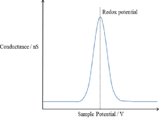
Figure 21:A plot of conductance vs. sample potential, showing the conductance increase at the redox potential of the molecular wire, a feature of resonant tunnelling.
1.4.7 Kuznetsov-Ulstrup Electron Transfer Model
Resonant tunnelling may also involve a vibrational relaxation of the orbital which aids the electron tunnelling.34, 42, 99, 114-116 The first step involves the electron tunnelling from the tip (assuming a positive sample bias) to the unoccupied molecular orbital. Due to solvent fluctuations, the LUMO may move closer to the Fermi level of the tip, which initiates the first ET.42 How the second step proceeds depends on the strength of the electronic coupling between the redox centre and the electrodes (tip and substrate). For strong electronic coupling, once the electron is present on the LUMO of the redox centre, this orbital then undergoes a partial vibrational relaxation, as the Kuznetsov-Ulstrup (KU) model suggests.41, 42, 93, 94, 99,
102, 114-116 In this scenario, the electron tunnels via the LUMO of the molecular wire.
31
vibrational relaxation is complete; before the LUMO relaxes below the Fermi level of the second electrode. This process may be repeated, as once the LUMO is vacated, it then relaxes towards higher energies, towards the Fermi level of the first electrode, resulting in a “boost” of the current. This is known as the adiabatic regime.42, 93, 102 The equation describing the adiabatic KU model of ET is shown below in Equation 1.12.31, 42, 116
( )
{ [ ( ) ]
[
( ) ]}
Equation 1.12
Where Ie is the enhanced current, κ is the electronic transmission coefficient, which is
assumed to be 1 in the adiabatic regime, ρ is the density of electronic states in the electrodes near the Fermi level, ω is the characteristic nuclear vibration frequency, VBIAS is the bias potential, λreorg is the reorganisation energy, η is the overpotential
applied to the substrate, and ξ and γ are modelling parameters relating to the proportion of electrochemical potential and the bias potential respectively, that affect the redox moiety.42 Equation 1.12 can be simplified when the same values of κ and ρ are assumed for both ET steps and using the approximation κρωe2/4π = 9.1x10⁻⁷ C2eV-1s-1.31, 42
{ [
( ) ]
[
( ) ]}
Equation 1.13
Assuming η and VBIAS are lower than λreorg, the above equation can be simplified to42:
[ ( [ ( ( ) )] )]
Equation 1.14
32
Figure 22: Adiabatic two-step electron transfer with partial vibrational relaxation. The electron tunnels to the LUMO, which then relaxes in energy after being reduced.
The electron vacates the LUMO it reaches the EF of the second electrode. The
re-oxidised LUMO can then relax back up to higher energies, where this process repeats itself. This results in a “boost” of current.
1.4.8 Marcus Theory
The Nobel Prize winning Marcus Theory of electron transfer explains the reorganisation energy λreorg, which is an important component of the above KU
model. Marcus Theory describes ET in a solution between two spherical species.84,
117-121 How fast the ET proceeds is dependent on the activation energy ΔG‡.
( )
Equation 1.15
The Marcus Theory can be described using potential energy diagrams, where the energy is plotted against the reaction coordinate, as shown in Figure 23. (A) is known as the “normal” region and ΔG‡ = 0.25(λreorg). As E, the difference in energy
between the two redox states gets larger, the reaction rate increases. (B) is the “activationless” region and ΔG‡ = 0. In this region, the ET proceeds very quickly and λreorg = E. As E gets larger, one enters the “inverted” region, where the reaction rate
33
Figure 23: Energy curves depicting the Marcus Theory of ET. (A) shows the ET in the “normal” region, (B) is “activationless” and (C) is the “inverted” region.121
The Marcus Theory explains that the reorganisation energy λreorg consists of two
components added together, the “inner-sphere” λintra which is the reorganisation
energy of intramolecular interactions as the ET occurs, such as orbitals, and the “outer-sphere” λsolv which describes how the solvent reorganises around the species
at the ET. λsolv can be calculated with relative ease in a solution.117, 118, 122
( ) ( ( ) ( ) ) ( ) Equation 1.16
ε0 is the relative permittivity of free space, RA and RB are the ionic radii, r is the
distance between the centre of the ions, which is taken to be RA + RB. n is the
refractive index of the solvent and εr is the relative permittivity of the solvent.118, 122
A simple example of the Marcus Theory in practice is a self-exchange reaction, a well-known example being:121
(Fe(OH2)6)3+ + (Fe(OH2)6)2+ → (Fe(OH2)6)2+ + (Fe(OH2)6)3+