Introduction to Microcontrollers
Courses 182.064 & 182.074
Vienna University of Technology Institute of Computer Engineering Embedded Computing Systems Group
February 26, 2007
Version 1.4
Contents
1 Microcontroller Basics 1
1.1 Introduction . . . 1
1.2 Frequently Used Terms . . . 6
1.3 Notation . . . 7
1.4 Exercises . . . 8
2 Microcontroller Components 11 2.1 Processor Core . . . 11
2.1.1 Architecture. . . 11
2.1.2 Instruction Set . . . 15
2.1.3 Exercises . . . 21
2.2 Memory . . . 22
2.2.1 Volatile Memory . . . 23
2.2.2 Non-volatile Memory. . . 27
2.2.3 Accessing Memory . . . 29
2.2.4 Exercises . . . 31
2.3 Digital I/O . . . 33
2.3.1 Digital Input . . . 34
2.3.2 Digital Output . . . 38
2.3.3 Exercises . . . 39
2.4 Analog I/O . . . 40
2.4.1 Digital/Analog Conversion . . . 40
2.4.2 Analog Comparator. . . 41
2.4.3 Analog/Digital Conversion . . . 42
2.4.4 Exercises . . . 51
2.5 Interrupts . . . 52
2.5.1 Interrupt Control . . . 52
2.5.2 Interrupt Handling . . . 55
2.5.3 Interrupt Service Routine . . . 57
2.5.4 Exercises . . . 59
2.6 Timer . . . 60
2.6.1 Counter . . . 60
2.6.2 Input Capture . . . 62
2.6.3 Output Compare . . . 65
2.6.4 Pulse Width Modulation . . . 65
2.6.5 Exercises . . . 66
2.7 Other Features. . . 68
2.7.1 Watchdog Timer . . . 68
2.7.2 Power Consumption and Sleep . . . 69
2.7.3 Reset . . . 70
2.7.4 Exercises . . . 71
3 Communication Interfaces 73 3.1 SCI (UART) . . . 75
3.2 SPI. . . 82
3.3 IIC (I2C) . . . 83
3.3.1 Data Transmission . . . 84
3.3.2 Speed Control Through Slave . . . 87
3.3.3 Multi-Master Mode . . . 87
3.3.4 Extended Addresses . . . 88
3.4 Exercises . . . 88
4 Software Development 89 4.1 Development Cycle . . . 91
4.1.1 Design Phase . . . 91
4.1.2 Implementation . . . 92
4.1.3 Testing & Debugging . . . 94
4.2 Programming . . . 97
4.2.1 Assembly Language Programming . . . 97
4.3 Download . . . 117
4.3.1 Programming Interfaces . . . 117
4.3.2 Bootloader . . . 118
4.3.3 File Formats . . . 118
4.4 Debugging. . . 121
4.4.1 No Debugger . . . 121
4.4.2 ROM Monitor . . . 124
4.4.3 Instruction Set Simulator . . . 124
4.4.4 In-Circuit Emulator . . . 125
4.4.5 Debugging Interfaces . . . 125
4.5 Exercises . . . 127
5 Hardware 129 5.1 Switch/Button . . . 129
5.2 Matrix Keypad . . . 130
5.3 Potentiometer . . . 132
5.4 Phototransistor . . . 132
5.5 Position Encoder . . . 133
5.6 LED . . . 134
5.7 Numeric Display . . . 135
5.8 Multiplexed Display . . . 136
5.9 Switching Loads . . . 138
5.10 Motors. . . 140
5.10.1 Basic Principles of Operation . . . 140
5.10.2 DC Motor . . . 142
5.10.3 Stepper Motor . . . 146
5.11 Exercises . . . 153
Index 159
Preface
This text has been developed for the introductory courses on microcontrollers taught by the Institute of Computer Engineering at the Vienna University of Technology. It introduces undergraduate stu-dents to the field of microcontrollers – what they are, how they work, how they interface with their I/O components, and what considerations the programmer has to observe in hardware-based and em-bedded programming. This text is not intended to teach one particular controller architecture in depth, but should rather give an impression of the many possible architectures and solutions one can come across in today’s microcontrollers. We concentrate, however, on small 8-bit controllers and their most basic features, since they already offer enough variety to achieve our goals.
Since one of our courses is a lab and uses the ATmega16, we tend to use this Atmel microcontroller in our examples. But we also use other controllers for demonstrations if appropriate.
For a few technical terms, we also give their German translations to allow our mainly German-speaking students to learn both the English and the German term.
Please help us further improve this text by notifying us of errors. If you have any sugges-tions/wishes like better and/or more thorough explanations, proposals for additional topics, . . . , feel free to email us at [email protected].
Chapter 1
Microcontroller Basics
1.1
Introduction
Even at a time when Intel presented the first microprocessor with the 4004 there was alrady a demand for microcontrollers: The contemporary TMS1802 from Texas Instruments, designed for usage in cal-culators, was by the end of 1971 advertised for applications in cash registers, watches and measuring instruments. The TMS 1000, which was introduced in 1974, already included RAM, ROM, and I/O on-chip and can be seen as one of the first microcontrollers, even though it was called a microcom-puter. The first controllers to gain really widespread use were the Intel 8048, which was integrated into PC keyboards, and its successor, the Intel 8051, as well as the 68HCxx series of microcontrollers from Motorola.
Today, microcontroller production counts are in the billions per year, and the controllers are inte-grated into many appliances we have grown used to, like
• household appliances (microwave, washing machine, coffee machine, . . . )
• telecommunication (mobile phones)
• automotive industry (fuel injection, ABS, . . . ) • aerospace industry
• industrial automation
• . . .
But what is this microcontroller we are talking about? What is the difference to a microprocessor? And why do we need microcontrollers in the first place? To answer these questions, let us consider a simple toy project: A heat control system. Assume that we want to
• periodically read the temperature (analog value, is digitized by sensor; uses 4-bit interface),
• control heating according to the temperature (turn heater on/off; 1 bit),
• display the current temperature on a simple 3-digit numeric display (8+3 bits),
• allow the user to adjust temperature thresholds (buttons; 4 bits), and
• be able to configure/upgrade the system over a serial interface.
So we design aprinted-circuit board(PCB) using Zilog’s Z80 processor. On the board, we put a Z80 CPU, 2 PIOs (parallel I/O; each chip has 16 I/O lines, we need 20), 1 SIO (serial I/O; for commu-nication to the PC), 1 CTC (Timer; for periodical actions), SRAM (for variables), Flash (for program
memory), and EEPROM (for constants).1 The resulting board layout is depicted in Figure1.1; as you can see, there are a lot of chips on the board, which take up most of the space (euro format, 10×16 cm).
Figure 1.1: Z80 board layout for 32 I/O pins and Flash, EEPROM, SRAM.
Incidentally, we could also solve the problem with the ATmega16 board we use in the Microcon-troller lab. In Figure 1.2, you can see the corresponding part of this board superposed on the Z80 PCB. The reduction in size is about a factor 5-6, and the ATmega16 board has even more features than the Z80 board (for example an analog converter)! The reason why we do not need much space for the ATmega16 board is that all those chips on the Z80 board are integrated into the ATmega16 microcontroller, resulting in a significant reduction in PCB size.
This example clearly demonstrates the difference between microcontroller and microprocessor: A microcontroller is a processor with memory and a whole lot of other components integrated on one chip. The example also illustrates why microcontrollers are useful: The reduction of PCB size saves time, space, and money.
The difference between controllers and processors is also obvious from their pinouts. Figure1.3
shows the pinout of the Z80 processor. You see a typical processor pinout, with address pins A0 -A15, data pins D0-D7, and some control pins like INT, NMI or HALT. In contrast, the ATmega16 has neither address nor data pins. Instead, it has 32 general purpose I/O pins PA0-PA7, PB0-PB7,
1.1. INTRODUCTION 3
Figure 1.2: ATmega16 board superposed on the Z80 board.
Figure 1.3: Pinouts of the Z80 processor (left) and the ATmega16 controller (right).
PC0-PC7, PD0-PD7, which can be used for different functions. For example, PD0 and PD1 can be used as the receive and transmit lines of the built-in serial interface. Apart from the power supply, the only dedicated pins on the ATmega16 are RESET, external crystal/oscillator XTAL1 and XTAL2, and analog voltage reference AREF.
Now that we have convinced you that microcontrollers are great, there is the question of which microcontroller to use for a given application. Since costs are important, it is only logical to select the cheapest device that matches the application’s needs. As a result, microcontrollers are generally tailored for specific applications, and there is a wide variety of microcontrollers to choose from.
archi-tecture. All controllers of a family contain the same processor core and hence are code-compatible, but they differ in the additional components like the number of timers or the amount of memory. There are numerous microcontrollers on the market today, as you can easily confirm by visiting the webpages of one or two electronics vendors and browsing through their microcontroller stocks. You will find that there are many different controller families like 8051, PIC, HC, ARM to name just a few, and that even within a single controller family you may again have a choice of many different controllers.
Controller Flash SRAM EEPROM I/O-Pins A/D Interfaces
(KB) (Byte) (Byte) (Channels)
AT90C8534 8 288 512 7 8
AT90LS2323 2 128 128 3
AT90LS2343 2 160 128 5
AT90LS8535 8 512 512 32 8 UART, SPI
AT90S1200 1 64 15
AT90S2313 2 160 128 15
ATmega128 128 4096 4096 53 8 JTAG, SPI, IIC
ATmega162 16 1024 512 35 JTAG, SPI
ATmega169 16 1024 512 53 8 JTAG, SPI, IIC
ATmega16 16 1024 512 32 8 JTAG, SPI, IIC
ATtiny11 1 64 5+1 In
ATtiny12 1 64 6 SPI
ATtiny15L 1 64 6 4 SPI
ATtiny26 2 128 128 16 SPI
[image:10.595.81.516.201.456.2]ATtiny28L 2 128 11+8 In
Table 1.1: Comparison of AVR 8-bit controllers (AVR, ATmega, ATtiny).
Table1.12shows a selection of microcontrollers of Atmel’s AVR family. The one thing all these
controllers have in common is their AVR processor core, which contains 32general purposeregisters and executes most instructions within one clock cycle.
After the controller family has been selected, the next step is to choose the right controller for the job (see [Ber02] for a more in-depth discussion on selecting a controller). As you can see in Table1.1(which only contains the most basic features of the controllers, namely memory, digital and analog I/O, and interfaces), the controllers vastly differ in their memory configurations and I/O. The chosen controller should of course cover the hardware requirements of the application, but it is also important to estimate the application’s speed and memory requirements and to select a controller that offers enough performance. For memory, there is a rule of thumb that states that an application should take up no more than 80% of the controller’s memory – this gives you some buffer for later additions. The rule can probably be extended to all controller resources in general; it always pays to have some reserves in case of unforseen problems or additional features.
Of course, for complex applications a before-hand estimation is not easy. Furthermore, in 32-bit microcontrollers you generally also include an operating system to support the application and
1.1. INTRODUCTION 5
its development, which increases the performance demands even more. For small 8-bit controllers, however, only the application has to be considered. Here, rough estimations can be made for example based on previous and/or similar projects.
The basic internal designs of microcontrollers are pretty similar. Figure 1.4 shows the block diagram of a typical microcontroller. All components are connected via an internal bus and are all integrated on one chip. The modules are connected to the outside world via I/O pins.
ControllerInterrupt EEPROM/
Flash Core
Processor
Serial Interface
Module
Analog Module
Counter/ Timer Module Microcontroller
... ...
Internal Bus SRAM
Module Digital I/O
Figure 1.4: Basic layout of a microcontroller.
The following list contains the modules typically found in a microcontroller. You can find a more detailed description of these components in later sections.
Processor Core: The CPU of the controller. It contains the arithmetic logic unit, the control unit, and the registers (stack pointer, program counter, accumulator register, register file, . . . ).
Memory: The memory is sometimes split into program memory and data memory. In larger con-trollers, a DMA controller handles data transfers between peripheral components and the mem-ory.
Interrupt Controller: Interrupts are useful for interrupting the normal program flow in case of (im-portant) external or internal events. In conjunction with sleep modes, they help to conserve power.
Timer/Counter: Most controllers have at least one and more likely 2-3 Timer/Counters, which can be used to timestamp events, measure intervals, or count events.
Many controllers also contain PWM (pulse width modulation) outputs, which can be used to drive motors or for safe breaking (antilock brake system, ABS). Furthermore the PWM output can, in conjunction with an external filter, be used to realize a cheap digital/analog converter.
Analog I/O: Apart from a few small controllers, most microcontrollers have integrated analog/digital converters, which differ in the number of channels (2-16) and their resolution (8-12 bits). The analog module also generally features an analog comparator. In some cases, the microcontroller includes digital/analog converters.
Interfaces: Controllers generally have at least one serial interface which can be used to download the program and for communication with the development PC in general. Since serial interfaces can also be used to communicate with external peripheral devices, most controllers offer several and varied interfaces like SPI and SCI.
Many microcontrollers also contain integrated bus controllers for the most common (field)busses. IIC and CAN controllers lead the field here. Larger microcontrollers may also contain PCI, USB, or Ethernet interfaces.
Watchdog Timer: Since safety-critical systems form a major application area of microcontrollers, it is important to guard against errors in the program and/or the hardware. The watchdog timer is used to reset the controller in case of software “crashes”.
Debugging Unit: Some controllers are equipped with additional hardware to allow remote debug-ging of the chip from the PC. So there is no need to download special debugdebug-ging software, which has the distinct advantage that erroneous application code cannot overwrite the debug-ger.
Contrary to processors, (smaller) controllers do not contain a MMU (Memory Management Unit), have no or a very simplified instruction pipeline, and have no cache memory, since both costs and the ability to calculate execution times (some of the embedded systems employing controllers are real-time systems, like X-by-wire systems in automotive control) are important issues in the micro-controller market.
To summarize, a microcontroller is a (stripped-down) processor which is equipped with memory, timers, (parallel) I/O pins and other on-chip peripherals. The driving element behind all this is cost: Integrating all elements on one chip saves space and leads to both lower manufacturing costs and shorter development times. This saves both time and money, which are key factors in embedded systems. Additional advantages of the integration are easy upgradability, lower power consumption, and higher reliability, which are also very important aspects in embedded systems. On the downside, using a microcontroller to solve a task in software that could also be solved with a hardware solution will not give you the same speed that the hardware solution could achieve. Hence, applications which require very short reaction times might still call for a hardware solution. Most applications, however, and in particular those that require some sort of human interaction (microwave, mobile phone), do not need such fast reaction times, so for these applications microcontrollers are a good choice.
1.2
Frequently Used Terms
Before we concentrate on microcontrollers, let us first list a few terms you will frequently encounter in the embedded systems field.
1.3. NOTATION 7
operated stand-alone, at the very least it requires some memory and an output device to be useful.
Please note that a processor is no controller. Nevertheless, some manufacturers and vendors list their controllers under the term “microprocessor”. In this text we use the termprocessor just for the processor core (the CPU) of a microcontroller.
Microcontroller: A microcontroller already contains all components which allow it to operate stand-alone, and it has been designed in particular for monitoring and/or control tasks. In conse-quence, in addition to the processor it includes memory, various interface controllers, one or more timers, an interrupt controller, and last but definitely not least general purpose I/O pins which allow it to directly interface to its environment. Microcontrollers also include bit opera-tions which allow you to change one bit within a byte without touching the other bits.
Mixed-Signal Controller: This is a microcontroller which can process both digital and analog sig-nals.
Embedded System: A major application area for microcontrollers are embedded systems. In em-bedded systems, the control unit is integrated into the system3. As an example, think of a cell
phone, where the controller is included in the device. This is easily recognizable as an embed-ded system. On the other hand, if you use a normal PC in a factory to control an assembly line, this also meets many of the definitions of an embedded system. The same PC, however, equipped with a normal operating system and used by the night guard to kill time is certainly no embedded system.
Real-Time System: Controllers are frequently used in real-time systems, where the reaction to an event has to occur within a specified time. This is true for many applications in aerospace, railroad, or automotive areas, e.g., for brake-by-wire in cars.
Embedded Processor: This term often occurs in association with embedded systems, and the differ-ences to controllers are often very blurred. In general, the term “embedded processor” is used for high-end devices (32 bits), whereas “controller” is traditionally used for low-end devices (4, 8, 16 bits). Motorola for example files its 32 bit controllers under the term “32-bit embedded processors”.
Digital Signal Processor (DSP): Signal processors are used for applications that need to —no sur-prise here— process signals. An important area of use are telecommunications, so your mobile phone will probably contain a DSP. Such processors are designed for fast addition and multi-plication, which are the key operations for signal processing. Since tasks which call for a signal processor may also include control functions, many vendors offer hybrid solutions which com-bine a controller with a DSP on one chip, like Motorola’s DSP56800.
1.3
Notation
There are some notational conventions we will follow throughout the text. Most notations will be explained anyway when they are first used, but here is a short overview:
3The exact definition of what constitutes an embedded system is a matter of some dispute. Here is an example definition of an online-encyclopaedia [Wik]:
An embedded system is a special-purpose computer system built into a larger device. An embedded system is typically required to meet very different requirements than a general-purpose personal computer.
• When we talk about the values of digital lines, we generally mean their logical values, 0 or 1. We indicate the complement of a logical valueX withX, so1 = 0and0 = 1.
• Hexadecimal values are denoted by a preceding $or 0x. Binary values are either given like decimal values if it is obvious that the value is binary, or they are marked with(·)2.
• The notation M[X] is used to indicate a memory access at address X.
• In our assembler examples, we tend to use general-purpose registers, which are labeled with R and a number, e.g., R0.
• The∝sign means “proportional to”.
• In a few cases, we will need intervals. We use the standard interval notations, which are [.,.] for a closed interval, [.,.) and (.,.] for half-open intervals, and (.,.) for an open interval. Variables denoting intervals will be overlined, e.g.dlatch = (0,1]. The notationdlatch+2adds the constant to the interval, resulting in(0,1] + 2 = (2,3].
• We use k as a generic variable, so do not be surprised ifk means different things in different sections or even in different paragraphs within a section.
Furthermore, you should be familiar with the followingpower prefixes4:
Name Prefix Power Name Prefix Power
kilo k 103 milli m 10−3
mega M 106 micro µ, u 10−6
giga G 109 nano n 10−9
tera T 1012 pico p 10−12
peta P 1015 femto f 10−15
exa E 1018 atto a 10−18
zetta Z 1021 zepto z 10−21
yotta Y 1024 yocto y 10−24
Table 1.2: Power Prefixes
1.4
Exercises
Exercise 1.1What is the difference between a microcontroller and a microprocessor?
Exercise 1.2Why do microcontrollers exist at all? Why not just use a normal processor and add all necessary peripherals externally?
Exercise 1.3 What do you believe are the three biggest fields of application for microcontrollers? Discuss you answers with other students.
Exercise 1.4Visit the homepage of some electronics vendors and compare their stock of microcon-trollers.
(a) Do all vendors offer the same controller families and manufacturers?
1.4. EXERCISES 9
(b) Are prices for a particular controller the same? If no, are the price differences significant?
(c) Which controller families do you see most often?
Exercise 1.5Name the basic components of a microcontroller. For each component, give an example where it would be useful.
Exercise 1.6What is anembedded system? What is areal-time system? Are these terms synonyms? Is one a subset of the other? Why or why not?
Exercise 1.7Why are there so many microcontrollers? Wouldn’t it be easier for both manufacturers and consumers to have just a few types?
Chapter 2
Microcontroller Components
2.1
Processor Core
The processor core (CPU) is the main part of any microcontroller. It is often taken from an existing processor, e.g. the MC68306 microcontroller from Motorola contains a 68000 CPU. You should al-ready be familiar with the material in this section from other courses, so we will briefly repeat the most important things but will not go into details. An informative book about computer architecture is [HP90] or one of its successors.
2.1.1
Architecture
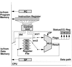
Control Unit
SP Memory
Program to/from
Memory to/from Data
File Register
Result OP src1
src2 dst
R0 R1 R2 R3
ALU Instruction Register
PC
Flags
Z N O C Status(CC) Reg
CPU
[image:17.595.152.443.412.679.2]Data path
Figure 2.1: Basic CPU architecture.
A basic CPU architecture is depicted in Figure 2.1. It consists of the data path, which executes instructions, and of thecontrol unit, which basically tells the data path what to do.
Arithmetic Logic Unit
At the core of the CPU is thearithmetic logic unit (ALU), which is used to perform computations (AND, ADD, INC, . . . ). Several control lines select which operation the ALU should perform on the input data. The ALU takes two inputs and returns the result of the operation as its output. Source and destination are taken from registers or from memory. In addition, the ALU stores some information about the nature of the result in thestatus register(also calledcondition code register):
Z (Zero): The result of the operation is zero.
N (Negative): The result of the operation is negative, that is, the most significant bit (msb) of the result is set (1).
O (Overflow): The operation produced an overflow, that is, there was a change of sign in a two’s-complement operation.
C (Carry): The operation produced a carry.
Two’s complement
Since computers only use 0 and 1 to represent numbers, the question arose how to represent negative integer numbers. The basic idea here is to invert all bits of a positive integer to get the corresponding negative integer (this would be theone’s complement). But this method has the slight drawback that zero is represented twice (all bits 0 and all bits 1). Therefore, a better way is to represent negative numbers by inverting the positive number and adding 1. For +1 and a 4-bit representation, this leads to:
1 = 0001→ −1 = 1110 + 1 = 1111.
For zero, we obtain
0 = 0000→ −0 = 1111 + 1 = 0000,
so there is only one representation for zero now. This method of representation is called the
two’s complement and is used in microcontrollers. With n bits it represents values within
[−2n−1,2n−1−1].
Register File
The register file contains the working registers of the CPU. It may either consist of a set ofgeneral purpose registers(generally 16–32, but there can also be more), each of which can be the source or destination of an operation, or it consists of some dedicated registers. Dedicated registers are e.g. anaccumulator, which is used for arithmetic/logic operations, or anindex register, which is used for some addressing modes.
2.1. PROCESSOR CORE 13
Example: Use of Status Register
The status register is very useful for a number of things, e.g., for adding or subtracting numbers that exceed the CPU word length. The CPU offers operations which make use of the carry flag, like ADDCa(add with carry). Consider for example the operation 0x01f0 + 0x0220 on an 8-bit CPUb c:
CLC ; clear carry flag
LD R0, #0xf0 ; load first low byte into register R0
ADDC R0, #0x20 ; add 2nd low byte with carry (carry <- 1)
LD R1, #0x01 ; load first high byte into R0
ADDC R1, #0x02 ; add 2nd high byte, carry from
; previous ADC is added
The first ADDC stores 0x10 into R0, but sets the carry bit to indicate that there was an overflow. The second ADDC simply adds the carry to the result. Since there is no overflow in this second operation, the carry is cleared. R1 and R0 contain the 16 bit result 0x0410. The same code, but with a normal ADD (which does not use the carry flag), would have resulted in 0x0310.
aWe will sometimes use assembler code to illustrate points. We do not use any specific assembly language or
instruction set here, but strive for easily understood pseudo-code.
bA # before a number denotes a constant.
cWe will denote hexadecimal values with a leading$(as is generally done in Assembly language) or a leading 0x(as is done in C).
Stack Pointer
Thestack is a portion of consecutive memory in the data space which is used by the CPU to store return addresses and possibly register contents during subroutine and interrupt service routine calls. It is accessed with the commands PUSH (put something on the stack) and POP (remove something from the stack). To store the current fill level of the stack, the CPU contains a special register called thestack pointer (SP), which points to the top of the stack. Stacks typically grow “down”, that is, from the higher memory addresses to the lower addresses. So the SP generally starts at the end of the data memory and is decremented with every push and incremented with every pop. The reason for placing the stack pointer at the end of the data memory is that your variables are generally at the start of the data memory, so by putting the stack at the end of the memory it takes longest for the two to collide.
Unfortunately, there are two ways to interpret the memory location to which the SP points: It can either be seen as the first free address, so a PUSH should store data there and then decrement the stack pointer as depicted in Figure2.21(the Atmel AVR controllers use the SP that way), or it can be seen as the last used address, so a PUSH first decrements the SP and then stores the data at the new address (this interpretation is adopted for example in Motorola’s HCS12). Since the SP must be initialized by the programmer, you must look up how your controller handles the stack and either initialize the SP
SP
SP
$FF $FF0x01
0x02
0x01 0x02
$FF0x01 SP $FF0x01
SP
$FF 0x02
0x01 0x02
R0
$FF0x01 0x02
SP SP
[image:20.595.205.384.85.290.2]Pop R2 Push 0x02 Push 0x01
Figure 2.2: Stack operation (write first).
to the last address in memory (if a push stores first and decrements afterwards) or to the last address + 1 (if the push decrements first).
As we have mentioned, the controller uses the stack during subroutine calls and interrupts, that is, whenever the normal program flow is interrupted and should resume later on. Since the return address is a pre-requisite for resuming program execution after the point of interruption, every controller pushes at least the return address onto the stack. Some controllers even save register contents on the stack to ensure that they do not get overwritten by the interrupting code. This is mainly done by controllers which only have a small set of dedicated registers.
Control Unit
Apart from some special situations like a HALT instruction or the reset, the CPU constantly executes program instructions. It is the task of thecontrol unitto determine which operation should be executed next and to configure the data path accordingly. To do so, another special register, the program counter (PC), is used to store the address of the next program instruction. The control unit loads this instruction into the instruction register (IR), decodes the instruction, and sets up the data path to execute it. Data path configuration includes providing the appropriate inputs for the ALU (from registers or memory), selecting the right ALU operation, and making sure that the result is written to the correct destination (register or memory). The PC is either incremented to point to the next instruction in the sequence, or is loaded with a new address in the case of a jump or subroutine call. After a reset, the PC is typically initialized to $0000.
2.1. PROCESSOR CORE 15
easy to add new and complex instructions, and instruction sets grew rather large and powerful as a result. This earned the architecture the nameComplex Instruction Set Computer (CISC). Of course, the powerful instruction set has its price, and this price is speed: Microcoded instructions execute slower than hard-wired ones. Furthermore, studies revealed that only 20% of the instructions of a CISC machine are responsible for 80% of the code (80/20 rule). This and the fact that these com-plex instructions can be implemented by a combination of simple ones gave rise to a movement back towards simple hard-wired architectures, which were correspondingly calledReduced Instruction Set Computer(RISC).
RISC: The RISC architecture has simple, hard-wired instructions which often take only one or a few clock cycles to execute. RISC machines feature a small and fixed code size with comparatively few instructions and few addressing modes. As a result, execution of instructions is very fast, but the instruction set is rather simple.
CISC: The CISC architecture is characterized by its complex microcoded instructions which take many clock cycles to execute. The architecture often has a large and variable code size and offers many powerful instructions and addressing modes. In comparison to RISC, CISC takes longer to execute its instructions, but the instruction set is more powerful.
Of course, when you have two architectures, the question arises which one is better. In the case of RISC vs. CISC, the answer depends on what you need. If your solution frequently employs a powerful instruction or addressing mode of a given CISC architecture, you probably will be better off using CISC. If you mainly need simple instructions and addressing modes, you are most likely better off using RISC. Of course, this choice also depends on other factors like the clocking frequencies of the processors in question. In any case, you must know what you require from the architecture to make the right choice.
Von Neumann versus Harvard Architecture
In Figure 2.1, instruction memory and data memory are depicted as two separate entities. This is not always the case, both instructions and data may well be in one shared memory. In fact, whether program and data memory are integrated or separate is the distinction between two basic types of architecture:
Von Neumann Architecture: In this architecture, program and data are stored together and are ac-cessed through the same bus. Unfortunately, this implies that program and data accesses may conflict (resulting in the famousvon Neumann bottleneck), leading to unwelcome delays.
Harvard Architecture: This architecture demands that program and data are in separate memories which are accessed via separate buses. In consequence, code accesses do not conflict with data accesses which improves system performance. As a slight drawback, this architecture requires more hardware, since it needs two busses and either two memory chips or a dual-ported memory (a memory chip which allows two independent accesses at the same time).
2.1.2
Instruction Set
Example: CISC vs. RISC
Let us compare a complex CISC addressing mode with its implementation in a RISC architec-ture. The 68030 CPU from Motorola offers the addressing mode “memory indirect preindexed, scaled”:
MOVE D1, ([24,A0,4*D0])
This operation stores the contents of register D1 into the memory address
24 + [A0] + 4∗[D0]
where square brackets designate “contents of” the register or memory address.
To simulate this addressing mode on an Atmel-like RISC CPU, we need something like the following:
LD R1, X ; load data indirect (from [X] into R1)
LSL R1 ; shift left -> multiply with 2
LSL R1 ; 4*[D0] completed
MOV X, R0 ; set pointer (load A0)
LD R0, X ; load indirect ([A0] completed)
ADD R0, R1 ; add obtained pointers ([A0]+4*[D0])
LDI R1, $24 ; load constant ($ = hex)
ADD R0, R1 ; and add (24+[A0]+4*[D0])
MOV X, R0 ; set up pointer for store operation
ST X, R2 ; write value ([24+[A0]+4*[D0]] <- R2)
In this code, we assume that R0 takes the place of A0, X replaces D0, and R2 contains the value of D1.
Although the RISC architecture requires 10 instructions to do what the 68030 does in one, it is actually not slower: The 68030 instruction takes 14 cycles to complete, the corresponding RISC code requires 13 cycles, assuming that all instructions take one clock cycle, except memory load/store, which take two.
• Instruction Size • Execution Speed
• Available Instructions • Addressing Modes
Instruction Size
An instruction contains in its opcode information about both the operation that should be executed and its operands. Obviously, a machine with many different instructions and addressing modes requires longer opcodes than a machine with only a few instructions and addressing modes, so CISC machines tend to have longer opcodes than RISC machines.
2.1. PROCESSOR CORE 17
Example: Some opcodes of the ATmega16
The ATmega16 is an 8-bit harvard RISC controller with a fixed opcode size of 16 or in some cases 32 bits. The controller has 32 general purpose registers. Here are some of its instructions with their corresponding opcodes.
instruction result operand conditions opcode
ADD Rd, Rr Rd + Rd←Rr 0≤d≤31, 0000 11rd dddd rrrr
0≤r ≤31
AND Rd, Rr Rd←Rd & Rr 0≤d≤31, 0010 00rd dddd rrrr
0≤r ≤31
NOP 0000 0000 0000 0000
LDI Rd, K Rd←K 16≤d≤31, 1110 KKKK dddd KKKK
0≤K ≤255
LDS Rd, k Rd←[k] 0≤d≤31, 1001 000d dddd 0000
0≤k ≤65535 kkkk kkkk kkkk kkkk
Note that the LDI instruction, which loads a register with a constant, only operates on the upper 16 out of the whole 32 registers. This is necessary because there is no room in the 16 bit to store the 5th bit required to address the lower 16 registers as well, and extending the operation to 32 bits just to accommodate one more bit would be an exorbitant waste of resources.
The last instruction, LDS, which loads data from the data memory, actually requires 32 bits to accommodate the memory address, so the controller has to perform two program memory accesses to load the whole instruction.
what you need. For instance, the 10 lines of ATmega16 RISC code require 20 byte of code (each instruction is encoded in 16 bits), whereas the 68030 instruction fits into 4 bytes. So here, the 68030 clearly wins. If, however, you only need instructions already provided by an architecture with short opcodes, it will most likely beat a machine with longer opcodes. We say “most likely” here, because CISC machines with long opcodes tend to make up for this deficit withvariable size instructions. The idea here is that although a complex operation with many operands may require 32 bits to encode, a simple NOP (no operation) without any arguments could fit into 8 bits. As long as the first byte of an instructions makes it clear whether further bytes should be decoded or not, there is no reason not to allow simple instructions to take up only one byte. Of course, this technique makes instruction fetching and decoding more complicated, but it still beats the overhead of a large fixed-size opcode. RISC machines, on the other hand, tend to feature short but fixed-size opcodes to simplify instruction decoding.
Obviously, a lot of space in the opcode is taken up by the operands. So one way of reducing the instruction size is to cut back on the number of operands that are explicitly encoded in the opcode. In consequence, we can distinguish four different architectures, depending on how many explicit operands a binary operation like ADD requires:
Stack Architecture: This architecture, also called0-address format architecture, does not have any explicit operands. Instead, the operands are organized as a stack: An instruction like ADD takes the top-most two values from the stack, adds them, and puts the result on the stack.
ac-cumulator which is always used as one of the operands and as the destination register. The second operand is specified explicitly.
2-address Format Architecture: Here, both operands are specified, but one of them is also used as the destination to store the result. Which register is used for this purpose depends on the processor in question, for example, the ATmega16 controller uses the first register as implicit destination, whereas the 68000 processor uses the second register.
3-address Format Architecture: In this architecture, both source operands and the destination are explicitly specified. This architecture is the most flexible, but of course it also has the longest instruction size.
Table2.1shows the differences between the architectures when computing (A+B)*C. We assume that in the cases of the 2- and 3-address format, the result is stored in the first register. We also assume that the 2- and 3-address format architectures areload/store architectures, where arithmetic instructions only operate on registers. The last line in the table indicates where the result is stored.
stack accumulator 2-address format 3-address format
PUSH A LOAD A LOAD R1, A LOAD R1, A
PUSH B ADD B LOAD R2, B LOAD R2, B
ADD MUL C ADD R1, R2 ADD R1, R1, R2
PUSH C LOAD R2, C LOAD R2, C
MUL MUL R1, R2 MUL R1, R1, R2
stack accumulator R1 R1
Table 2.1: Comparison between architectures.
Execution Speed
The execution speed of an instruction depends on several factors. It is mostly influenced by the complexity of the architecture, so you can generally expect a CISC machine to require more cycles to execute an instruction than a RISC machine. It also depends on the word size of the machine, since a machine that can fetch a 32 bit instruction in one go is faster than an 8-bit machine that takes 4 cycles to fetch such a long instruction. Finally, the oscillator frequency defines the absolute speed of the execution, since a CPU that can be operated at 20 MHz can afford to take twice as many cycles and will still be faster than a CPU with a maximum operating frequency of 8 MHz.
Available Instructions
Of course, the nature of available instructions is an important criterion for selecting a controller. Instructions are typically parted into several classes:
2.1. PROCESSOR CORE 19
Shift operations, which move the contents of a register one bit to the left or to the right, are typically provided both as logical and as arithmetical operations. The difference lies in their treatment of the most significant bit when shifting to the right (which corresponds to a division by 2). Seen arithmetically, the msb is the sign bit and should be kept when shifting to the right. So if the msb is set, then an arithmetic right-shift will keep the msb set. Seen logically, however, the msb is like any other bit, so here a right-shift will clear the msb. Note that there is no need to keep the msb when shifting to the left (which corresponds to a multiplication by 2). Here, a simple logical shift will keep the msb set anyway as long as there is no overflow. If an overflow occurs, then by not keeping the msb we simply allow the result to wrap, and the status register will indicate that the result has overflowed. Hence, an arithmetic shift to the left is the same as a logical shift.
Example: Arithmetic shift
To illustrate what happens in an arithmetic shift to the left, consider a 4-bit machine. Negative numbers are represented in two’s complement, so for example -7 is represented as binary 1001. If we simply shift to the left, we obtain 0010 = 2, which is the same as -14 modulo 16. If we had kept the msb, the result would have been 1010 = -6, which is simply wrong.
Shifting to the right can be interpreted as a division by two. If we arithmetically right-shift -4 = 1100, we obtain 1110 = -2 since the msb remains set. In a logical shift to the right, the result would have been 0110 = 6.
Data Transfer: These operations transfer data between two registers, between registers and memory, or between memory locations. They contain the normal memory access instructions like LD (load) and ST (store), but also the stack access operations PUSH and POP.
Program Flow: Here you will find all instructions which influence the program flow. These include jump instructions which set the program counter to a new address, conditional branches like BNE (branch if the result of the prior instruction was not zero), subroutine calls, and calls that return from subroutines like RET or RETI (return from interrupt service routine).
Control Instructions: This class contains all instructions which influence the operation of the con-troller. The simplest such instruction is NOP, which tells the CPU to do nothing. All other special instructions, like power-management, reset, debug mode control, . . . also fall into this class.
Addressing Modes
When using an arithmetic instruction, the application programmer must be able to specify the in-struction’s explicit operands. Operands may be constants, the contents of registers, or the contents of memory locations. Hence, the processor has to provide means to specify the type of the operand. While every processor allows you to specify the above-mentioned types, access to memory locations can be done in many different ways depending on what is required. So the number and types of addressing modes provided is another important characteristic of any processor. There are numerous addressing modes2, but we will restrict ourselves to the most common ones.
immediate/literal: Here, the operand is a constant. From the application programmer’s point of view, processors may either provide a distinct instruction for constants (like the LDI —load immediate— instruction of the ATmega16), or require the programmer to flag constants in the assembler code with some prefix like #.
register: Here, the operand is the register that contains the value or that should be used to store the result.
direct/absolute: The operand is a memory location.
register indirect: Here, a register is specified, but it only contains the memory address of the actual source or destination. The actual access is to this memory location.
autoincrement: This is a variant of indirect addressing where the contents of the specified register is incremented either before (pre-increment) or after (post-increment) the access to the memory location. The post-increment variant is very useful for iterating through an array, since you can store the base address of the array as an index into the array and then simply access each element in one instruction, while the index gets incremented automatically.
autodecrement: This is the counter-part to the autoincrement mode, the register value gets decre-mented either before or after the access to the memory location. Again nice to have when iterating through arrays.
displacement/based: In this mode, the programmer specifies a constant and a register. The contents of the register is added to the constant to get the final memory location. This can again be used for arrays if the constant is interpreted as the base address and the register as the index within the array.
indexed: Here, two registers are specified, and their contents are added to form the memory address. The mode is similar to the displacement mode and can again be used for arrays by storing the base address in one register and the index in the other. Some controllers use a special register as the index register. In this case, it does not have to be specified explicitly.
memory indirect: The programmer again specifies a register, but the corresponding memory loca-tion is interpreted as a pointer, i.e., it contains the final memory localoca-tion. This mode is quite useful, for example for jump tables.
Table 2.2shows the addressing modes in action. In the table, M[x]is an access to the memory address x, d is the data size, and #n indicates a constant. The notation is taken from [HP90] and varies from controller to controller.
As we have already mentioned, CISC processors feature more addressing modes than RISC pro-cessors, so RISC processors must construct more complex addressing modes with several instructions. Hence, if you often need a complex addressing mode, a CISC machine providing this mode may be the wiser choice.
Before we close this section, we would like to introduce you to a few terms you will often en-counter:
• An instruction set is called orthogonalif you can use every instruction with every addressing mode.
• If it is only possible to address memory with special memory access instructions (LOAD, STORE), and all other instructions like arithmetic instructions only operate on registers, the architecture is called aload/store architecture.
2.1. PROCESSOR CORE 21
addressing mode example result
immediate ADD R1, #5 R1←R1 + 5
register ADD R1, R2 R1←R1 + R2
direct ADD R1, 100 R1←R1 + M[100]
register indirect ADD R1, (R2) R1←R1 + M[R2]
post-increment ADD R1, (R2)+ R1←R1 + M[R2]
R2←R2 +d
pre-decrement ADD R1,−(R2) R2←R2−d
R1←R1 + M[R2]
displacement ADD R1, 100(R2) R1←R1 + M[100 + R2]
indexed ADD R1, (R2+R3) R1←R1 + M[R2+R3]
memory indirect ADD R1, @(R2) R1←R1 + M[M[R2]]
Table 2.2: Comparison of addressing modes.
2.1.3
Exercises
Exercise 2.1.1What are the advantages of the Harvard architecture in relation to the von Neumann architecture? If you equip a von Neumann machine with a dual-ported RAM (that is a RAM which allows two concurrent accesses), does this make it a Harvard machine, or is there still something missing?
Exercise 2.1.2Why was RISC developed? Why can it be faster to do something with several instruc-tions instead of just one?
Exercise 2.1.3What are the advantages of general-purpose registers as opposed to dedicated regis-ters? What are their disadvantages?
Exercise 2.1.4In Section2.1.2, we compared different address formats. In our example, the accumu-lator architecture requires the least instructions to execute the task. Does this mean that accumuaccumu-lator architectures are particularly code-efficient?
Exercise 2.1.5What are the advantages and drawbacks of a load/store architecture?
Exercise 2.1.6Assume that you want to access an array consisting of 10 words (a word has 16 bit) starting at memory address 100. Write an assembler program that iterates through the array (pseudo-code). Compare the addressing modes register indirect, displacement, auto-increment, and indexed.
2.2
Memory
In the previous chapter, you already encountered various memory types: Theregister fileis, of course, just a small memory embedded in the CPU. Also, we briefly mentioned data being transferred between registers and thedata memory, and instructions being fetched from theinstruction memory.
Therefore, an obvious distinction of memory types can be made according to their function:
Register File: A (usually) relatively small memory embedded on the CPU. It is used as a scratchpad for temporary storage of values the CPU is working with - you could call it the CPU’s short term memory.
Data Memory: For longer term storage, generic CPUs usually employ an external memory which is much larger than the register file. Data that is stored there may be short-lived, but may also be valid for as long as the CPU is running. Of course, attaching external memory to a CPU requires some hardware effort and thus incurs some cost. For that reason, microcontrollers usually sport on-chip data memory.
Instruction Memory: Like the data memory, the instruction memory is usually a relatively large external memory (at least with general CPUs). Actually, with von-Neumann-architectures, it may even be the same physical memory as the data memory. With microcontrollers, the instruction memory, too, is usually integrated right into the MCU.
These are the most prominent uses of memory in or around a CPU. However, there is more mem-ory in a CPU than is immediately obvious. Depending on the type of CPU, there can be pipeline registers, caches, various buffers, and so on.
About memory embedded in an MCU: Naturally, the size of such on-chip memory is limited. Even worse, it is often not possible to expand the memory externally (in order to keep the design simple). However, since MCUs most often are used for relatively simple tasks and hence do not need excessive amounts of memory, it is prudent to include a small amount of data and instruction memory on the chip. That way, total system cost is decreased considerably, and even if the memory is not expandable, you are not necessarily stuck with it: Different members in a MCU family usually provide different amounts of memory, so you can choose a particular MCU which offers the appropriate memory space.
Now, the functional distinction of memory types made above is based on the way the memory is used. From a programmer’s perspective, that makes sense. However, hardware or chip designers usu-ally view memory rather differently: They prefer to distinguish according to the physical properties of the electronic parts the memory is made of. There, the most basic distinction would be volatile
versusnon-volatilememory. In this context, volatile means that the contents of the memory are lost as soon as the system’s power is switched off.
Of course, there are different ways either type of memory can be implemented. Therefore, the distinction based on the physical properties can go into more detail. Volatile memory can bestaticor
dynamic, and there is quite a variety of non-volatile memory types: ROM,PROM,EPROM,EEPROM,
2.2. MEMORY 23
NVRAM
ROM PROM EPROM EEPROM EEPROMFlash
SRAM DRAM
Semiconductor Memory
volatile non−volatile
Figure 2.3: Types of Semiconductor Memory.
2.2.1
Volatile Memory
As mentioned above, volatile memory retains its contents only so long as the system is powered on. Then why should you use volatile memory at all, when non-volatile memory is readily available?
The problem here is that non-volatile memory is usually a lot slower, more involved to work with, and much more expensive. While the volatile memory in your PC has access times in the nanosecond range, some types of non-volatile memory will be unavailable for milliseconds after writing one lousy byte to them.
Where does the name RAM come from?
For historic reasons, volatile memory is generally calledRAM– Random Access Memory. Of course, the random part does not mean that chance is involved in accessing the memory. That acronym was coined at an early stage in the development of computers. Back then, there were different types of volatile memory: One which allowed direct access to any address, and one which could only be read and written sequentially (so-called shift register memory). Engineers decided to call the former type ‘random access memory’, to reflect the fact that, from the memory’s perspective, any ‘random’, i.e., arbitrary, address could be accessed. The latter type of memory is not commonly used any more, but the term RAM remains.
Static RAM
Disregarding the era of computers before the use of integrated circuits,Static Random Access Memory (SRAM)was the first type of volatile memory to be widely used. An SRAM chip consists of an array of cells, each capable of storing one bit of information. To store a bit of information, a so-called flip-flop is used, which basically consists of six transistors. For now, the internal structure of such a cell is beyond the scope of our course, so let’s just view the cell as a black box. Looking at Figure2.4, you see that one SRAM cell has the following inputs and outputs:
Data InDin On this input, the cell accepts the one bit of data to be stored.
Read/WriteR/W Via the logical value at this input, the type of access is specified: 0 means the cell is to be written to, i.e., the current state ofDinshould be stored in the cell. 1 means that the cell is to be read, so it should setDoutto the stored value.
Cell SelectCS As long as this input is logical 0, the cell does not accept any data present atDin and keeps its outputDout in a so-called high resistance state, which effectively disconnects it from the rest of the system. On a rising edge, the cell either accepts the state atDinas the new bit to store, or it setsDoutto the currently stored value.
Cell MemorySRAM
in
D R/W
[image:30.595.244.358.212.268.2]CS Dout
Figure 2.4: An SRAM cell as a black box.
To get a useful memory, many such cells are arranged in a matrix as depicted in Figure2.5. As you can see, allDout lines are tied together. If all cells would drive their outputs despite not being addressed, a short between GND and VCC might occur, which would most likely destroy the chip. Therefore, theCSline is used to select one cell in the matrix and to put all other cells into their high resistance state. To address one cell and hence access one particular bit, SRAMs need some extra logic to facilitate such addressing (note that we use, of course, a simplified diagram).
Din & Dout CS R/W Cell SRAM Din & Dout CS R/W Cell SRAM Din & Dout CS R/W Cell SRAM Din & Dout CS R/W Cell SRAM Din & Dout CS R/W Cell SRAM Din & Dout CS R/W Cell SRAM Din & Dout CS R/W Cell SRAM Din & Dout CS R/W Cell SRAM Din & Dout CS R/W Cell SRAM Din & Dout CS R/W Cell SRAM Din & Dout CS R/W Cell SRAM Din & Dout CS R/W Cell SRAM Din & Dout CS R/W Cell SRAM Din & Dout CS R/W Cell SRAM Din & Dout CS R/W Cell SRAM Din & Dout CS R/W Cell SRAM Din & Dout CS R/W Cell SRAM Din & Dout CS R/W Cell SRAM Din & Dout CS R/W Cell SRAM Din & Dout CS R/W Cell SRAM row0 row1 row2 row3
col0 col1 col2 col3
[image:30.595.104.492.437.720.2]2.2. MEMORY 25
As you can see in Figure2.5, a particular memory cell is addressed (i.e., its CS pulled high) when both its associated row and column are pulled high (the little squares with the ampersand in them are and-gates, whose output is high exactly when both inputs are high). The purpose is, of course, to save address lines. If we were to address each cell with an individual line, a 16Kx1 RAM (16 K bits), for example, would already require 16384 lines. Using the matrix layout with one and-gate per cell, 256 lines are sufficient.
While 256 address lines is much better than 16384, it is still inacceptably high for a device as simple as a 16Kx1 RAM – such pin counts would make your common microcontroller pale in com-parison. However, we can decrease the address line count further: No more than one row and one column can be selected at any given time – else we would address more than one memory cell at the same time. We can use this fact to reduce the number of necessary lines by adding so-called decoders. Ann-bit decoder is a component with n input pins and 2n output pins, which are numbered O0 to
O2n−1. At the input pins, a binary number bis presented, and the decoder setsOb to 1 and all other outputs to 0. So, instead of actually setting one of many rows, we just need the number of the row we wish to select, and the decoder produces the actual row lines. With that change, our 16Kx1 SRAM needs no more than 14 address lines.
Figure2.6depicts our SRAM from Figure2.5after adding the decoder.
Din & Dout CS R/W Cell SRAM Din & Dout CS R/W Cell SRAM Din & Dout CS R/W Cell SRAM Din & Dout CS R/W Cell SRAM Din & Dout CS R/W Cell SRAM Din & Dout CS R/W Cell SRAM Din & Dout CS R/W Cell SRAM Din & Dout CS R/W Cell SRAM Din & Dout CS R/W Cell SRAM Din & Dout CS R/W Cell SRAM Din & Dout CS R/W Cell SRAM Din & Dout CS R/W Cell SRAM Din & Dout CS R/W Cell SRAM Din & Dout CS R/W Cell SRAM Din & Dout CS R/W Cell SRAM Din & Dout CS R/W Cell SRAM Din & Dout CS R/W Cell SRAM Din & Dout CS R/W Cell SRAM Din & Dout CS R/W Cell SRAM Din & Dout CS R/W Cell SRAM row0 row1 row2 row3
col0 col1 col2 col3
A A A A 0 1 2 3
Figure 2.6: Further reducing the number of external address pins.
[image:31.595.82.517.347.688.2]So much for the internals of a SRAM. Now, what do we actually see from the outside? Well, a SRAM usually has the following external connections (most of which you already know from the layout of one memory cell):
Address LinesA0. . . An−1 We just talked about these. They are used to select one memory cell out of a total of2ncells.
Data In (Din) The function is basically the same as with one memory cell. For RAMs of width n≥2, this is actually a bus composed ofndata lines.
Data Out (Dout) Same function as in a single memory cell. Like Din, for RAMs of width n ≥ 2, this would be a bus.
Chip Select (CS) or Chip Enable (CE) This is what Cell Select was for the memory cell.
Read/Write (R/W) Again, this works just likeR/W in a memory cell.
Dynamic RAM
In contrast to a well known claim that nobody will ever need more than 640 kilobytes of RAM, there never seems to be enough memory available. Obviously, we would like to get as much storage capacity as possible out of a memory chip of a certain size.
Now, we already know that SRAM usually needs six transistors to store one single bit of infor-mation. Of course, the more transistors per cell are needed, the larger the silicon area will be. If we could reduce the number of components needed – say, we only use half as much transistors –, then we would get about twice the storage capacity.
That is what was achieved with Dynamic Random Access Memory – DRAM: The number of transistors needed per bit of information was brought down to one. This, of course, reduced the silicon area for a given cell count. So at the same chip size, a DRAM has much larger storage capacity compared to an SRAM.
How does that work? Well, instead of using a lot of transistors to build flip-flops, one bit of information is stored in acapacitor. Remember capacitors? They kind of work like little rechargeable batteries – you apply a voltage across them, and they store that voltage. Disconnect, and you have a loaded capacitor. Connect the pins of a loaded capacitor via a resistor, and an electrical current will flow, discharging the capacitor.
Now, where’s the one transistor per memory cell we talked about, since the information is stored in a capacitor? Well, the information is indeed stored in a capacitor, but in order to select it for reading or writing, a transistor is needed.
By now, it should be obvious how a DRAM works: If you want to store a logical one, you address the memory cell you want to access by driving the transistor. Then, you apply a voltage, which charges the capacitor. To store a logical zero, you select the cell and discharge the capacitor. Want to read your information back? Well, you just have to check whether the capacitor is charged or not. Simple.
2.2. MEMORY 27
So how did the engineers make DRAM work? Well, they kind of handed the problem over to the users: By accessing DRAM, the information is refreshed (the capacitors are recharged). So DRAM has to be accessed every few milliseconds or so, else the information is lost.
To remedy the refresh problem, DRAMs with built-in refresh logic are available, but that extra logic takes up a considerable portion of the chip, which is somewhat counter-productive and not necessarily needed: Often, the CPU does not need to access its RAM every cycle, but also has internal cycles to do its actual work. A DRAM refresh controller logic can use the cycles in between the CPUs accesses to do the refreshing.
DRAM has about four times larger storage capacity than SRAM at about the same cost and chip size. This means that DRAMs are available in larger capacities. However, that would also increase the number of address pins ⇒ larger package to accommodate them ⇒ higher cost. Therefore, it makes sense to reduce the number of external pins by multiplexing row and column number: First, the number of the row is presented at the address pins, which the DRAM internally stores. Then, the column number is presented. The DRAM combines it with the previously stored row number to form the complete address.
Apart from the need for memory refresh, there is another severe disadvantage of DRAM: It is much slower than SRAM. However, due to the high cost of SRAM, it is just not an option for common desktop PCs. Therefore, numerous variants of DRAM access techniques have been devised, steadily increasing the speed of DRAM memory.
In microcontrollers, you will usually find SRAM, as only moderate amounts of memory are needed, and the refresh logic required for DRAM would use up precious silicon area.
2.2.2
Non-volatile Memory
Contrary to SRAMs and DRAMs, non-volatile memories retain their content even when power is cut. But, as already mentioned, that advantage comes at a price: Writing non-volatile memory types is usually much slower and comparatively complicated, often downright annoying.
ROM
Read Only Memories (ROMs) were the first types of non-volatile semiconductor memories. Did we just say write access is more involved with non-volatile than with volatile memory? Well, in the case of ROM, we kind of lied: As the name implies, you simply cannot write to a ROM. If you want to use ROMs, you have to hand the data over to the chip manufacturer, where a specific chip is made containing your data.
A common type of ROM is the so-calledMask-ROM (MROM). An MROM, like any IC chip, is composed of several layers. The geometrical layout of those layers defines the chip’s function. Just like a RAM, an MROM contains a matrix of memory cells. However, during fabrication, on one layer fixed connections between rows and columns are created, reflecting the information to be stored in the MROM.
During fabrication of an IC, masks are used to create the layers. The name Mask-ROM is derived from the one mask which defines the row-column connections.
PROM
As an alternative, Programmable Read Only Memory(PROM) is available. These are basically matrices of memory cells, each containing a silicon fuse. Initially, each fuse is intact and each cell reads as a logical 1. By selecting a cell and applying a short but high current pulse, the cell’s fuse can be destroyed, thereby programming a logical 0 into the selected cell.
Sometimes, you will encounter so-calledOne Time Programmable(OTP) microcontrollers. Those contain PROM as instruction memory on chip.
PROMs and OTP microcontrollers are, of course, not suitable for development, where the content of the memory may still need to be changed. But once the development process is finished, they are well-suited for middle range mass production, as long as the numbers are low enough that production of MROMs is not economically feasible.
EPROM
Even after the initial development is finished and the products are already in use, changes are often necessary. However, with ROMs or OTP microcontrollers, to change the memory content the actual IC has to be replaced, as its memory content is unalterable.
Erasable Programmable Read Only Memory (EPROM) overcomes this drawback. Here, program-ming is non-destructive. Memory is stored in so-calledfield effect transistors(FETs), or rather in one of their pins called gate. It is aptly namedfloating gate, as it is completely insulated from the rest of the circuit. However, by applying an appropriately high voltage, it is possible to charge the floating gate via a physical process called avalanche injection. So, instead of burning fuses, electrons are injected into the floating gate, thus closing the transistor switch.
Once a cell is programmed, the electrons should remain in the floating gate indefinitely. However, as with DRAMs, minimal leakage currents flow through the non-perfect insulators. Over time, the floating gate loses enough electrons to become un-programmed. In the EPROM’s datasheet, the manufacturer specifies how long the memory content will remain intact; usually, this is a period of about ten years.
In the case of EPROMs, however, this limited durability is actually used to an advantage: By exposing the silicon chip to UV light, the process can be accelerated. After about 30 minutes, the UV light will have discharged the floating gates, and the EPROM is erased. That is why EPROMS have a little glass window in their package, through which the chip is visible. Usually, this window is covered by a light proof protective seal. To erase the EPROM, you remove the seal and expose the chip to intense UV light (since this light is strong enough to permanently damage the human eye, usually an EPROM eraser is used, where the EPROM is put into a light-proof box and then exposed to UV light).
Incidentally, often EPROMs are used as PROMs. So-called One Time Programmable EPROMs
(OTP-EPROMs) are common EPROMs, as far as the chip is concerned, but they lack the glass window in the package. Of course, they cannot be erased, but since the embedded glass window makes the package quite expensive, OTP-EPROMS are much cheaper to manufacture. The advantage over PROM is that when going to mass production, the type of memory components used does not change. After all, the OTP-EPROM used for mass production is, in fact, an EPROM just like the one used in prototyping and testing, just without the little window. To go from EPROM to PROM would imply a different component, with different electrical characteristics and possibly even different pinout.
EEPROM
2.2. MEMORY 29
erase them, a UV light source is needed. Obviously, a technological improvement was in order. The EEPROM (Electrically Erasable and Programmable ROM) has all the advantages of an EPROM without the hassle. No special voltage is required for programming anymore, and – as the name implies – no more UV light source is needed for erasing. EEPROM works very similar to EPROM, except that the electrons can be removed from the floating gate by applying an elevated voltage.
We got a little carried away there when we claimed that no special voltage is necessary: An elevated voltage is still needed, but it is provided on-chip via so-called charge pumps, which can generate higher voltages than are supplied to the chip externally.
Of course, EEPROMs have their limitations, too: They endure a limited number of write/erase-cycles only (usually in the order of 100.000 write/erase-cycles), and they do not retain their information indefi-nitely, either.
EEPROMs are used quite regularly in microcontroller applications. However, due to their limited write endurance, they should be used for longer term storage rather than as scratch memory. One example where EEPROMs are best used is the storage of calibration parameters.
Flash
Now, EEPROM seems to be the perfect choice for non-volatile memory. However, there is one drawback: It is rather expensive. As a compromise,FlashEEPROM is available. Flash is a variant of EEPROM where erasing is not possible for each address, but only for larger blocks or even the entire memory (erased ‘in aflash’, so to speak). That way, the internal logic is simplified, which in turn reduces the price considerably. Also, due to the fact that it is not possible to erase single bytes, Flash EEPROM is commonly used for program, not data memory. This, in turn, means that reduced endurance is acceptable – while you may reprogram a data EEPROM quite often, you will usually not reprogram a microcontroller’s program Flash 100.000 times. Therefore, Flash-EEPROMs often have a lower guaranteed write/erase cycle endurance compared to EEPROMs – about 1.000 to 10.000 cycles. This, too, makes Flash-EEPROMs cheaper.
NVRAM
Finally, there is a type of memory that combines the advantages of volatile and non-volatile memories:
Non-Volatile RAM (NVRAM). This can be achieved in different ways. One is to just add a small internal battery to an SRAM device, so that when external power is switched off, the SRAM still retains its content. Another variant is to combine a SRAM with an EEPROM in one package. Upon power-up, data is copied from the EEPROM to the SRAM. During operation, data is read from and written to the SRAM. When power is cut off, the data is copied to the EEPROM.
2.2.3
Accessing Memory
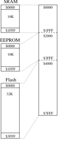
Many microcontrollers come with on-chip program and data memory. Usually, the program memory will be of the Flash-EEPROM type, and the data memory will be composed of some SRAM and some EEPROM. How does a particular address translate in terms of the memory addressed? Basically, there are two methods:
Flash EEPROM SRAM
$0000 $0000 $0000
$1FFF $1FFF
$3FFF
16K 16K
[image:36.595.222.372.86.210.2]32K
Figure 2.7: Separate Memory Addressing.
The address ranges of the three different memory types can be the same. The programmer specifies which memory is to be accessed by using different access methods. E.g., to access EEPROM, a specific EEPROM-index register is used.
• All memory types share a common address range, see Figure2.8(e.g. HCS12).
$0000
SRAM
EEPROM
$0000
$0000
$0000
Flash
$1FFF $2000
$3FFF $4000 $1FFF
$1FFF
$7FFF
$3FFF 16K
16K
32K
Figure 2.8: Different memory types mapped into one address range.
[image:36.595.249.348.349.587.2]