Influence of stress on optical transitions in GaN nanorods containing a single
InGaN/GaN quantum disk
Y. D. Zhuang, J. Bruckbauer, P. A. Shields, P. R. Edwards, R. W. Martin, and D. W. E. Allsopp
Citation: Journal of Applied Physics 116, 174305 (2014); doi: 10.1063/1.4898685 View online: http://dx.doi.org/10.1063/1.4898685
View Table of Contents: http://scitation.aip.org/content/aip/journal/jap/116/17?ver=pdfcov Published by the AIP Publishing
Articles you may be interested in
Cross-sectional sizes and emission wavelengths of regularly patterned GaN and core-shell InGaN/GaN quantum-well nanorod arrays
J. Appl. Phys. 113, 054315 (2013); 10.1063/1.4790710
Fabrication and luminescent properties of core-shell InGaN/GaN multiple quantum wells on GaN nanopillars Appl. Phys. Lett. 100, 261103 (2012); 10.1063/1.4731629
Symmetrically tunable optical properties of InGaN/GaN multiple quantum disks by an external stress Appl. Phys. Lett. 100, 171916 (2012); 10.1063/1.4709397
InGaN/GaN nanorod array white light-emitting diode Appl. Phys. Lett. 97, 073101 (2010); 10.1063/1.3478515
Excitation current dependent cathodoluminescence study of InGaN/GaN quantum wells grown on m-plane and c-plane GaN substrates
Influence of stress on optical transitions in GaN nanorods containing
a single InGaN/GaN quantum disk
Y. D. Zhuang,1J. Bruckbauer,2P. A. Shields,1P. R. Edwards,2R. W. Martin,2 and D. W. E. Allsopp1,a)
1
Department of Electronic and Electrical Engineering, University of Bath, Bath BA2 7AY, United Kingdom
2
Department of Physics, SUPA, University of Strathclyde, Glasgow G4 0NG, United Kingdom
(Received 26 June 2014; accepted 8 October 2014; published online 3 November 2014)
Cathodoluminescence (CL) hyperspectral imaging has been performed on GaN nanorods containing a single InGaN quantum disk (SQD) with controlled variations in excitation conditions. Two different nanorod diameters (200 and 280 nm) have been considered. Systematic changes in the CL spectra from the SQD were observed as the accelerating voltage of the electron beam and its position of incidence are varied. It is shown that the dominant optical transition in the SQD varies across the nanorod as a result of interplay between the contributions of the deformation potential and the quantum-confined Stark effect to the transition energy as consequence of radial variation in the pseudomorphic strain.VC 2014 AIP Publishing LLC.
[http://dx.doi.org/10.1063/1.4898685]
I. INTRODUCTION
Group III–nitride nanorods have attracted wide interest as a vehicle for studying their fundamental material proper-ties1as well as for their potential application in high bright-ness light emitting diodes.2–10 Compared with other III-V semiconductors, the III–nitrides show strong polarization especially along the c-axis with the effect that strain can have a major influence on the optical properties in InxAlyGa1–x–yN based quantum wells (QWs).11 The forma-tion of a nanorod structure, either by bottom-up epitaxial growth2–5 or by dry etching a pre-existing epitaxial III–nitride layer,6–10has been proposed as a mean of alleviat-ing strain due to the free surface presented by the sidewalls enabling the lattice to relax.12–14
In the case of homogeneous nanorods formed by dry etching from c-plane homo-epitaxial GaN templates, the degree of strain relaxation in the overall structure will depend on the diameter and height of the nanorods, with complete strain relaxation occurring when their height exceeds their diameter irrespective of the type of substrate used.15When such etched nanorods contain an InGaN QW or a MQW oriented in the c-plane changes in the optical transition energy have been observed and are frequently ascribed to the impact of the strain relaxation in the nanorod on the piezoelectric contribution to the quantum-confined Stark effect (QCSE).9 However, several theoretical studies have revealed that the effect of the distribution of the pseu-domorphic strain and the concomitant polarization variation is more complex.13,16One theoretical study has predicted not only the widely observed line shifts associated with the QCSE, but also multiple transitions associated with electrons and holes being localized in different positions across the ra-dius of the nanorod.13 Recently, evidence has emerged to support these predictions,17 but a comprehensive
measurement-based study is still required to identify the combined influences of the effects of axial and radial strain on light emission from c-plane oriented QWs, notably contri-butions to transition energies from the bulk deformation of the InGaN layer(s) and the QCSE.
This paper reports a detailed study of optical transitions in isolated, nominally fully relaxed GaN nanorods containing a single pseudomorphic InGaN QW by cathodoluminescence (CL) hyperspectral imaging. The CL system used combines high spectral resolution with high spatial resolution, to pro-vide positional information about the location of the observed optical transitions on a scale much smaller than the diameter of the nanorods18,19 and is therefore able to track changes in the luminescence associated with both radial and axial strain variations in the nanorods. The paper is organ-ized as follows. SectionIIpresents an overview of the struc-ture of nanorods, the methods used in their fabrication and the CL hyperspectral imaging system. Section IIIpresents a detailed description and discussion of the results and the con-clusions of the work are given in Sec.IV.
II. SAMPLE FABRICATION
The nanorods used in this research were fabricated by post-growth processing of a GaN epitaxial structure contain-ing a scontain-inglec-plane oriented InGaN QW grown by metal or-ganic chemical vapor deposition. The epitaxial structure, starting from the sapphire substrate, comprised a 4lm n-type GaN:Si layer, followed by a 2 nm wide InGaN single QW (emission wavelength 440 nm) and capped by a 0.5lm p-type GaN:Mg layer.
The nanorods were formed using a combined nano-imprint lithography/lift-off technique20to define a hexagonal array (600 nm pitch) of relatively thick (100 nm), 300 nm diameter nickel nano-dots to act as a dry etch mask. Nanorods of height 1.5lm were then formed by induc-tively coupled plasma (ICP) etching in Cl2and Ar at a
tem-perature of 150C, a process that produces high aspect ratio
a)Author to whom correspondence should be addressed. Electronic mail:
nanorods with vertical sidewalls.20 The damaged layer on the nanorod sidewalls introduced by ICP etching was removed by etching in KOH at 40C to produce an ordered array of regular shaped nanorods containing a single disk-shaped QW lying in thec-plane that emits strong photolumi-nescence (PL) at room temperature. Arrays of nanorods of different diameters (range 120–280 nm) were fabricated by cleaving the sample after ICP etching and then adjusting the duration of the KOH etching step. Single nanorods were formed for CL hyperspectral imaging by carefully cleaving some of the nanorods at their base from the underlying GaN layer.
III. RESULTS AND DISCUSSION
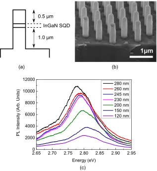
Fig.1(a)shows a schematic of the nanorod structure in which the 2 nm thick InGaN layer extends across the whole diameter to form in effect, a single quantum disk (SQD). Fig.1(b)shows a secondary electron (SE) image of an array of such nanorods and Fig.1(c) shows the variation with di-ameter of the PL room temperature PL emitted from each array of nanorods. The QW PL from the un-etched starting planar material is characterized by a single emission peak centered at 460 nm (not shown). On etching the nanorods, the SQD emission spectra of the various nanorods are pro-gressively blue shifted as the diameter is reduced from 280 nm to 200 nm with little further shift with further reduc-tion in diameter down to 120 nm. A second feature of the SQD is a broadening of the PL emission peak caused by the
emergence of a second transition close in energy, this occur-ring irrespective of the nanorod diameter. Similar broaden-ing associated with a second transition has been observed in low temperature micro PL performed on isolated nanorods fabricated in the same way from nominally the same planar epitaxial structure.21The lower energy of these two transi-tions was found to have a long decay constant, indicating that the recombining carriers were spatially separated within the SQD.21
CL hyperspectral imaging was performed in a field emission gun scanning electron microscope (FEI Sirion 200) modified for CL spectroscopy.18An advantage of the hyper-spectral imaging system used is its ability to measure shifts in emission wavelength on a length scale<20 nm,22thus en-abling precise mapping of CL spectral features. The CL was excited with an electron beam with accelerating voltage of 2 kV, 10 kV, or 30 kV, with the sample held at room temper-ature. Increasing the accelerating voltage increases the pene-tration depth of the electron beam and, for a fixed electron beam current, causes a much slower reduction in the spot size illuminated by the beam. Thus, the use of different accelerating voltages enables the impact of progressively increases in the penetration depth of the electron beam into the nanorod at different axial positions on the CL to be resolved. In this way, axial and radial variations in strain on the CL could be determined.
The magnitude of the beam current on the spatial resolu-tion achieved by varying the beam condiresolu-tions must be taken into account. For most measurements, the beam current was
FIG. 1. (a) Schematic of the nanorod structures containing a SQD; (b) SE image of an array of InGaN/GaN SQD nanorods with an average diameter of 280 nm, and (c) variation with nanorod diameter in the room temperature SQD PL (inset: nanorod diameters).
[image:3.612.51.368.423.768.2]held at 2 nA. Some measurements with a 10 kV beam were repeated for beam currents of 0.5 and 0. 1 nA to investigate the extent to which the excited charge carriers screen the polarization in the SQD. TableI shows the estimated elec-tron beam spot sizes under the different experimental condi-tions used.
Measurements were performed on both standing and felled nanorods, the latter formed by carefully cleaving the nanorods at their base from the underlying GaN layer. Two nanorod diameters were studied in detail: 280 nm and 200 nm, the latter being the minimum diameter for which variations in the SQD PL was observed. In the case of felled nanorods, the incident electron beam was scanned in a plane parallel to their long axis through the SQD starting and end-ing in the GaN layers above and below. For standend-ing nano-rods, the electron beam was incident at an angle of45 to
the nanorod sidewalls.
The CL spectrum at each point in the beam scan was dispersed by a spectrograph and recorded by an electron multiplying charge coupled device (EMCCD) to obtain multi-dimensional datasets combining both spectral and positional information.18 The measured spectra were smoothed using a high frequency filtering algorithm to remove noise introduced by the EMCCD.
Fig.2shows (a) the SE image of a single felled nanorod, and CL intensity maps of (b) the GaN band edge emission and (c) the SQD emission, all obtained at an accelerating voltage of 30 kV and beam current of 2 nA, which pro-duced a calculated beam spot size of4 nm. Scanning the nanorod with a beam of this size enables the CL emission spectra to be correlated to small volumes of the nanorod, en-abling CL images to be extracted by post-processing a single hyperspectral image dataset. The CL from the SQD is intense in comparison to the GaN band edge emission, with the latter only observed from below the SQD (right-hand side of the nanorod) owing to the p-type doping of the GaN layer above the InGaN SQD.
The peak energy of the GaN band edge CL was almost unchanged with the point of incidence of the electron beam position on the GaN layer below the InGaN SQD for all three accelerating voltages used; i.e., it was independent of beam penetration depth. This was the case for both standing and felled nanorods. Further, the peak energy of this GaN band edge CL correlated with that of unstrained material, from which it can be inferred that the GaN sections of the nano-rods wires were relaxed to a depth of>100 nm. The results conform with an earlier finding that virtually complete strain relaxation occurs in GaN nanorods with a height-to-diameter ratio>1 formed from continuous c-plane layers by essen-tially the same lithographic and dry etching process.23 Further, it can also be inferred that any strain in the InGaN
layer derives purely from lattice mismatch strain arising from pseudomorphic growth.
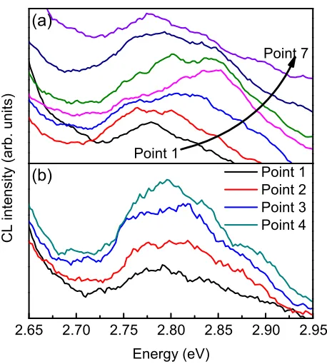
Fig.3(a)shows the spectral variation of the SQD emis-sion taken from selected line-scans in the hyperspectral image obtained from the same nanorod at the same accelerat-ing voltage and beam current at the positions indicated in Fig.2(a)by the line of white dots. Several felled nanorods of the same diameter were investigated in the same way and the following results are typical. As the beam traverses across the InGaN SQD, the CL emission band evolves from being dominated by a single peak at 2.78 eV at the sidewall of the nanorod (point 1) to being double peaked as a second peak at2.84 eV progressively emerges as the excited area moves toward the center of the rod (points 2, 3, and 4). At the center of the InGaN SQD, the peak at 2.84 eV domi-nates, and the evolution in the CL spectrum is reversed as the electron beam traverses to the other sidewall of the nano-rod (points 5, 6, and 7).
[image:4.612.323.554.65.357.2]Fig.3(b)shows the positional evolution, from edge-to-center, of the CL from the InGaN SQD excited by a 30 kV electron beam in a standing nanorod on the same sample. The pattern is similar to that for a felled nanorod with the higher energy peak emerging at the same position to within 1 meV when the electron beam is aligned to the center of the nanorod, although the intensity of the peak at 2.84 eV is less pronounced. The likely reason for this is the different
TABLE I. Estimated electron beam spot sizes.
Accelerating voltage 2 kV 10 kV 30 kV
Spot size for 2.1 nA beam current 10 nm 7 nm 4 nm Spot size for 0.5 nA beam current 3.5 nm
Spot size for 0.1 nA beam current 2 nm
[image:4.612.51.297.710.765.2]angles of incidence of the electron beam for the felled and standing nanorods. For standing nanorods, the electron beam is incident at an angle to the longitudinal axis of the nanorod, whereas for felled nanorod it is more aligned to the plane of the quantum well. The latter results in stronger excitation of the SQD, notably its inner core, evidenced by higher signal to noise ratio in Fig.3(a). Otherwise, the trends in the width and general shape of the spectra with position of entry of the electron beam from positions 1 through to 4 are the same for the felled and standing nanorods. Also, a second higher energy emission peak at 2.88 eV is also now resolved when the beam is aligned with the center of the SQD. The overall effect of the emergence and growth of the2.84 eV peak is to cause an apparent blue shift in the SQD emission peak and to increase its full width half maximum (FWHM) as the electron beam was scanned from edge to center of the InGaN disk. On continuing the scan to the opposite edge of the nanorod, the evolution of the line shape is reversed.
Changing the accelerating voltage caused systematic changes in the CL spectra. Fig.4shows the impact on the CL across the SQD in a felled nanorod after reducing the accelerating voltage to 10 kV. The beam current was again 2 nA, which for this beam voltage and current produced a beam spot size of7 nm diameter at the sample surface. The apparent blue shift in the SQD emission peak as the electron beam is scanned from edge to center is still observed at this lower beam voltage. (Points 1–7 correspond to those shown in Fig. 2(a)). However, the double-peak nature of the CL from the SQD is no longer clearly resolved and is evident only in a marked asymmetry in the emission band from the center of the nanorod (point 4). The symmetry in the edge-to-edge evolution of the SQD emission band with position of
the electron beam, notably the apparent shift in its peak energy, is now obvious.
Possible contributions to the spectral changes from the QCSE and from band filling were investigated by varying the beam current, and hence the densities of induced electron-hole pairs, at a constant accelerating voltage of 10 kV. The results from CL collected from the center of the InGaN SQD are shown in Fig.5. Increasing the beam current causes a red shift in the CL indicating that neither screening of the QCSE nor band filling plays a significant role in the observed spectral shifts with beam position as shown in Figs. 3and4, as both would be expected to cause a blue shift. A temperature rise caused by increasing beam current can also be discounted as the mean position of the CL emission spec-tra shown in Figures3and4is unchanged as the accelerating voltage, hence energy input to the nanorods, is increased by a factor three (from 10 to 30 kV). Rather, the changes in the CL spectra derive from position and accelerating voltage de-pendent excitation of two or more emission peaks within the SQD.
[image:5.612.59.288.58.313.2]FIG. 3. (a) InGaN SQD emission spectra as a function of lateral position in the InGaN SQD in a “felled” 280 nm diameter nanorod and (b) position de-pendent CL spectra of a “standing” nanorod of the same diameter. Both data sets were obtained at 30 kV and 2 nA beam current.
FIG. 4. Evolution with lateral position of the CL excited by an electron beam of accelerating voltage of 10 kV and 2 nA current from an identical felled GaN nanorod containing an InGaN SQD from the edge (points 1 and 7) to the center (point 4).
FIG. 5. Normalized CL spectra from the center of the InGaN SQD excited for three different nominal beam currents with the accelerating voltage held constant at 10 kV.
[image:5.612.321.550.61.235.2] [image:5.612.321.551.554.730.2]It has been shown that a radial strain gradient exists across the InGaN layer from its center to edge with its outer shell largely relaxed.14,24As such and noting that increasing the accelerating voltage of the electron beam increases its penetration depth into the nanorods, the changes in the observed CL with electron beam position and accelerating voltage should reflect the strain variation across the SQD.
In order to determine more precisely the changes in ex-citation volume with electron beam parameters, Monte Carlo simulations of the electron trajectories within a GaN layer were performed for accelerating voltages of 2, 10, and 30 kV using CASINO.25The resulting calculations of effective ex-citation volume for different electron beam alignments can then be correlated with the changes in the CL spectra. Fig.6 shows plots of the electron deposition profiles calculated from these trajectories for beam voltages of 2, 10, and 30 kV. Cross-sections of a 280 nm diameter nanorod with an assumed 20 nm wide shell in which strain is reduced have been superimposed on these electron profiles in positions corresponding to points 1 (edge) and 4 (center) in Figs.3and 4, to show how varying the alignment of the electron beam and its accelerating voltage enables building an excitation map of the SQD.
For example, Fig.6(a)shows that CL excited by a 2 kV beam derives only from a25 nm wide outer shell of the
SQD irrespective of its alignment. At the other extreme, a 30 kV beam will penetrate 120 nm into the nanorod with the excitation volume slowly widening from <5 nm at the surface to 15 nm at penetration depth of 120 nm. When aligned to the edge of the nanorod, there is strong excitation of the outer shell and some excitation of the core owing to the lateral beam spreading. On the other hand, when cen-trally aligned a 30 kV beam will strongly excite a significant fraction of the SQD core, whilst still exciting part of the outer shell, with the effect that the CL spectrum will be more representative of the core. For the 10 kV beam, the shape of the CL spectra should lie between these two extremes with the outer shell making a more dominant contribution for all beam alignments than in the case of the 30 kV beam, but with emission from the core still contributing except when the electron beam is aligned to the edge (beam positions 1 and 7 in Fig.2(a)).
Fig.7shows a comparison of the normalized CL inten-sity from (a) the edge and (b) the center of the same nanorod excited by electron beams of 2 kV, 10 kV, and 30 kV. The emission peaks of the three spectra taken from the edge of the nanorod coincide closely in energy at2.78 eV, with the 10 kV and 30 kV spectra somewhat broadened compared with that excited by the 2 kV beam, indicating that some emission from the core does contribute to the spectra but not much in the case of the 10 kV beam. On the other hand, the CL spectra from the center of the InGaN SQD excited by the 10 kV and 30 kV beams are noticeably blue shifted with respect to the 2 kV beam spectrum, which is almost unchanged from that taken from the edge of the SQD.
[image:6.612.50.290.381.714.2]Taking these data together with the calculations of beam penetration in Fig.6, it is inferred that the spectrum excited by the 2 kV beam, with its emission peak at2.78 eV, origi-nates from the outer shell of the SQD. The width of this shell is estimated from the penetration depth of the 2 keV electron beam to be 25 nm, a value very similar to the calculated width (20 nm) of the strain-relaxed layer of a freestanding nanorod of height greater than its diameter;4,24from which it is concluded that the 2.78 eV transition originates from strain-free material.
FIG. 6. Energy deposition profiles from Monte Carlo electron trajectory sim-ulations for (a) and (b) 2 kV, (c) and (d) 10 kV, and (e) and (f) 30 kV beams impinging on a GaN sample overlaid with cross sections of SQDs of a felled 280 nm nanorod containing a 20 nm fully relaxed outer shell material and strained inner core material.
[image:6.612.319.551.550.730.2]Further, the spectra in Fig. 7 taken together with the energy deposition profiles in Figs. 6(d) and6(f) for the 10 and 30 keV electron beams show that broadening of the CL peak by10–15 meV to higher energy derives from excita-tion of transiexcita-tions in the nanorod core, notably that at
2.84 eV observed in the spectra in Fig. 3. The degree of
broadening and the resolution of the contributing emission peaks in the spectrum will depend on the relative excitation of the core and outer shell of the SQD by the electron beam. When aligned to the edge of the nanorod, the difference in penetration depth of the 10 and 30 keV beams has little effect on the degree of excitation of the core and the spectra in both cases are dominated by the emission at2.78 eV from the outer shell. However, when the beams are aligned with the center of the nanorod, the greater penetration depth of the 30 keV electrons will cause relatively more excitation in the core than a 10 kV electron beam. This has the effect that the CL spectrum will contain a significantly stronger contri-bution from the 2.84 eV transition, as observed. On the other hand, CL spectra excited by the 10 keV beam comprise both emission peaks with a comparatively small change in the relative intensity of the2.78 eV and2.84 eV peaks as the beam scans from the edge to the center of the InGaN SQD. As a consequence, the CL spectrum appears broadened with the2.84 eV peak unresolved, as seen in Fig.4.
Taken as a whole, the data conform to a model in which the observed systematic changes in the CL emitted from the SQD arise from interplay between the QCSE and the defor-mation potential contribution to the transition energy as the pseudomorphic strain varies from its center to its edge. The QCSE contributes a blue shift in the ground state intersub-band transition of the SQD moving from its core to its outer shell as the piezoelectric polarization decreases owing to the strain relaxation at the sidewall. Simultaneously, the defor-mation potential contribution to the InGaN/GaN band gaps decreases as pseudomorphic strain is released at the outer edge of the nanorod, giving rise to a more dominant red shift moving from center to edge.13 Based on the correlation between the results of Monte Carlo simulations and the hyperspectral CL data, the width of relaxed outer shell is
25 nm, consistent with earlier estimates.14,24
Finally, the impact of reducing the diameter of the nano-rods has been considered. Fig.8shows CL spectra measured at five points across a SQD in a 200 nm diameter nanorod, obtained with an electron beam current of 130 pA and 10 kV accelerating voltage. Only five measurement points were considered in the thinner nanorods: points 1 and 5 corre-spond to the two edges of the SQD, point 3 lies at its center, and point 2 (4) lies approximately mid-way between points 1 (5) and 3. Since the width of the relaxed outer shell will be independent of nanorod diameter,7 the impact of reducing the nanorod diameter will be to increase the contribution of the outer shell contributes to the volume excited by the elec-tron beam relative to that contributed by the strained inner core. Thus, the lower energy CL peak (2.78 eV) will be more dominant in the spectrum than the emission at 2.84 eV from the strained nano-disk core, as observed in Fig.8, to provide further evidence for the interplay between bulk deformation and the QCSE in determining the optical
transition energies in pseudomorphicc-plane oriented InGaN QWs in GaN nanorods. The net effect of this interplay is for the lower energy transition energy to occur in the relaxed outer shell of the SQD, with possible Fermi level pinning at the SQD surface making the transition spatially indirect.14,24
IV. SUMMARY
CL hyperspectral imaging and Monte Carlo simulations of the electron excitation volume have been performed on an InGaN SQD embedded in GaN nanorods formed by post-growth nanoimprint lithography and ICP etching. The meas-urements were performed for nanorods of 280 nm and 200 nm diameter and for different accelerating voltages and beam currents. In all cases, the CL spectra contained two peaks, which are shown to be associated with a radial varia-tion in the ground state QW transivaria-tion in such a way that two distinct optical transitions closely spaced in energy occur at different radial positions in the nano-disk. This behavior is explained by the opposing impacts of the QCSE and the de-formation potential contributions to the transition energy with the radial strain variation from the center to edge of the InGaN SQD.
ACKNOWLEDGMENTS
The Authors wish to thank Osram for kindly providing the single quantum well epitaxy and Chris Chan of the University of Oxford, England, for his help in performing the micro-photoluminescence measurements.
1
F. A. Ponce and D. P. Bour,Nature386, 351 (1997).
2H.-M. Kim, Y.-H. Cho, H. Lee, S. I. Kim, S. R. Ryu, D. Y. Kim, T. W.
Kang, and K. S. Chung,Nano Lett.4, 1059 (2004).
3
H.-W. Lin, Y.-J. Lu, H.-Y. Chen, H.-M. Lee, and S. Gwo,Appl. Phys. Lett.97, 073101 (2010).
4W. Guo, M. Zhang, A. Banerjee, and P. Bhattacharya,Nano Lett.10, 3355
(2010).
5
S. Li and A. Waag,J. Appl.Phys.111, 071101 (2012).
6
S. Keller, C. Schaake, N. A. Fichtenbaum, C. J. Neufeld, Y. Wu, K. McGroddy, A. David, S. P. DenBaars, C. Weisbuch, J. S. Speck, and U. K. Mishra,J. Appl. Phys.100, 054314 (2006).
FIG. 8. (a) CL spectra measured at five points across an InGaN SQD embed-ded in a 200 nm diameter felled nanorod. Points 1 and 5 correspond to the edge and point 3 to the center of the nanorod.
[image:7.612.321.550.61.235.2]7C. H. Chiu, T. C. Lu, H. W. Huang, C. F. Lai, C. C. Kao, J. T. Chu, C. C.
Yu, H. C. Kuo, S. C. Wang, C. F. Lin, and T. H. Hsueh,Nanotechnology
18, 445201 (2007).
8
Q. Li, K. R. Westlake, M. H. Crawford, S. R. Lee, D. D. Koleske, J. J. Figiel, K. C. Cross, S. Fathololoumi, Z. Mi, and G. T. Wang,Opt. Express
19, 25528 (2011).
9
J. Bai, Q. Wang, and T. Wang,J. Appl. Phys.111, 113103 (2012).
10
Y. D. Zhuang, C. J. Lewins, S. Lis, P. A. Shields, and D. W. E. Allsopp,
IEEE Photon. Technol. Lett.25, 1047 (2013).
11S. Nakamura, T. Mukai, and M. Senoh,Appl. Phys. Lett.
64, 1687 (1994).
12
Y. Kawakami, S. Suzuki, A. Kaneta, M. Funato, A. Kikuchi, and K. Kishino,Appl. Phys. Lett.89, 163124 (2006).
13C. B€ocklin, R. G. Veprek, S. Steiger, and B. Witzigmann,Phys. Rev. B
81, 155306 (2010).
14
M. J. Holmes, Y. S. Park, X. Wang, C. C. S. Chan, A. F. Jarjour, R. A. Taylor, J. H. Warner, J. Luo, H. A. R. El-Ella, and R. A. Oliver,J. Appl. Phys.109, 063515 (2011).
15
W. J. Tseng, M. Gonzalez, L. Dillemans, K. Cheng, S. J. Jiang, P. M. Vereecken, G. Borghs, and R. R. Lieten,Appl. Phys. Lett.101, 253102 (2012).
16C. Rivera, U. Jahn, T. Flissikowski, J. L. Pau, E. Mu~noz, and H. T. Grahn,
Phys. Rev. B75, 045316 (2007).
17Y. D. Zhuang, S. Lis, J. Bruckbauer, S. E. J. O’Kane, P. A. Shields, P. R.
Edwards, J. Sarma, R. W. Martin, and D. W. E. Allsopp, Jpn. J. Appl. Phys., Part 152, 08JE11 (2013).
18
P. R. Edwards, L. K. Jagadamma, J. Bruckbauer, C. Liu, P. Shields, D. Allsopp, T. Wang, and R. W. Martin, Microsc. Microanal. 18, 1212 (2012).
19
J. Bruckbauer, P. R. Edwards, J. Bai, T. Wang, and R. W. Martin,
Nanotechnology24, 365704 (2013).
20P. Shields, M. Hugues, J. Zu~niga-Perez, M. Cooke, M. Dineen, W. Wang,
F. Causa, and D. Allsopp,Phys. Status Solidi C9, 631 (2012).
21
C. C. S. Chan, B. P. L. Reid, R. A. Taylor, Y. D. Zhuang, P. A. Shields, D. W. E. Allsopp, and W. Jia,Appl. Phys. Lett.102, 111906 (2013).
22J. Bruckbauer, P. R. Edwards, T. Wang, and R. W. Martin,Appl. Phys.
Lett.98, 141908 (2011).
23
M. Hugues, P. A. Shields, F. Sacconi, M. Mexis, M. Auf der Maur, M. Cooke, M. Dineen, A. Di Carlo, D. W. E. Allsopp, and J. Zu~niga-Perez,
J. Appl. Phys.114, 084307 (2013).
24
Y. Kawakami, A. Kaneta, L. Su, Y. Zhu, K. Okamoto, M. Funato, A. Kikuchi, and K. Kishino,J. Appl. Phys.107, 023522 (2010).
25D. Drouin, A. R. Couture, D. Joly, X. Tastet, V. Aimez, and R. Gauvin,