Optical Properties of GaN Nanorods Containing a Single or Multiple InGaN Quantum Wells
Yi D. Zhuang1, Szymon Lis1, Jochen Bruckbauer2, Simon E. J. O’Kane1, Philip A. Shields1, Paul R. Edwards2, Jayanta Sarma1, Robert W. Martin2, and Duncan W. E. Allsopp1 1Department of Electronic and Electrical Engineering, University of Bath, Bath BA2 7AY, U.K.
2Department of Physics, SUPA, University of Strathclyde, Glasgow G4 0NG, U.K. E-mail: [email protected]
Received October 12, 2012; revised November 17, 2012; accepted November 20, 2012; published online May 20, 2013
Measurements of light emission from GaN nanorods of diameter between 80 and 350 nm, containing either a three-well multiple InGaN quantum well or a single quantum well, have been performed by photoluminescence (PL) and cathodoluminescence (CL) hyperspectral imaging. The PL underwent a Stark shift to the blue as the nanorod diameter was reduced, indicating substantial relaxation of the compressive strain in the quantum wells. The intensity of the nanorod emission per unit area can exceed that of the planar starting material. The CL measurements revealed that the wavelength of the quantum well emission varied with radial position in the nanorod. Simulations by a modal expansion method revealed that the light extraction efficiency varies with radial position and the variation is dependent on nanorod diameter. Finite difference time domain simulations showed that Bloch mode formation in the buffer layer below the nanorods impacts on the light extraction.
#2013 The Japan Society of Applied Physics
1. Introduction
InGaN/GaN nanorod light emitting diodes (LEDs) have recently attracted attention owing to the possibility that such nanostructures may accommodate strain to enhance the internal quantum efficiency by reducing the quantum confined Stark effect (QCSE) and, in addition, they could have enhanced light extraction efficiency.1–3) Several mechanisms can contribute to the increased light extraction efficiency. For example, the emission may couple into the radiation modes of the nanorod as it acts as a waveguide for internally generated light.4) If periodic arrays of nanorods are fabricated then, depending on the pitch and diameter of the nanorods, Bloch modes can propagate laterally in the overall structure and this can be inhibited if the emitted wavelength lies in or close to a photonic band gap.5) Alternatively and more generally, diffraction from these Bloch modes can occur.
This paper reports on investigations by measurements and by simulation of the optical properties of single nanorods and periodic arrays of GaN nanorod light emitters containing either multiple quantum wells (MQW) or a single quantum well (SQW), with the aim of building an understanding of the impact of size effects of the optical properties of both single nanorod emitters and arrays of such devices.
2. Experimental Methods
Nanorods were fabricated from conventional c-plane GaN/ InGaN MQW or SQW epitaxy grown by MOVPE using a dry etch mask comprising a periodic hexagonal array of
300nm diameter Ni nano-dots on a 600 nm pitch formed by nano-imprint lithography and lift-off.6) The nanorods
were formed using inductively coupled plasma (ICP) etching in Cl2 and Ar. Several sets of nanorods were fabricated either from commercial LED epitaxy (Epistar) containing a MQW or from PIN GaN containing a single 2 nm wide InGaN QW. The height of the MQW nanorods was 450 nm, whilst the height of the SQW nanorods was 1000 nm.
Figures 1(a)–1(d) show the nanorods formed from the MQW LED material. The ICP etch conditions used resulted in an array of nanorods with a truncated cone shape, as shown in Fig. 1(a). The nano-cones have an average
diameter of 230 nm at the top, widening to470nm at the base. Based on earlier work, it was estimated that the ICP etching introduced a damaged layer extending 40nm beneath the etched surface of the nanostructures.7) This damaged layer can influence light output and was removed with KOH at either 40 or 80C under UV illumination. Hot KOH is a facet sensitive etch and creates vertical sides on the nanorods. It was also used to reduce controllably the diameter of the vertically sided structures, in this work from the ICP-etched condition down to 80 nm. The images in Fig. 1 include the Ni mask which was retained to protect the top surface of the nanorods during KOH etching.
The emissive properties of the arrays of fabricated MQW and SQW nanorods were measured by room temperature photoluminescence (PL) spectroscopy. The structures con-taining a single 2 nm wide InGaN QW were then studied by cathodoluminescence (CL) hyperspectral imaging8)to access the properties of individual nanorods. The CL was excited with an electron beam with an accelerating voltage of 10 kV at different beam currents.
(a) (b)
[image:1.595.309.545.300.481.2](c) (d)
Simulations of the electromagnetic properties of single nanorods have been performed by either the finite difference time domain (FDTD) or a mode expansion method. A three-dimensional FDTD method9) (MEEP10)) was used to simulate the properties of periodic arrays of nanorods.
3. Results
3.1 Experimental results
Figure 2 shows the variation in the peak wavelength and intensity of the room temperature PL emitted by hexagonal arrays of nanorods of different diameter fabricated from the MQW LED epitaxy. There is a strong blue shift in the MQW emission of about 90 meV as the nanorod diameter decreases. A similar blue shift with decreasing diameter has been observed in short nanorod, effectively nano-disk, structures and is caused by a reduction in the piezoelectric contribution to the QCSE as the InGaN/GaN lattice relaxes at the surface of the nanorods.1,4)
The PL intensity falls with diameter as the volume of the emissive material decreases, tending to saturate when the nanorod diameter is 100nm, indicating that the external quantum efficiency has increased. The sample subjected only to ICP etching falls below the trend line owing to the impact of the etch-damaged layer on the light output. As can be seen, the intensity of the MQW PL from the 80 nm diameter nanorods is virtually the same as that from the 100 nm diameter structures and per unit volume it is6:6brighter than that from the un-etched control sample. Possible factors contributing to this increase in light output per unit volume are a reduction in non-radiative recombination when the nanorod diameter is less than the carrier diffusion lengths (typically 200{300nm11)) and reduced light trapping in laterally propagating slab-like waveguide modes.2)Further, there will be an increase in the optical matrix element arising from the increased overlap of the electron and hole wave functions as the QCSE decreases following lattice relaxa-tion, giving rise to an increase in the internal quantum efficiency (IQE).12)
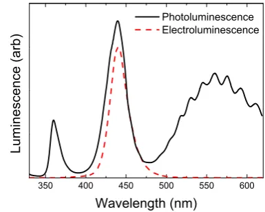
Figure 3 compares the room temperature PL from 230 nm diameter, vertically sided MQW nanorods formed after
KOH etching with the electroluminescence (EL) from an LED comprising an array of nanorods of the same diameter fabricated from the same wafer.13) The nanorods were
vertical sided, as shown in Fig. 1(c). Detailed micro-PL measurements on similar nanorods reported elsewhere14) revealed that the quantum well PL comprises several transitions closely spaced in energy. The hyperspectral CL imaging identifies a variation of the emission peak with position, resulting in a broadening of the macro-PL. In contrast, the EL peak is slightly narrower.
It is unclear if the broader PL peak derives from small differences in the confinement energy of the three QWs comprising the MQW, possibly due to different amounts of strain relaxation along the axis of the nanorods, or from other factors, for example strain relaxation along the radial direction of the nanorods arising from the formation of a free surface by the ICP etching.15)
In order to distinguish between these two possibilities nanorods containing only a SQW were fabricated in much the same way, apart from using ICP etch conditions optimised to form almost vertically sided structures.6) Figure 4(a) shows the CL intensity map obtained during hyperspectral CL imaging of an individual SQW nanorod from a 600 nm pitch hexagonal array of 290 nm diameter, 1000 nm high nanorods etched from a PIN GaN epitaxial layer containing a SQW. The lighter ring about half way up the nanorod shows the CL excited by a 10 kV beam of less than 20 nm diameter integrated across the QW emission band. Figure 4(b) shows the CL emission spectra at positions from edge to centre of the disk-shaped InGaN layer taken from the CL hyperspectral image. Point 1 corresponds to the outer edge of the nanorod whilst point 3 corresponds to aligning the electron beam to its centre, with point 2 approximately equidistant between these extremes.
Moving from point 1 to point 2 and on to point 3, the peak emission band shifts to higher photon energy by
[image:2.595.327.520.62.216.2]50meV. The QW emission band also broadens to higher energy. This is especially marked in the spectrum measured at point 3 which includes light emitted from the nanorod core. Kawakami et al. report a similar blue shift in QW
[image:2.595.60.279.63.239.2]Fig. 2. (Color online) Evolution of the room temperature peak of the MQW photoluminescence (left vertical axis) and its intensity (right vertical axis) with nanorod thinning by KOH etching.
photoluminescence from GaN nanorods of diameter 0.5– 2m containing a SQW.15) These authors interpreted their results in terms of two optical transitions occurring in the SQW: higher energy PL coming from the centre of the SQW which is still under compressive biaxial strain and a lower transition occurring in a ring of largely relaxed material around the nanorod outer diameter. The same model fits the behaviour observed in the 290 nm diameter nanorods reported here.
Figure 5 shows the CL spectra measured using similar beam conditions at three equivalent points on a 200 nm diameter nanorod containing a SQW. Again the emission peak from the centre of the nanorod is broadened compared with that from the edge. However, in this narrower nanorod the lower energy peak of the broadened spectrum remains dominant. This has the effect that the apparent blue shift in the emission band peak is much smaller than in the 290 nm nanorods of the same height (1m) fabricated from the same PI(SQW)N material.
If the radial penetration of the strain relaxation is the same in the 200 and 290 nm diameter nanorods, as is likely from mechanical considerations, then the strain relaxed outer shell of the narrower nanorod will comprise a larger fraction of the total volume of the InGaN QW layer. Consequently, the relative contribution of light emission from the strained core region of the 200 nm diameter nanorod will be smaller and the apparent blue shift in the overall emission peak will be smaller.
3.2 Simulation results
[image:3.595.320.525.61.220.2]The waveguide properties of a nanorod must be taken into account in assessing the relative contributions of the light emission from its core and strained relaxed outer shell. Figure 6 shows the variation in the power emitted by a Hertzian dipole into the vertically propagating guided and radiation modes of a nanorod as a function of the radial position of the dipole in (a) a 300 nm diameter and (b) a 200 nm diameter infinitely long GaN nanorod calculated
Fig. 5. (Color online) CL spectra measured using similar beam conditions at three equivalent points on a 200 nm diameter nanorod containing a SQW.
0 50 100 150
0 0.2 0.4 0.6 0.8 1
Distance of dipole from origin (nm)
Normalized power guided power
radiated power total power
(a)
0 20 40 60 80 100 0
0.2 0.4 0.6 0.8 1
Distance of dipole from origin (nm)
Normalized power
guided power radiated power total power
(b)
Fig. 6. Calculated variation in the contributions of the power in the vertically propagating guided and radiation modes of a nanorod as a function of the radial position of a dipole in infinitely long GaN nanorod of (a) 300 nm diameter and (b) 200 nm diameter.
(a)
[image:3.595.67.270.63.366.2](b)
[image:3.595.323.526.287.604.2]using a modal expansion method.16)The effect of aligning the dipole moment along or perpendicular to the radial direction is taken into account. A dipole emission wave-length of 460 nm has been used. The emitted power has been normalized so that ‘‘1’’ represents the power that would be emitted by a dipole of equal strength inside an infinite GaN medium.
These results show that, in the case of a 300 nm diameter nanorod, the fraction of the emitted power coupling into radiation modes is substantially higher when a dipole is located near the vertical edge of the nanorod, compared with when it is located near its core. On the other hand, in a 200 nm diameter nanorod dipoles located in the centre of the nanorod couple more strongly with radiation modes, but the variation in the coupling strength with radial position of the dipole is less marked than for 300 nm diameter nanorods. Thus, the extraction efficiency of light generated in the strain relaxed outer shell of quantum wells located in a nanorod is dependent on the diameter of the latter. This effect will contribute to the observed intensity of light emission from the InGaN disk in addition to the volume ratio of its compressively strained core and relaxed outer shell. Thus, the differences in the CL spectra in Figs. 4(b) and 5 are not simply due to volume differences as the nanorod diameter is reduced from 290 to 200 nm.
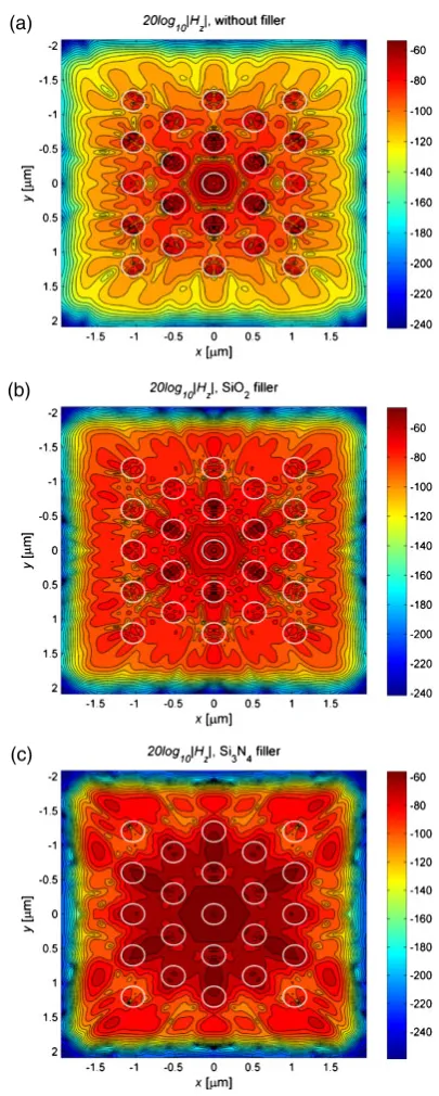
[image:4.595.325.528.58.564.2]Arrays of nanorod emitters are required for deployment in solid state lighting,17) opening the possibility that effects arising from the geometry of the array will influence measurements of light emission. FDTD simulations have been performed with spatial resolution of 25 nm for light emission from a hexagonal array of 300 nm diameter, 1m high nanorods containing a SQW located half way up the structure. The pitch of the hexagonal array was 600 nm and the emission wavelength was 450 nm. The point source (dipole) was located at the origin of the central nanorod of a 55 array. Incoherent behaviour was modelled by performing two separate simulations first with the dipole moment polarized along thex-axis and then they-axis, both in the plane of the SQW. The results for each polarization were then added incoherently.
Figure 7 shows the calculated near field pattern of the magnetic field component (in dB) along the vertical axis of the nanorods at a point 250 nm above the SQW for the cases of (a) air, (b) SiO2 and (c) Si3N4 filling the regions between the nanorods. The grey scale from black to white color scale online from blue to red corresponds to increasing field amplitude. For each filling the near field radiation pattern has a hexagonal symmetry and is periodic along the six principal axes of the nanorod array. Such behaviour is characteristic of Bloch mode formation in the plane of the nanorods. However, the modes giving rise to this behaviour rapidly decay via light either escaping into the layer of air above the structure or coupling into a 3-m-deep GaN buffer layer assumed in the simulation to lie directly below the nanorods.
As the refractive index of the infilling medium increases from unity for air to 2.05 in the case of Si3N4 the field spreading from the central nanorod into its nearest and second nearest neighbours becomes more marked. This is because the effective refractive index of the layer compris-ing the nanorods and filler is increased and the rate of
coupling of light into the buffer layer decreases. It is expected that light coupled into the guided modes of the buffer layer will then undergo diffraction as a consequence of the periodic refractive index variation arising from the presence of the nanorod array in the composite structure.
4. Conclusions
In summary, a wide ranging study of the optical properties of GaN nanorods containing either a three-well InGaN/GaN MQW or a single InGaN QW has been performed. The PL
(a)
(c) (b)
and CL spectra of single nanorods containing either a MQW or SQW comprise at least two dominant radiative transitions. Hyperspectral CL imaging of single nanorods containing a SQW revealed that the dominant lower energy transition originates from the outer shell of the InGaN layer, whilst the dominant higher energy transition comes from its core.
Analysis of the coupling of light into guided and radiation modes of a nanorod revealed that the extraction efficiency of light generated in the outer shell is higher or lower depending on the nanorod diameter and thus will bias the shape of the emission spectrum.
FDTD simulations reveal that light emitted from nanorods in an array with hexagonal symmetry can couple into waveguide modes with characteristics of Bloch modes. Finally, comparison of the PL and EL spectra in Fig. 3 of a prototype nanorod array LED reveals that the radial variation in the local potential in the InGaN SQW in a nanorod that gives rise to the different transitions is sensitive to the density of injected charge.
Acknowledgments
The authors wish to acknowledge support from the European Community’s Seventh Framework Programme FP7/2007– 2011 under grant agreement No. CP-IP 228999-2, project ‘‘SMASH’’ and from the UK Engineering and Physical Sciences Research Council, under grant EP/1012591.
1) H.-M. Kim, Y. H. Cho, H. Lee, S. I. Kim, S. Y. Ryu, D. Y. Kim, T. W. Kang, and K. S. Chung:Nano Lett.4(2004) 1059.
2) T. H. Hsueh, J. K. Sheu, H. W. Haung, Y. H. Chang, M. C. Ou-Yang, H. C. Kuo, and S. C. Wang:Jpn. J. Appl. Phys.44(2005) 7723.
3) L. Dai, B. Zhang, J. Y. Lin, and H. X. Jiang:J. Appl. Phys.89(2001) 4951. 4) J. Kupec, R. L. Stoop, and B. Witzigmann:Opt. Express18(2010) 27589. 5) M. Boroditsky, R. Vrijen, T. F. Krauss, R. Coccioli, R. Bhat, and E.
Yablonovitch:J. Lightwave Technol.17(1999) 2096.
6) P. A. Shields and D. W. E. Allsopp:Microelectron. Eng.88(2011) 3011. 7) X. A. Cao, S. J. Pearton, A. P. Zhang, G. T. Dang, F. Ren, R. J. Shul, L.
Zhang, R. Hickman, and J. M. Van Hove:Appl. Phys. Lett.75(1999) 2569.
8) P. R. Edwards and R. W. Martin:Semicond. Sci. Technol.26(2011) 064005.
9) A. Taflove and S. C. Hagness:Computational Electrodynamics: The Finite-Difference Time-Domain Method(Artech House, Norwood, MA, 2000).
10) A. F. Oskooi, D. Roundy, I. Mihai, B. Peter, J. D. Joannopoulos, and S. G. Johnson:Comput. Phys. Commun.181(2010) 687.
11) Z. Z. Bandic´, P. M. Bridger, E. C. Piquette, and T. C. McGill:Solid-State Electron.44(2000) 221.
12) Q. Wang, J. Bai, Y. P. Gong, and T. Wang:J. Phys. D44(2011) 395102. 13) P. A. Shields, C. Chan, N. Read, D. W. E. Allsopp, R. A. Taylor, and F. Causa: presented at OSA Meet. Solid State and Organic Lighting (SOLED 2010), 2010.
14) C. C. S. Chan, B. P. L. Reid, R. A. Taylor, Y. D. Zhuang, P. A. Shields, D. W. E. Allsopp, and W. Jia:Appl. Phys. Lett.102(2013) 111906. 15) Y. Kawakami, A. Kaneta, L. Su, Y. Zhu, K. Okamoto, M. Funato, A.
Kikuchi, and K. Kishino:J. Appl. Phys.107(2010) 023522.
16) A. W. Snyder and J. D. Love:Optical Waveguide Theory(Chapman and Hall, London, 1983) p. 520.