Integrated micro-spectrometer with elliptical Bragg mirror
enhanced diffraction grating on silicon on insulator
Pierre Pottier*,1, Michael J. Strain2,3, Muthukumaran Packirisamy1
1 Optical-Bio Microsystems Laboratory, Department of Mechanical & Industrial Engineering,
Concordia University, 1455 De Maisonneuve Blvd. West, Montreal, QC, H3G 1M8, Canada
2 Optoelectronics Research Group, School of Engineering, University of Glasgow, Rankine
Building, Oakfield Avenue, Glasgow G12 8LT, Scotland, UK
3 Institute of Photonics, Wolfson Centre, University of Strathclyde, Glasgow G4 ONW, Scotland,
UK
ABSTRACT: An on-chip micro-spectrometer is demonstrated based on a circular diffraction grating consisting of an elliptical Bragg mirror. This structure results in a highly efficient and compact device with simplified processing requirements, useful for sensing, spectroscopy, telecom demultiplexing, and optical interconnects. The computed efficiency for a realistic geometry is -0.14 dB, which represents to the best of our knowledge the highest predicted efficiency for concave diffraction gratings (echelle/echelette gratings). The first realization of the elliptical Bragg mirror diffraction grating spectrometer is presented on silicon on insulator at a wavelength of 1.55 µm. Measurements show a full device efficiency of -3.0 dB, including all in-line losses, with a band flatness of 0.4 dB over 30 nm.
KEYWORDS: planar spectrometer, diffraction grating, Bragg mirror, optical design, integrated optics
The integration of wavelength separation functionality on a chip using planar waveguide technology is at the heart of the development of optical components for telecommunications and sensing applications. This function is critical for optical wavelength division multiplexing (WDM) telecommunications schemes, which can significantly increase the capacity of optical networks.1 In a similar way, wavelength division filters can be used in optical interconnects to transmit data on or between chips, notably with silicon photonics.2 Integrated spectrometers can be created using the same basic technology, and used for spectroscopic measurements, such as for gas detection,3 molecule detection, optical coherence tomography (OCT),4 and astronomy.5 The application reach of integrated sensors is vast and is greatly enhanced by realizing the spectrometer operation on-chip, removing the necessity for processing measurement signals using large, expensive lab based devices. Furthermore, these sensor units can be monolithically integrated with complimentary lab-on-a-chip technologies,6,7 such as microfluidics, for more complex and efficient detection systems, or for cheaper or disposable units.
diffraction grating (CDG),8,11,14,16-25 often referred as echelle grating. The AWG consists of (i) an input waveguide, (ii) a laterally free propagation region where the beam expands and couples to (iii) an array of waveguides that exhibit variable path lengths and hence path phase differences, after which the waveguides are coupled to (iv) a second laterally free propagation region (star coupler) and recombine and focus into (v) a set of output waveguides that are discriminated in wavelength due to the accumulated phase profile in the waveguide array section.
The CDG operates using (i) an input waveguide coupled into (ii) a laterally free propagation region where the beam expands and reflects from (iii) a curved diffraction grating back into the same laterally free propagation region and recombines to focus into (iv) a set of output waveguides, with the wavelength dependence of the imaged plane related to the grating period, curvature and the propagation path length.
AWGs are widely used in optical telecommunications for WDM and though they have been demonstrated in silicon on insulator (SOI) and InP material platforms they are most commonly based on silica on silicon (SoS) technology, which provides good direct coupling to optical fibers but requires large bend radii. One of the most significant drawbacks in the use of AWGs is the large space occupied by the array of waveguides. This can be a limitation for high channel counts. Crosstalk is also an issue, arising from phase errors in the array of waveguides26-28 due to size irregularity in fabrication, and also from stray light generated at the connection between the laterally free propagation region and the array of waveguides. For CDGs, a drawback is the difficulty of obtaining a good vertical sidewall for the etched region through the core, defining the diffraction grating, which leads to increased losses. The use of a metallic mirror also absorbs some light20 and leads to polarization-dependent loss (PDL).11 But an important point is the reduction of size. Indeed, compared to AWGs, only one laterally free propagation region is present and, more importantly, no array of waveguides is present. The smaller size of the CDG device has several advantages. (i) Production of a more compact packaged device (e.g. for stand-alone spectrometer applications). (ii) A CDG can be added to a chip (e.g. microfluidic lab-on-a-chip diagnostic devices) without significantly altering the size of the device. (iii) The production cost reduces due to reduced foot-print. (iv) The yield or reliability increases as there will be less fabrication defects or nonuniformity due to smaller size. (v) The power requirement is lower if temperature control is needed, such as for tight wavelength control for WDM.
■ DESIGN
Geometry
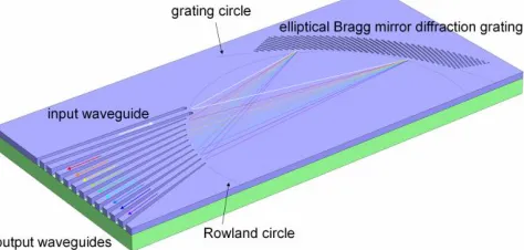
A classical configuration used for CDGs is the Rowland mounting,8,11 and is also the one adopted here. It consists of placing the access waveguide extremities on a circle of radius RRC (the
Rowland circle), and oriented towards the diffraction grating center (Figure 1). The diffraction grating itself has a radius of curvature of 2RRC, and is tangent to the Rowland circle (at the
[image:3.612.189.426.396.509.2]grating pole). This allows focusing of the input beam back to the output after reflection and diffraction on the grating. But in the present situation, the classical grating facets are replaced by elliptical Bragg mirrors whose foci are the input and central output waveguide extremities. The ellipses extend over and define the diffraction grating. This provides aberration-free focusing, blazing condition, and combines a high Bragg reflection with a grating diffraction. This almost facet-free diffraction grating allows, by managing diffraction orders, to redirect nearly all of the power into one output.31 In order to determine the suitable periodicity of the Bragg mirror diffraction grating configuration, three scenarios are discussed here. Case A consists of a constant periodicity of the Bragg mirror (Figure 2). Case B consists of a constant periodicity of the facet positions along a projection on a line tangent to the grating at its pole (this is the classical Rowland configuration). And case C has a constant periodicity of the facet positions along the grating circle. These three cases differ slightly and case A cannot be strictly satisfied simultaneously with case B or case C. But the three cases will become similar when the beam divergence is low and the Rowland circle radius is high, as the diffraction grating tends to be flat.
Figure 2. Spectrometer geometrical parameters and configurations of the elliptical Bragg mirror diffraction grating studied: case A: constant Bragg mirror period, case B: constant diffraction grating projected period (classical Rowland configuration), and case C: constant diffraction grating curvilinear period.
Equations and parameters
The two main equations governing the Bragg mirror diffraction grating are the grating equation
nasin sin
M (1)
and the Bragg condition
2 2 22 1 sin
cos 1 2 n n fn n f d
m , (2)
with λ the wavelength in vacuum, n the refractive index of medium, α the incident angle on diffraction grating, β the diffracted angle, M the diffraction order, a the period of the diffraction grating, m the Bragg order, d the Bragg period, f the filling fraction of material of index n2 in alternation with material of index n in the Bragg mirror, and φ the angle of incidence on the Bragg mirror31 (Figure 2). The other relations linking the parameters together are:
2
, (3)
2 sin
a
d , (4)
2
, (5)
with θ the angle between the Bragg elements and the grating front. Since we are using only two different materials (n and n2) and not three, the matching of (1) and (2) is not perfect (m ≈ -M)31 and will lead to a shift of the region of efficiency. The central operational wavelength is
λc = 1550 nm while the wavelength of the geometrical design is shifted to λ0 = 1600 nm due to
this reason. The angles are chosen as α = -45° and β0 = -43°. The index n used is the effective index neff = 2.849 of a silicon slab waveguide of thickness t = 220 nm and index nSi = 3.477,
surrounded by silica of index nSiO2 = 1.444, at the wavelength λc. A suitable design with high
efficiency was carried out, after taking care of the constraints of size in fabrication (d, f) and vertical losses (m, f). From this, results the choice of M = -2, a = 808.6 nm from (1) with above
neff and λ0, d = 561.7 nm from (4), and f = 0.14. We also get θ = 44° from (5) and φ = -1° from (3).
The wavelength spacing between channels was chosen as Δλ = 16 nm, with waveguides of width
w = 4 µm, which leads to RRC = 164 µm, with a spacing between output waveguides of ~0.6 µm.
Simulations
The micro-spectrometers are simulated with access waveguides, using the finite-difference time-domain (FDTD) method in a 2D fashion, using the effective index neff previously mentioned. The
polarization is TE (E in the plane of the slab, i.e. the simulation plane). The access waveguides are laterally confined with silica (index nSiO2), and the Bragg mirror diffraction grating is made of
elliptical grooves filled by silica (index n2 = nSiO2) alternating with the silicon (index n = neff). The
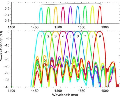
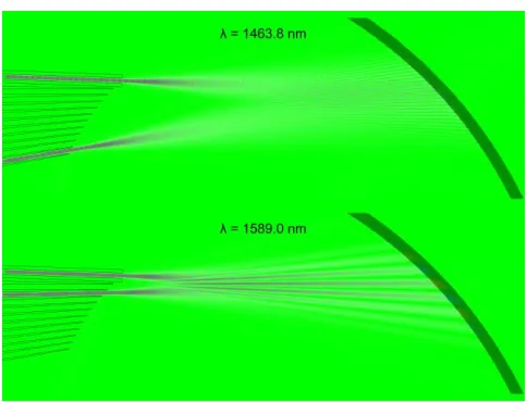
correspond to the micro-spectrometer efficiency, i.e. from input waveguide to output waveguides. Also shown is the power collected over all of the channels (in gray), but without the output waveguides present. This represents the efficiency of the diffraction grating for the diffracted order, without coupling losses into output waveguides. For case A (constant Bragg period), the diffraction grating efficiency is -0.011 dB, the spectrometer efficiency -0.10 dB, and the channel uniformity 0.07 dB over the 125 nm range. The next-channel crosstalk is -22 dB and the overall isolation -17 dB. For case B (constant projected diffraction grating period), the diffraction grating efficiency is -0.011 dB, with the spectrometer efficiency -0.06 dB, the channel uniformity 0.05 dB (over 125 nm), the next-channel crosstalk -23 dB, and the overall isolation -17 dB. First it can be noted that these efficiencies are very high, and of similar level, which shows both cases can be used. Case B behaves slightly better, as for case A the diffraction grating period cannot be kept exactly constant because the Bragg mirror period is itself fixed and the grating circular, so case B will focus more perfectly the whole beam of light into the output waveguide. The crosstalk present is due to the fact that the rounded tip at the separation between two output waveguides redirects a small portion of light to the other output waveguides. It can be enhanced by careful design of the connection region (possibly including tapers). Without such optimization yet, the coupling losses from the free beam (laterally free propagation region) to output waveguides is 0.10 dB for case A and 0.05 dB for case B. A further improvement is also expected by slightly shifting the Bragg mirror diffraction grating towards the input and output waveguides to compensate for penetration depth into the Bragg mirror. Concerning case C, the results are less good, with a diffraction grating efficiency of -0.026 dB, a spectrometer efficiency of -0.47 dB, and a next-channel crosstalk of -10 dB. The focusing back to output waveguides has degraded, as can be seen with the broadening of peaks. A movie representing the distribution of light in the spectrometer as the wavelength is changed is presented in the Supporting Information displayed in Figure 6 for case B, and shows clearly the efficient separation of wavelengths in the different output channels. This distribution of light is also shown in Figure 6, for two wavelengths.
Figure 4. Power efficiency spectra (multicolor) in output channels of a micro-spectrometer using an elliptical Bragg mirror diffraction grating having a constant projected diffraction grating period (case B, classical Rowland grating). The total power collected over all the channels, before coupling into them, is represented in gray.
[image:6.612.199.405.329.495.2]Figure 6. Distribution of light in the micro-spectrometer for two different wavelengths, showing the separation in different channels. A movie covering the full wavelength range is also presented in the Supporting Information.
Bragg mirror losses
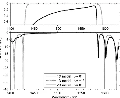
For a full estimation of efficiency of the spectrometer, the losses that take place in the Bragg mirror in the third dimension also need to be computed. The Bragg mirror contains 20 periods, with alternation of silica (length fd = 78.6 nm) and silicon slab waveguide (length (1-f)d = 483.1 nm). An initial computation with a 1D model,32 using indices nSiO2 and neff for the
alternating components, shows a bandwidth of high reflection from 1440 to 1580 nm (Figure 7), with results almost identical for normal incidence (φ = 0°) and the incidence used in the spectrometer (φ = -1°) (p-polarization). This region of high reflection corresponds closely to the region of high efficiency of the diffraction grating. Then a 2D FDTD simulation of a vertical cross-section of the Bragg mirror (necessarily at φ = 0°) is carried with indices nSiO2 and nSi for
Figure 7. Reflection of the Bragg mirror used in the micro-spectrometer diffraction grating, with a 1D model, and a 2D model including the losses.
Combined with the previous results of the horizontal 2D spectrometer, these vertical 2D Bragg mirror results allow the estimation of the full micro-spectrometer device efficiency in a realistic situation. This efficiency is -0.14 dB (97 %), which represents the highest value predicted for any CDG design to the best of our knowledge. In terms of usage over a certain range of wavelengths, an example is the fiber-optic communication C-band (1530-1565 nm), for which the micro-spectrometer presents an insertion loss of 0.26 dB with a channel uniformity of 0.09 dB. For comparison, a classical CDG presents an efficiency of about -3.3 dB,22,33 and with an optimized design -1.9 to -1.1 dB.20,22,33 Note that attention should be paid on what is exactly estimated (facet, grating, curved grating, full spectrometer with access waveguides) and the approximation of the method used.
Dispersion
The silicon slab waveguide used for the spectrometer presents a dispersion which has not been yet taken into account in the design. The effect on the angular dispersion of the diffraction grating can be calculated and therefore the resultant channel spacing of the spectrometer. By differentiating the grating equation (1), one gets the angular dispersion
2 cos n n a M d d
Dd g
, (6)
where d dn n
ng (7)
is the group index. For a non-dispersive waveguide situation, the angular dispersion is
cos
na M
Dnd . (8)
The ratio of dispersive to non-dispersive channel wavelength spacing is therefore
d gnd nd d n n D D
In the present design, ng = 3.578 (at λc). This leads to a channel spacing ratio of 0.796. Initially
designed for a channel spacing of Δλ = 16 nm (non-dispersive slab waveguide), the spectrometer will actually have a channel spacing of (Δλ)d = 12.7 nm. When the waveguides used are thick, e.g.
SoS technology matching with optical fibers, the difference is negligible, but when the waveguides are thin, such as with silicon nanophotonics, it has to be taken into account, and can even be taken as an advantage, by providing more angular wavelength dispersion and therefore lower channel spacing in the case of a demultiplexer or higher wavelength resolution in the case of a spectrograph.
■ FABRICATION AND MEASUREMENT
Fabrication
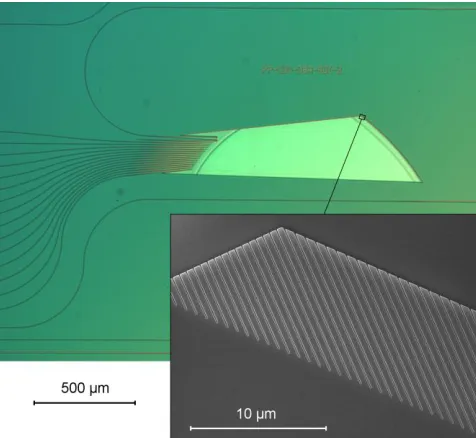
A micro-spectrometer was realized on a standard SOI material platform with a waveguide core thickness of 220 nm and a buried oxide layer of 2 µm. The waveguides, the laterally free propagation region, and the diffraction grating were patterned in hydrogen silsesquioxane (HSQ) resist using electron-beam lithography, which was then used as a mask for the dry etching of silicon down to the oxide, with inductively coupled plasma (ICP) reactive ion etching (RIE) using SF6/C4F8 gas. The structures were then covered by a 900 nm thick silica layer. A SEM image of a section of the elliptical Bragg mirror diffraction grating is presented in the inset of Figure 8.
Figure 8. Fabricated micro-spectrometer with access waveguides on SOI, with in inset the elliptical Bragg mirror diffraction grating etched in silicon.
[image:9.612.187.425.389.608.2]with the Rowland circle radius readjusted consequently, due to computation limitations. It can be expected that the configuration used in fabrication will give very similar and even slightly better results in simulation since the diffraction grating has the same optical characteristics, but is even flatter. The output waveguides include an S-bend section to provide separation at the chip facet, and the input waveguide includes a U-turn section to be accessed by the opposite chip facet (Figure 8). The minimum radius of curvature of bends is 320 µm. In the waveguide straight sections and bends, the width is w2 = 0.5 µm to maintain single mode propagation. There is then a taper between these access waveguides and the waveguide extremities on the Rowland circle, and another taper at the chip facet to improve off-chip coupling to fiber. These two kinds of tapers are linear, and respectively 350 µm and 200 µm long, i.e. for the 0.5 to 8 µm and the 0.5 to 4 µm. Their efficiency has also been simulated (2D FDTD) and is respectively -0.017 dB (99.6 %) and -0.013 dB (99.7 %) (over the wavelength range 1450-1650 nm), therefore introducing negligible losses.
Optical testing
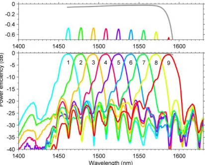
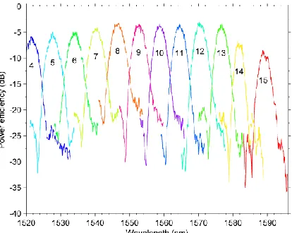
The micro-spectrometer efficiency was measured on an optical bench using polarization maintaining optical fiber, with TE input polarization. The source of light is a tunable laser and the spectra are acquired on an optical spectrum analyzer (OSA). High resolution scanning of the source is performed at a wavelength step of 0.01 nm, while recording the maxima on the OSA with a resolution bandwidth of 0.2 nm. In this way, we are measuring the envelope of the transmission curve only, which otherwise contains strong Fabry-Perot oscillations very closely spaced (~0.07 nm) due to internal reflection at the two facets and which prevents accurate normalization. The spectrometer spectra are normalized to a reference 2×90° S-bend waveguide with the same waveguide characteristics and chip access tapers as those used for the spectrometer. Therefore what is measured is the whole spectrometer efficiency, from input to output 0.5 µm waveguide, and it includes any losses possibly arising from: Rowland circle taper losses, waveguide to slab coupling, waveguide or slab propagation losses, diffraction grating losses, and Bragg mirror losses. The micro-spectrometer efficiency spectra are displayed in Figure 9, and show an efficiency of -3.0 dB (50 %). The gradual decrease of efficiency at low wavelengths is probably due to the Bragg mirror vertical losses which have shown such tendency in the simulation, and the decrease of efficiency at high wavelengths seems also due to the Bragg mirror which is at the stopband edge (Figure 7). A good channel uniformity (0.4 dB) is present in the middle of the range (channels 8-13) over a band of 30 nm. The crosstalk was also measured, with a next-channel crosstalk of -15 dB, and an overall isolation of -14 dB. As stated in the simulation section, this can be further improved with precise design of the coupling back to output waveguides. There is also possibly stray light reflecting on the boundaries of the laterally free propagation (slab) region and entering output waveguides, deteriorating the crosstalk. This region was limited in extent to reduce the negative lithography exposure time, but could be modified in shape or extended to the whole chip to reduce stray light. The measured channel spacing is 6.1 nm and it matches closely with the expected (Δλ)d = 0.796 × 8 nm = 6.37 nm, knowing
0.2 dB.14,19-21,24,25,29,30,33-35 This places the present spectrometer within the state of the art for efficiency and at a high level for uniformity. Moreover its efficiency can still be improved, whereas other CDG devices are limited by the design.
Figure 9. Experimental power efficiency spectra (multicolor) of the channels of the micro-spectrometer realized on SOI using an elliptical Bragg mirror diffraction grating.
■ CONCLUSION
An on-chip micro-spectrometer with elliptical Bragg mirror concave diffraction grating has been demonstrated on SOI. Thanks to the specific design of the diffraction grating, it has been shown through precise computation that a single order of diffraction can be generated and efficiently coupled back to output waveguides, resulting in a record global efficiency of -0.14 dB (97 %) for the whole spectrometer (including vertical losses). The first implementation of this device was presented for silicon photonics, with state of the art experimental results, showing an efficiency of -3.0 dB and a high band flatness (0.4 dB). It is now possible to refine all the elements still contributing to losses, such as access waveguides, transition regions, etc., as has been carried out for other micro-spectrometers or demultiplexers, in order to achieve the predicted efficiency. [alternative sentence: All the refinements that have been carried out for other micro-spectrometers or demultiplexers, such as access waveguides, transition regions, etc., can now be applied to the present device in order to tackle the remaining losses and achieve the predicted efficiency.] The present design offers here a full potential, where other CDG devices are limited by design. This enables very compact and at the same time very efficient spectrometers, desired in many applications such as sensing and optical routing.
■ AUTHOR INFORMATION
[image:11.612.199.406.135.300.2]■ ACKNOWLEDGMENTS
The authors would like to thank the Natural Sciences and Engineering Research Council of Canada (NSERC) Discovery Grants and Concordia Research Chair of M. Packirisamy, the James Watt Nanofabrication Centre (JWNC), as well as Richard M. De La Rue and Marc Sorel for their support.
■ SUPPORTING INFORMATION
Movie representing the distribution of light in the micro-spectrometer, as the wavelength is changed, and showing the separation in the different output channels. This material is available free of charge via the Internet at http://pubs.acs.org/photonics.
■ REFERENCES
1. Tomlinson, W. J. Wavelength multiplexing in multimode optical fibers. Appl. Opt. 1977,
16, 2180-2194.
2. Miller, D. A. B. Device Requirements for Optical Interconnects to Silicon Chips. Proc. IEEE 2009, 97, 1166-1185.
3. Yebo, N. A.; Bogaerts, W.; Hens, Z.; Baets, R. On-Chip Arrayed Waveguide Grating Interrogated Silicon-on-Insulator Microring Resonator-Based Gas Sensor. IEEE Photonics Technol. Lett. 2011, 23, 1505-1507.
4. Nguyen, V. D.; Akca, B. I.; Wörhoff, K.; de Ridder, R. M.; Pollnau, M.; van Leeuwen, T. G.; Kalkman, J. Spectral domain optical coherence tomography imaging with an integrated optics spectrometer. Opt. Lett. 2011, 36, 1293-1295.
5. Cvetojevic, N.; Jovanovic, N.; Lawrence, J.; Withford, M.; Bland-Hawthorn, J. Developing arrayed waveguide grating spectrographs for multi-object astronomical spectroscopy. Opt. Express 2012, 20, 2062-2072.
6. Kodate, K.; Komai, Y. Compact spectroscopic sensor using an arrayed waveguide grating.
J. Opt. A: Pure Appl. Opt. 2008, 10, 044011.
7. Hu, Z.; Glidle, A.; Ironside, C. N.; Sorel, M.; Strain, M. J.; Cooper, J.; Yin, H. Integrated microspectrometer for fluorescence based analysis in a microfluidic format. Lab Chip
2012, 12, 2850-2857.
8. Hutley, M. C. Diffraction Gratings (Techniques of Physics: 6). Academic Press: London, 1982.
9. Si, Y. C.; Cheng, Y. Optical Multiplexer/Demultiplexer: Discrete. In WDM Technologies, Vol. II: Passive Optical Components; Dutta, A. K., Dutta, N. K., Fujiwara, M., Eds.; Academic Press: San Diego, 2003; Ch. 3.
10. Smit, M. K. New focusing and dispersive planar component based on an optical phased array. Electron. Lett. 1988, 24, 385-386.
12. Fukazawa, T.; Ohno, F.; Baba, T. Very compact arrayed-waveguide-grating demultiplexer using Si photonic wire waveguides. Jpn. J. Appl. Phys. 2004, 43, L673-L675.
13. Barbarin, Y.; Leijtens, X. J. M.; Bente, E. A. J. M.; Louzao, C. M.; Kooiman, J. R.; Smit, M. K. Extremely Small AWG Demultiplexer Fabricated on InP by Using a Double-Etch Process. IEEE Photonics Technol. Lett. 2004, 16, 2478-2480.
14. Bogaerts, W.; Selvaraja, S. K.; Dumon, P.; Brouckaert, J.; De Vos, K.; Van Thourhout, D.; Baets, R. Silicon-on-Insulator Spectral Filters Fabricated With CMOS Technology.
IEEE J. Sel. Topics Quantum Electron. 2010, 16, 33-44.
15. Fang, Q.; Liow, T.-Y.; Song, J. F.; Ang, K. W.; Bin Yu, M.; Lo, G. Q.; Kwong, D.-L. WDM multi-channel silicon photonic receiver with 320 Gbps data transmission capability.
Opt. Express 2010, 18, 5106-5113.
16. Soole, J. B. D.; Scherer, A.; LeBlanc, H. P.; Andreadakis, N. C.; Bhat, R.; Koza, M. A. Monolithic InP/InGaAsP/InP grating spectrometer for the 1.48-1.56 µm wavelength range.
Appl. Phys. Lett. 1991, 58, 1949-1951.
17. Cremer, C.; Ebbinghaus, G.; Heise, G.; Müller-Nawrath, R.; Schienle, M.; Stoll, L. Grating spectrograph in InGaAsP/InP for dense wavelength division multiplexing. Appl. Phys. Lett. 1991, 59, 627-629.
18. Clemens, P. C.; März, R.; Reichelt, A.; Schneider, H. W. Flat-Field Spectrograph in SiO2/Si. IEEE Photonics Technol. Lett. 1992, 4, 886-887.
19. Janz, S.; Balakrishnan, A.; Charbonneau, S.; Cheben, P.; Cloutier, M.; Delâge, A.; Dossou, K.; Erickson, L.; Gao, M.; Krug, P. A.; Lamontagne, B.; Packirisamy, M.; Pearson, M.; Xu, D.-X. Planar Waveguide Echelle Gratings in Silica-On-Silicon. IEEE Photonics Technol. Lett. 2004, 16, 503-505.
20. Bidnyk, S.; Balakrishnan, A.; Delâge, A.; Gao, M.; Krug, P. A.; Muthukumaran, P.; Pearson, M. Novel Architecture for Design of Planar Lightwave Interleavers. J. Lightwave Technol. 2005, 23, 1435-1440.
21. Horst, F.; Green, W. M. J.; Offrein, B. J.; Vlasov, Y. Echelle grating WDM (de-)multiplexers in SOI technology, based on a design with two stigmatic points. Proc. SPIE
2008, 6996, 69960R.
22. Lycett, R. J.; Gallagher, D. F. G.; Brulis, V. J. Perfect Chirped Echelle Grating Wavelength Multiplexor: Design and Optimization. IEEE Photonics J. 2013, 5, 2400123. 23. He, J.-J.; Lamontagne, B.; Delâge, A.; Erickson, L.; Davies, M.; Koteles, E. S. Monolithic
Integrated Wavelength Demultiplexer Based on a Waveguide Rowland Circle Grating in InGaAsP/InP. J. Lightwave Technol. 1998, 16, 631-638.
24. Muneeb, M.; Chen, X.; Verheyen, P.; Lepage, G.; Pathak, S.; Ryckeboer, E.; Malik, A.; Kuyken, B.; Nedeljkovic, M.; Van Campenhout, J.; Mashanovich, G. Z.; Roelkens, G. Demonstration of Silicon-on-insulator mid-infrared spectrometers operating at 3.8μm.
Opt. Express 2013, 21, 11659-11669.
25. Pello, J.; Muneeb, M.; Keyvaninia, S.; van der Tol, J. J. G. M.; Roelkens, G.; Smit, M. K. Planar Concave Grating Demultiplexers on an InP-Membrane-on-Silicon Photonic Platform. IEEE Photonics Technol. Lett. 2013, 25, 1969-1972.
28. Klekamp, A.; Münzner, R. Imaging errors in arrayed waveguide gratings. Opt. Quantum Electron. 2003, 35, 333-345.
29. Brouckaert, J.; Bogaerts, W.; Selvaraja, S.; Dumon, P.; Baets, R.; Van Thourhout, D. Planar Concave Grating Demultiplexer With High Reflective Bragg Reflector Facets.
IEEE Photonics Technol. Lett. 2008, 20, 309-311.
30. Jafari, A.; Kirk, A. G. Demonstration of Distributed Etched Diffraction Grating Demultiplexer. IEEE Photonics J. 2011, 3, 651-657.
31. Pottier, P.; Packirisamy, M. Design and Properties of Concave Diffraction Gratings Based on Elliptical Bragg Mirrors. J. Lightwave Technol. 2013, 31, 1890-1898.
32. Larouche, S.; Martinu, L. OpenFilters: open-source software for the design, optimization, and synthesis of optical Filters. Appl. Opt. 2008, 47, C219-C230.
33. Feng, D.; Qian, W.; Liang, H.; Kung, C.-C.; Fong, J.; Luff, B.J.; Asghari, M. Fabrication Insensitive Echelle Grating in Silicon-on-Insulator Platform. IEEE Photonics Technol. Lett. 2011, 23, 284-286.
34. Ryckeboer, E.; Gassenq, A.; Muneeb, M.; Hattasan, N.; Pathak, S.; Cerutti, L.; Rodriguez, J.B.; Tournié, E.; Bogaerts, W.; Baets, R.; Roelkens, G. Silicon-on-insulator spectrometers with integrated GaInAsSb photodiodes for wide-band spectroscopy from 1510 to 2300 nm. Opt. Express 2013, 21, 6101-6108.
35. Malik, A.; Muneeb, M.; Shimura, Y.; Van Campenhout, J.; Loo, R.; Roelkens, G.; Germanium-on-silicon planar concave grating wavelength (de)multiplexers in the mid-infrared. Appl. Phys. Lett. 2013, 103, 161119.