Abstract— We report on the modeling and testing of a Vernier latched MEMS variable optical attenuator (VOA) which uses chevron electrothermal microactuators to control fiber-to-fiber optical power coupling. The use of microlatches has the advantage of holding the mechanical position of the fiber, and therefore the level of attenuation, with no electrical energy supplied except only to change the attenuation. Results of analytical electro-thermo-mechanical models of the device have been obtained and compared with experimental test results, showing a good agreement. A step resolution of 0.5 μm for this multi-state latched device was achieved using a Vernier latch approach. This incremental step size is smaller than previously reported latched microactuators. The VOA demonstrated an attenuation range of over 47 dB and an insertion loss of 1 dB. The wavelength dependent loss across the optical communications C-band was 1.4 dB at 40 dB attenuation and the 10%-90% transition time of the unlatched VOA was measured to be 1.7 ms.
Index Terms— Variable optical attenuator, Fiber-to-fiber coupling, Vernier-latch, Electro-thermal actuators, Chevron microactuators.
I. INTRODUCTION
n fiber optic networks employing wavelength division multiplexing (WDM) protocols, the variable optical attenuator (VOA) is a crucial element for power equalization at transmission nodes, gain flattening in optical amplifiers, channel balancing at multiplexing points, and power management at receiving nodes. Due to the diverse power levels found in modern optical networks VOAs are required to operate over a large attenuation range, as well as having a low insertion loss (around 1 dB) and low wavelength dependent loss (WDL). In addition, the VOA should ideally have a linear operation over the attenuation range, be compact, low cost, and have a response time fast enough not to be detrimental to the network operation. In a dynamic network there is a desire to multiplex channels in a time of 1ms or less [1]. Here MEMS architectures can offer advantages over traditional bulk VOAs which can operate over a 50 dB attenuation range but have a slow response time of around 1 second. An early MEMS VOA reported by Ford et al. in 1998 [2] achieved 31
Manuscript received xxxxx xxxxx
A. Unamuno was with Centre for Microsystems and Photonics, University of Strathclyde. He is now with Fraunhofer IPMS, Dresden, Germany.
R. Blue and D. Uttamchandani are with the Centre for Microsystems and Photonics, University of Strathclyde, G1 1XW, U.K. (e-mail: [email protected]).
dB attenuation with a response time of 3 μs, demonstrating the potential of MEMS technologies to control light throughput in a network with little to no wavelength dependency. Since then a range of MEMS VOAs have been reported in the literature [3] from which three general methodologies can be identified: shutter type, reflective type, and fiber-to-fiber misalignment type.
Shutter type MEMS VOAs, which block the light path between a sending and a receiving fiber using one or more opaque shutters, have been demonstrated using electrostatic and electrothermal actuation with an attenuation range up to 30 dB [4]-[7]. In general the advantage of this type of MEMS VOA is its simplicity. A more complex shutter VOA was demonstrated by Syms et al. [8] using a series of shutter blades driven synchronously by separate microactuators to form an iris-type aperture yielding an optical attenuation of over 17 dB with a response time of 5 ms. An improved attenuation of 44 dB at 1550 nm was obtained using a sliding shutter driven by a scratch drive actuator [9].
Reflective mirrors based MEMS VOAs use micromirrors to steer light from a sending to a receiving fiber and the mirror tilt causes a controlled variation in the optical power coupling. A chevron type microactuator was used in a novel micromechanism to demonstrate 30 dB attenuation at 7.5 volts driving voltage [10]. A rotary comb microactuator moved a V-shaped mirror to give a maximum attenuation of 45 dB with response time less than 5 ms [11]. Curved micromirrors are used to obtain a more linear attenuation versus mirror position characteristic. Cai et al. [12] used a micromachined elliptical mirror to achieve a nearly linear relationship over a 30 dB attenuation range, and over a 100 nm wavelength range the WDL was 1.2 dB at the 20 dB attenuation level. Zhang et al. [13] reported a three-dimensional optical coupling design employing a pair of parabolic mirrors to obtain a linear relationship over a 62 dB range with an insertion loss of only 0.6 dB. More recently, Koh et al. [14] used an arrangement of 1x10 piezoelectric thin-film cantilever beam actuators fixed to one side of a square micro-mirror that allowed the mirror to move in six degrees of freedom. In front of the mirror a dual fiber core collimator was situated allowing light from the input fiber to be reflected off the mirror and back into the output fiber. By manipulating the actuators, a three dimensional attenuation mechanism took place which demonstrated a 40 dB attenuation range at 1 volt. Later the same authors improved upon this result by combining four sets of electrothermal actuators along the sides of the mirror together with actuation via electromagnetic coils in the frame around
Modeling and Characterization of a Vernier Latching
MEMS Variable Optical Attenuator
Anartz Unamuno, Robert Blue,
Member, IEEE
, and Deepak Uttamchandani,
Senior Member, IEEE
the mirror [15] to achieve a 40 dB attenuation for 17 mW of power consumption.
The third type of MEMS VOA is based on fiber-to-fiber coupling loss with controlled misalignment between two end-facing fibers, and involves moving the position of one of the optical fiber end faces with respect to the second fiber end face. One potential advantage of this format compared to the shutter and reflective mirror types is that there are no moving parts between the end-faces of the optical fibers that could vibrate and cause fluctuations in the optical attenuation. A second possible advantage of this format is that the end faces of the input and output fibers can be separated by as little as a few tens of microns because there is no mechanical component placed between the end faces of the fibers. This means that the insertion loss can be lower compared to other designs. For example, Dai et al. [16] described a MEMS VOA incorporating fiber-to-fiber lateral offset and reported an insertion loss of 0.68 dB. This low insertion loss is comparable to the best reported for VOA’s using reflective mirrors [13] but with, in general, reduced complexity. In addition, Hoffmann and Voges [17] reported a moving fiber-to-fiber bistable switch with an insertion loss <0.5 dB, demonstrating the potential for low insertion loss optical devices using a fiber-to-fiber format without intermediate optics.
Electrothermal microactuators are known for their large displacement and higher force output compared to their electrostatic counterparts making them suitable for this type of moving fiber VOA format [18]. Examples of this category are a microswitch with a channel isolation of 55 dB [19], and the work of Syms et al. [20] who described the use of folded buckling type electrothermal microactuators to form a bi-directional fiber alignment device, and demonstrated a prototype VOA with a 21 dB attenuation and low WDL.
Once the desired optical coupling (i.e. attenuation level) is achieved, the addition of a latching mechanism would be very useful to enable the mechanical position to be held with no electrical energy input requirement. The most common latched devices reported in the literature are bistable systems. This bi-stability can be achieved by buckling of beams which belong to the actuation mechanism [21], adding extra buckling beams [22] or using permanent magnetic fields combined with electrical signals to change between stable states [23]. However, these latching mechanisms have only two stable states. This is insufficient for applications such as VOAs where multiple latching states, with small displacements between two consecutive stable states, is required in order to ensure accurate control over the transmitted optical power. However, there are only a few publications demonstrating multi-state latched systems. Such latched microactuator systems have been implemented in chevron-latch [24] and chevron-peg [25] mechanisms. A shutter-based latched VOA driven by electrothermal shape bimorph actuators was described by Syms et al. [5] and used an optical lever format in conjunction with a conventional rack-and-tooth mechanism yielding a discrete set of attenuation states over a 30 dB range through 1 μm incremental steps of the shutter.
The latching step-size produced by a conventional rack-and-tooth latching system is determined by the feature size which the lithography and fabrication processes yield. In contrast, even though facing the same fabricated feature limitations of the conventional rack-and-tooth approach, a Vernier latch will generate higher step resolution achieved through its design. Multi-micron size fabricated features can generate a few and sub-micron steps following the Vernier approach. The principle of a Vernier method on a MEMS platform was demonstrated in strain sensors [26] and was later applied by Syms et al. [27] for precision alignment of MEMS rotation and translation stages beyond that which fabrication offers.
In this paper we present an alternative design of a highly accurate VOA operating over a 47 dB range to meet the needs of the telecoms community. The design, detailed electro-thermo-mechanical modeling and experimental results obtained from this latched VOA using a different Vernier based rack-and-tooth approach are reported here. Chevron-Vernier-latch combination achieves (in comparison to previously reported latched platforms) an improved resolution of 0.5 μm increment positional steps, which allows much finer control of the optical attenuation to be achieved.
II. VOADESIGN AND OPERATING PRINCIPLE
The attenuation mechanism used here is based on a fiber-to-fiber misalignment micro-structure fabricated using a chevron type electrothermal microactuator array detailed in [28]. The complete layout of the chevron actuator system forming a variable optical attenuator is shown in Figs. 1a and 1b. Two channels with spring-clips were designed to accommodate two single mode optical fibers facing each other with one fiber fixed and the other fiber cantilevered so that its tip was movable. By applying a lateral misalignment between the fibers the optical power transmitted between the fibers is controllably attenuated.
resolution using the layout shown in Fig. 1b, thereby yielding higher optical step resolution in the VOA response.
(a)
(b)
Fig. 1. (a) Layout of the MEMS device highlighting the location of the Vernier latching mechanism. (b) Close-up of latching mechanism shown in (a).
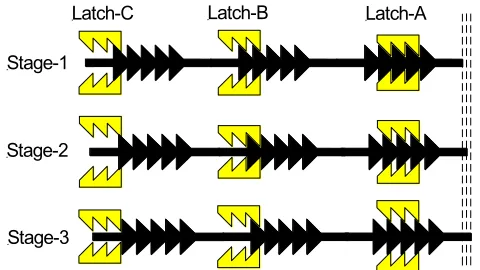
The Vernier principle applied here makes use of a cascaded set of latching cells as illustrated in Fig 2. The arrangement has a resolution of P/n where 'P' is the tooth-to-tooth distance, and 'n' is the number of latches. For example, if P = 10 µm and n = 3, then a resolution of 3.33 µm would be obtained, which would be implemented as a distance offset between Latch-A, Latch-B and Latch-C in Fig 2. In each stage shown in Fig. 2 a different latch is fully engaged (i.e. Stage 1 is Latch-A engaged, Stage2 is Latch-B engaged and Stage3 is Latch-C engaged), whereas the other two latches during each stage contribute to supporting the position by means of friction.
Latch-C Latch-B Latch-A
Stage-1
Stage-2
[image:3.612.317.557.70.205.2]Stage-3
Fig. 2. Principle of operation of the Vernier latching system.
There are various implementations of the latching principle and the arrangement finally selected (after several design iterations) is depicted in the 3D view of Fig. 3 where shape-bimorph actuators (Guckel actuators [29]) are used as the latch actuators which engage and disengage the latches. The dimensions of the actuators used are shown in Fig. 4, which is a finite element simulation of the shape-bimorph electrothermal actuator. The simulation results indicate that the actuator of these dimensions would require 3.4 volts and a current of 215 mA to move over 5 μm and disengage the latching teeth.
[image:3.612.52.299.92.553.2] [image:3.612.317.562.377.545.2]Fig. 4. Simulation result of the shape-bimorph actuator at 3.4 V and 215 mA.
The presence in our design of ten latches per branch and two offset branches as described earlier (n = 20) requires that all the latch actuators are simultaneously actuated. The device was fabricated on a SOI wafer with a single silicon layer for both device and electrical connections. Electrical connections to the latches were in series (as shown in Fig.3) so that current runs from Pad1 to Pad’1 and Pad2 to Pad’2. Fig. 5 shows photographs depicting stages of latching of one branch following actuation.
Fig 5 Photographs showing a sequence of latching motion on one branch of the mechanism.
III. CHEVRON MICROACTUATOR MODELING
Many designs of MEMS actuators can be found in the literature, reviewed in [30]. Electrothermal microactuators can be considered as key components for MEMS devices requiring large actuation forces [31]. The displacement and force generated by these actuators are in the order of tens of μm and
1 mN respectively [32, 33], although it is well noted that in certain applications they will require high power (>5 W [19]).
The principle for generating a deflection/force using thermal actuators is the expansion of the actuator structure due to the heat absorbed or internally generated. Micro-devices based on this phenomenon have been modeled and reported several times with different perspectives [34]-[38]. Microactuator modeling of the chevron microactuators (sometimes called ‘bent beam’ microactuators) used in our latching VOA is described in the following section.
Analytical modeling was performed to determine the temperature distribution and the resulting mechanical displacement of a chevron microactuator cluster. The electrothermal part of the analysis was separated from the thermomechanical analysis. This assumes that there is no temperature difference of the surroundings (i.e. air, substrate) at the different locations the device could be displaced to. The results obtained from the modeling are later compared with experimental results. The nomenclature, device dimensions and material characteristics used for model development are shown in Table I and a schematic illustration (not to scale) of a single actuator element of a chevron array is shown in Fig. 6. The two beams making up each element are anchored at their far ends and are connected to each other via a “shuttle”. We define L1 as the half beam length and the actuator full beam length is equal to 2L1. Both half beams are inclined at an initial “rake” angle of θ0. Upon actuation the shuttle is displaced a distance Δy.
Fig 6 Sketch of a pair of beams forming a single beam component of the chevron microactuator (not to scale).
TABLEI
NOMENCLATURE, DIMENSIONS AND MATERIAL CHARACTERISTICS Parameter Description Value w1 Width of Si beam 20 μm
w2 Width of middle Si beam 100 μm
L1 Half length of Si beam 3000 μm
L2 Length of middle Si beam 20 μm
t Thickness of Si 80 μm tAu Thickness of Au-Cr 0.65 μm [44]
tair Thickness of air 2 μm
kair Thermal conductivity of air 0.026 W/m - K
k Thermal conductivity of Si 148 W/m - K ξ Resistivity thermal coeff of Au 3.4x10⁻³ K-1
Ks Correction for shape factor 0.4
E Young’s modulus of (100) Si (depends on angle with respect to wafer primary flat)
See section III.B
αSi Thermal expansion coeff of Si 2.7 μm/m - K
at 40°C [45]
ρ0 Measured resistivity of Cr-Au on
silicon (room temp)
[image:4.612.317.563.399.476.2] [image:4.612.325.546.530.725.2]Although the silicon provided by the foundry was slightly doped, the resistivity of the silicon was still high (1-10 Ω-cm) compared to the measured resistivity of the gold (i.e. Cr-Au) on silicon (37.6 nΩ-m). For a 6 mm full length beam of width 20 µm with a 650 nm layer of gold this translates to a resistance of 17.4 Ω for the gold layer and at least 37.5 kΩ for Si. The current will therefore flow almost exclusively through the gold layer and thus we quote the resistivity of gold in Table I and this was used in the modeling.
A. Electrothermal model
The thermal model of the chevron microactuators was obtained by solving the basic one-dimensional heat transfer expressions. Three ways of heat transfer are possible: conductivity, convection and radiation. For simplification of the analysis in this paper, we have taken conductivity to be the only heat transfer mechanism. Hickey et al. [34] and Enikov et al. [38] have also considered conductivity as the only heat transfer mechanism in their modeling work, yielding good agreement between their analysis and experiments. As will be shown later, we have also obtained good agreement between results of our simplified analysis and experiments.
As already stated, most of the injected electric current will travel through the gold layer due to the very large electrical resistance difference between the gold and the underlying silicon layer. The model was therefore built assuming that all the heat is generated in the gold layer and transferred to the silicon layer by conduction.
Heat loss by conduction is expressed by (1)
therm s s cond
R
T
T
SdA
dq
(
)
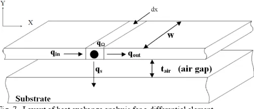
(1) [image:5.612.49.300.563.671.2]where dAs = wdx (w being the width of the silicon beam) is the area of the element facing the substrate (see Fig. 7), T is the temperature of the beam, Ts is the temperature of the substrate, S is the shape factor and Rtherm is the thermal resistance from the silicon to the substrate. These parameters are analyzed in detail later in this section.
Fig. 7. Layout of heat exchange analysis for a differential element.
Analyzing the one-dimensional differential element in Fig. 7 it is possible to state the heat conservation theorem for conduction as
sto out in
s
q
q
q
q
q
(2)where qΩ is the Joule heat generated in the differential element, qs is the heat conducted to the substrate, qin and qout are the heat conducted in and out of the differential element and qsto is the energy stored as heat. The individual terms shown in (2) can be derived from direct physical relationships.
The Joule heating is dependent on the current injected into the beam, the resistivity of the material ρ and the volume of the differential element dV. The current can be easily transformed to a current density (J) by dividing it by the cross sectional area of the analyzed beam section. The joule heat for a volume differential is defined by
dV
T
J
q
2
(
)
(3)
The resistivity of the material is a linear function of the temperature following the expression
))
(
1
(
)
(
T
0
T
T
s
(4)where ρ0 is the resistivity at room temperature and ξ is a constant representing the thermal coefficient of resistivity. The temperature is assumed to be constant in the Y-direction. The conduction to the substrate through the air gap can be modeled as
therm s s
s
R
T
T
SdA
dq
(
)
(5)where Rtherm is the thermal resistance of the air between the beam and the substrate, and S is the shape factor.
The shape factor derived in [39], is a term that models the heat loss from the vertical walls of the differential element to the substrate and is expressed by the function
1
1
2
t
t
w
t
S
Air(6)
where t and w are the thickness and width of the differential element and tAir is the thickness of the air gap between the silicon and the substrate. Rtherm is modeled as
Air Air therm
k
t
R
(7)out by conduction to the substrate (qs) and along the structural layer (qout), and hence equation (2) can be expressed as
0
)
(
)
(
2 2 2 2 2
therm sktR
T
T
S
k
t
w
T
I
dx
T
d
(8)where I is the electrical current injected in the beams. Equation (8) can be modified and rewritten using the following expressions, where the subscripts i=1 and i=3 represent the left and right beam of the chevron microactuator respectively, and i=2 represents the connection between these two beams.
0
)
(
2 2 2 2 2
thermktR
ST
k
t
w
T
I
dx
T
d
(9)
i i
T
B
A
dx
T
d
2 2 (10)
k
t
w
I
B
i 2 20 2
(11)
i therm iB
kR
S
A
2
(12)The solution for the homogeneous second order differential equation (8) can be calculated obtaining a general solution and
a particular solution. For this case the homogeneous (general) solution is x A b x A
a
e
iC
e
iC
T
where Ca and Cb are constants, and the particular solution yields 2 i i x A b x A a
A
B
e
C
e
C
T
i
i
(13)
The solution of this differential equation is shown in equation (14) below. The average temperature increase (Tavg) is calculated with equation (15) where T is described by equation (13) for each of the beam sections.
i i L i avgTdx
L
T
01
(15)The total average temperature is calculated by
i i i avg i avg
L
L
T
T
i (16)In this analysis, the stimulus was modeled as the injection of electrical current. Electrical voltages across the device can be estimated based on the average temperatures by solving equation (17).
i i i avgt
w
L
T
I
V
0(
1
i)
(17)Results of the electro-thermal model are shown in section IV.A.
B. Thermomechanical model
The mechanical behavior of the system can also be described by analytical equations based on the average temperature increase along the beam. It is expected that the available force is different at different displacements for the same temperature increase ΔT, or, equally, for a constant current input.
Reference [38] describes a thermoelastic buckling mechanical model for chevron type microactuators. Following the steps described in this model, it is possible to analyze the forces and moments organized as shown in Fig. 8. Equations (18) to (20) represent the equilibrium of the forces and moments in the mechanical system.
sin
2
cos
0F
P
P
(18)
cos
2
sin
0F
P
K
(19)0 1 0 1 1
0 M w(L)P LK
M (20)
where F is the applied force, P is the reaction force and M stands for the moments associated to the anchor and the second half of the actuator that is missing in Fig. 8.
Fig. 8. Schematic representation of forces acting on a half beam chevron actuator.
Assuming that u and w are the displacements along the X and Y axis respectively, the differential equation system obtained from the Beam-Column Theory [40] that describe the mechanics is shown in equations (21) and (22).
0 2 2
2
1
P
T
x
w
x
u
EA
Si
(21)0 0 0 2 2
M
x
K
w
P
x
w
EI
(22) where Tθ = T-Ts.
Equations (21) and (22) can be solved with appropriate boundary conditions (symmetric buckling modes) and applying equation (15) to yield a final expression that determines the complete thermomechanical model. This expression is shown in equation (23) and is a function of the thermal load Tavg, the force F applied on the tip joint and the eigenvalue ‘k’ of the differential equation.
2 2 1 1 2
cos
2
tan
2
1
)
,
,
(
EI
k
F
L
T
A
IL
k
T
F
k
f
avg avg2
2
tan
2
tan
1
4
)
2
sin(
2
3
1 1 2kL
1 2kL
1L
1k
kL
L
k
kL
k
kL
kL
kL
2
sin(
)
2
3
)
2
cos(
)
cos(
4
2
tan
1 1 1 1
cos
2
tan
2
tan
2
tan
1 1 2EI
k
F
L
kL
k
(23) Solving the equation numerically for each applied force and temperature (proportional to the injected electrical power) it is possible to obtain the eigenvalue of the system (k), and using the value of k obtained, it is possible to calculate the reaction forces, moments and displacement. The displacement is expressed by:
cos
)
(
L
1w
y
(24)Finally, it should be noted that in the results of the modeling presented in the next section, consideration has been given to the directional dependence of the Young’s modulus in the (100) silicon [41]. Therefore, for different values of the rake angle θ0, the value of Young’s modulus E(θ0) used is as follows: E(3°) = 168 GPa, E(5°) = 167 GPa, E(10°) = 163 GPa, E(20°) = 150 GPa, E(30°) = 138 GPa where the angle is measured with reference to the primary wafer flat to which the VOA is aligned.
IV. MODELING RESULTS
A. Electrothermal modeling results
[image:7.612.319.567.243.399.2]microactuator. Fig. 9 shows the results for the analytical solutions for the temperature distribution along a 6 mm full length beam for three different values of input currents and powers.
Fig. 9. Analytical results for temperature along the actuator beam of 6 mm full length.
B. Displacement analysis results (unloaded state)
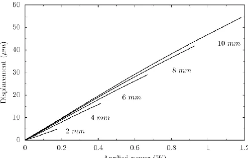
The length of the actuator beam is one of the parameters that determine the maximum tip displacement. Fig. 10 shows that as the injected power is increased the displacement generated also increases linearly, but with different slopes for different beam lengths. For example, a beam with an initial rake angle (inclination angle) of 3° a width of 20 μm and a 6 mm full length, the movable tip (Fig. 6) would experience a displacement of 20 μm for an injected power of 450 mW, assuming no external opposing force (i.e. unloaded displacement).
Fig. 10. Actuator tip displacement versus power for different beam full lengths with an initial rake angle of 3°.
It was found that the effect of changing the beam width was not significant on the microactuator displacement. The value selected for this design parameter is linked to the fabrication capabilities. For the fabrication process used, a 20 μm width beam could be released with confidence using the undercut provided during the oxide etch.
The term 0 represents the initial rake angle of the beam (see Fig. 6). This is a design variable, and therefore it is of interest to investigate the effect of changing its value. Fig. 11 shows the impact of the initial rake angle on the final actuator tip displacement. The results shown were calculated with 50 mA excitation, and shows that the actuator tip displacement will decrease as the angle increases. Fig. 11 indicates that there is no significant displacement for angles beyond 5-7°.
Fig. 11. Effect of the initial rake angle on the chevron microactuator displacement, applied current was 50 mA.
[image:8.612.48.300.110.271.2]The analysis also revealed that beyond a 6 mm length, the displacement/power stabilizes, meaning that a longer device would not improve the displacement/power ratio for a given 0. This trend is seen in Fig. 12. Therefore, a 6 mm long beam (half length L1 = 3 mm) was selected for the experimental device to deliver a suitable displacement/power characteristic.
Fig. 12. Actuator displacement per Watt electrical power for different beam lengths and rake angles.
C. Force analysis results (loaded state)
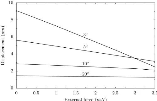
[image:8.612.316.566.170.334.2] [image:8.612.313.566.452.612.2] [image:8.612.49.298.470.629.2]angles. The reciprocal of the gradient of the curves in Fig. 13 is equal to the stiffness ka of the actuator. The values of ka
calculated for different rake angles will be used later in this section. It can be seen that the smaller rake angles have lower stiffness.
Fig. 13. Displacement versus opposing force for a beam length of 6 mm, width of 20μm and injected current of 100 mA (201 mW).
In our particular VOA format, the displacement of the actuator will be dependent on the external opposing force due to the combined stiffness of the optical fiber and the silicon restoring spring (kfs), as well as the inherent stiffness of the
actuator itself. The loaded displacement (δloaded) is related to
the unloaded displacement (δunloaded) through equation (25).
𝛿𝑙𝑜𝑎𝑑𝑒𝑑 = 𝛿𝑢𝑛𝑙𝑜𝑎𝑑𝑒𝑑[𝑘 𝑘𝑎
𝑎+𝑘𝑓𝑠] (25)
Table II shows the values of the stiffness of an actuator of length 6 mm for different values of rake angle, where stiffness is equal to the inverse of the slope of the graphs of Fig. 13.
TABLEII
STIFFNESS OF A 6MM BEAM AT EACH RAKE ANGLE FROM FIG.13 Angle (degs) ka (N/m)
3 531 5 1407 10 4842
From beam theory, it can be shown that the value of kfs is
𝑘𝑓𝑠= 3 (𝐸𝐿𝑠𝑖𝐼𝑟𝑠
𝑟𝑠 3 +
𝐸𝑔𝑙𝑎𝑠𝑠𝐼𝑖𝑓
𝐿𝑖𝑓3 ) (26)
where the equation parameters are given in Table III. Using equation (26) and Table III results in a value for kfs of 94.4
N/m. Next, by using equation (25) and Fig. 12 (for a 6mm beam length) we can calculate a figure of merit, defined as the displacement per Watt for the loaded case (due to fiber and restoring spring), for each of the initial rake angles shown.
TABLEIII
NOMENCLATURE AND VALUES FOR EQUATION (26)
Variable Symbol Value
Youngs modulus of Silicon Esi 167 GPa
Length of restoring spring Lrs 810 μm
Youngs modulus of optical fiber Eglass 71.7 GPa
Length of optical fiber Lif 3880 μm
Moment of inertia of restoring spring
Irs 𝑇𝑠𝑖𝑊𝑟𝑠3
12
Moment of inertia of fiber Iif 𝜋𝐷𝑖𝑓4
64
Width of silicon restoring spring Wrs 20 μm
Thickness of restoring spring Tsi 80 μm
Diameter of optical fiber Dif 125 μm
Of these angles, Table IV shows that the highest figure of merit i.e. the highest loaded displacement per Watt is obtained using a 3° rake angle, hence this value of rake angle is chosen for our microfabricated VOA.
TABLEIV
DISPLACEMENT PER WATT FOR 6MM LOADED ACTUATOR
Rake Angle (degrees)
𝒌𝒂
𝒌𝒂+ 𝒌𝒇𝒔
Unloaded Displacement (μm/W) from Fig.12
Loaded Displacement (μm/W) multiply column 2 by column 3) 3 0.849 44 37.4 5 0.937 26.5 24.8 10 0.981 14 13.7
[image:9.612.324.526.72.239.2]Fig. 14 shows the displacement versus opposing force curves for different input currents ranging from 30 mA to 140 mA obtained from the analysis. The device had 6 mm long beams, with an initial rake angle 0 of 3° and a width of 20 μm. As expected, higher input currents provide larger initial displacements (external force = 0). The devices that were built and tested have more than a single beam, so the total forces that can be generated are higher. The force generated with a multi beam chevron actuator increases with the number of beams [42].
[image:9.612.48.298.122.283.2] [image:9.612.317.560.556.711.2]The displacement between the two optical fibers is converted to the theoretical optical attenuation between the two single-mode fibers with misaligned axis and was calculated using the equation (27) derived by Jeunhomme [43] where TR is the optical transmission, x is the offset distance
from the maximum fiber alignment and w0 is the mode field radius of the single mode fiber used.
2
0 max 4.34
)
(
w x T
dB
TR R (27)
The attenuation in optical transmission (shown in Fig. 15) was calculated assuming initially zero attenuation (TRmax = 0) and a
[image:10.612.48.298.252.408.2]mode field radius of the optical fibers used equal to 5.4 µm.
Fig. 15 Displacement generated by the chevron microactuator (initial angle of 3°, width of 20 μm, and length of 6 mm) and the associated attenuation of optical power between two fibers mounted in the fiber channel.
In summary, we have analyzed electrothermal chevron microactuators and we have concluded that a beam full length of 6 mm, width of 20μm, together with a rake angle of 3° will provide a suitable force/displacement performance for an experimental device.
V. MICROACTUATOR EXPERIMENTAL CHARACTERIZATION
The previous section of this paper described the electro-thermal-mechanical modeling of the chevron microactuator and applied these results to determine the theoretical attenuation versus power response of our VOA design. An experimental MEMS device whose chevron microactuator design was based on the above results has been designed and fabricated, and tests were subsequently undertaken. The description of the experimental test process and results obtained are presented in this section, which describes the steady state behavior of the devices, analyzing the current-voltage characteristics, temperature distribution and mechanical displacements.
The beam design of the chevron microactuators selected by modeling had half-lengths of 3 mm, an initial 0 of 3°, width
of 20 μm, and thickness of 80 μm. Microactuators fabricated with different number of parallel beams (2, 4, 6, 8 and 10 beams on each side) were tested. All the beam anchors were connected to pads as shown in Fig. 1a. These anchors were also used to connect the device electrically to external equipment. The pads were large enough to use standard probes and make the electrical connections to the power supply (Farnell LT30-2). Two multimeters (Vellem DVM98) were used to measure the voltage and the current through the MEMS microactuator. An on-screen cursor based measurement system (IQ115 Cortex Controllers Ltd.) attached to a microscope with a digital camera (Nikon Coolpix 4500) was used to measure the mechanical displacements.
The position accuracy was determined by the resolution of the optical image transferred to the on-screen measurement system captured by the microscope (×25) with the Nikon Coolpix 4500 digital camera (×4 optical zoom), and the resolution of the on-screen measurement system (500 × 500 on-screen digital positions). The positioning resolution in the experimental setup was estimated to be 0.2 μm.
Current-voltage (I-V) curves of the microactuators with different number of beams were obtained by applying a voltage and recording the electrical current through the circuit. Fig. 16 shows the I-V measurement results. As expected, for an increased number of beams the resistance of the microactuator reduced in a parallel resistance summation manner. Hence, the current in the circuit increased for each arm added to the actuator. The error bars are based on the standard error calculated with respect to the modeling results.
Fig. 16. Experimentally measured current and voltage results from chevron microactuators with different number of beams.
[image:10.612.316.566.412.570.2](1+T)). Thus, the current starts to become non-linear. This effect was also captured in the models developed in Section III and presented in Fig. 18. The currents measured in tests shown in Fig. 18 were normalized (divided by the number of beam pairs) to a one beam device to directly compare them to values obtained from the modeling. The error bars are based on the standard error calculated with respect to the modeling results.
[image:11.612.49.298.147.300.2]Fig. 17. Resistivity of electrical path versus power on chevron type microactuators.
Fig. 18. Adapted experimental I-V curves versus model results.
The temperature of the microactuator was recorded at different applied voltages. This was done using K-type 50 μm tip diameter bare wire thermocouples Model CHAL-001 from Omega Engineering Limited and a digital thermometer Omega HH11. For each applied voltage the current through the microactuator was recorded and the thermocouple was positioned on the beam at specified locations to the half-way point of the actuator (at the following positions: 0 μm, 400 μm, 800 μm, 1200 μm, 1600 μm, 1800 μm, 2200 μm, 2600 μm and 3000 μm) using precision positioning stages and the IQ115 on-screen measurement system previously described. At each location the temperature was recorded. The process was repeated for higher voltage levels.
The measured temperatures and the analytical results are shown in Fig. 19 for a device with 10 beams. The triangles represent experimental measurement points. The temperature measurements on the micromechanical beams of 20µm width were undertaken using available bare wire K-type
thermocouples having 50 µm tips. The difference between experimental and modeling values is most likely due to the mismatch in size between the temperature probe tip and the beam being measured. Measurement errors of similar magnitude have been reported in [46] where the same type of temperature measuring probes were used. Qualitatively, the measurements show a general trend matching with that predicted by the modeling.
It can be seen from both the analytical and experimental results that the temperature at the center is slightly lower than that of the adjacent regions. This is due to the shuttle which is formed from the cross-connecting beams at the center of each chevron beam actuator. The chevron beams are modeled to be identical to each other, therefore no net electric current flows through the cross-connecting beams. However, heat flows into the shuttle from the center of the chevron beams, thereby lowering the temperature.
Fig. 19. Electrothermal analytical versus experimental test results.
[image:11.612.314.568.263.436.2] [image:11.612.48.300.336.492.2]Fig. 20. Experimental results for displacement versus applied electrical power (unloaded).
Fig. 21. Beam displacement versus normalized (per beam) power, analytical models versus test result.
VI. OPTICAL CHARACTERIZATION OF VARIABLE OPTICAL
ATTENUATOR
Using the microactuator investigated above and the latching system described in Section II within the set-up of Fig.1b, a fiber-to-fiber variable optical attenuator was demonstrated. Broadband light from an erbium doped fiber amplifier passed through the attenuator and the transmitted power recorded using an optical spectrum analyzer. The displacement measurement system measured the optical fiber position. Initially the two optical fibers were offset by 5 μm to ensure the transmission level passed through a maximum power as the fiber moved with electrical power applied to the microactuator.
The separate electrical circuit used to activate the latching mechanism (Fig. 3) did not work as expected. Due to inherent friction in the final fabricated MEMS device, the latching mechanism did not operate as well as the simulation predicted and a higher operating voltage (4.0 V as opposed to 3.4 V) was needed in the practical device to release the latches, resulting in temperatures above 1000°C at certain points within the gold coated mechanical latches. Hence the latch actuators experienced thermal damage from the latch current resulting in blistering and separation of parts of the gold layer
due to reaching a temperature very close to melting point of gold. Nevertheless, the mechanical part of the latching mechanism was fully functional and achieved the stable optical attenuation steps via 0.5 µm incremental steps of the fiber. Moreover, the problem of thermal damage to the conducting layer of the latching mechanism may be overcome by using an alternative higher melting point metal such as tungsten. Gold (resistivity 37.6 nΩ-m) has a melting point of 1060°C, whereas tungsten (resistivity 56.5 nΩ-m) has a higher melting point of 3420°C.
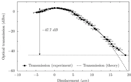
For each latched position an optical transmission and a fiber displacement measurement was recorded. Fig. 22 shows the optical transmission between the fibers measured at each latched position, together with the theoretical transmission calculated using the equation (27).
Fig. 22. Optical transmission for different latched positions, theoretically estimated light transmission and optical resolution for fiber coupling. The RMS value of the difference between the theoretical and the experimental values was 0.16 dB.
The electrical power required by the actuator to displace the movable fiber by 23 μm (5 μm from the initial offset to full alignment plus a further 18 μm to achieve the attenuation of 47.7 dB) was measured to be 6.2 W for a 10 beam device. Our actuator array was designed with ten chevron beams to provide an adequate “safety margin” because of the unknown Vernier latching mechanism friction in this new design. However, the theoretical model (Fig. 15) has shown that as few as one chevron beam can generate sufficient force to displace the particular fiber/spring combination used in our VOA design. Therefore, future designs of this VOA platform will aim to minimize the number of beams used. In addition, this should also lead to a significant reduction in the electrical power consumption.
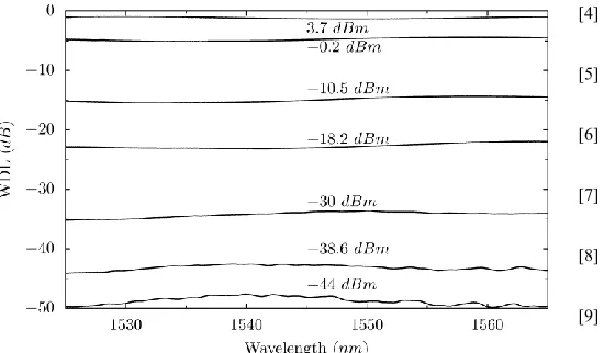
[image:12.612.312.566.235.394.2] [image:12.612.48.298.247.406.2]Fig. 23. Optical wavelength dependent transmission along the C-Band for the different latched positions. These results were obtained by referencing against an uninterrupted fiber transmitting 4.77 dBm.
VII. CONCLUSION
The electro-thermo-mechanical modeling of a chevron type microactuator was undertaken and performance results for most design parameters have been presented. Single-crystal silicon microactuators were fabricated for experimental evaluation and results were found to be in agreement with the predictions of the modeling. The microactuators were configured to form a VOA that used fiber-to-fiber coupling losses as the means of attenuating the optical signal in the fiber. A Vernier latching mechanism incorporated into the microactuator allowed incremental steps within the full translation range to be fixed in position and demonstrated an experimental 0.5 μm step resolution. Latching of the attenuation level was demonstrated with no electrical energy input required to hold the attenuation state. In addition, the attenuation is based on fiber-to-fiber displacement and not on a shutter mechanism and therefore there are no moving parts between the end-faces of the optical fibers that could vibrate and modulate the optical signal. Over the full translation range, the attenuation of the optical signal was measured at over 47 dB, whilst the wavelength dependent loss over the C-band was 1.4 dB at 40 dB attenuation. With an insertion loss of around 1 dB and a transition time of 1.7 ms, this device can find application in an optical network for optical power management.
ACKNOWLEDGMENT
The authors would like to convey their thanks to Professor Richard Syms, Imperial College London, for helpful discussions during the performance of this research.
REFERENCES
[1] S. Cohen, “Novel VOAs provide more speed and utility”, Laser Focus
World, vol. 36, pp. 139-146, Nov. 2000.
[2] J. E. Ford, J. A. Walker, D. S. Greywall, and K. W. Goossen, “Micromechanical fiber-optic attenuator with 3 µs response,” J.
Lightwave Technol., vol. 16, no. 9, pp. 1663-1670, 1998.
[3] C. Lee and J. A. Yeh, “Development and evolution of MOEMS technology in variable optical attenuators,” J. Micro/Nanolith. MEMS
MOEMS, vol. 7, no. 2, pp. 021003-1 - 021003-16, 2008.
[4] C. Marxer, P. Griss, and N. F. de Rooij, “A variable optical attenuator based on silicon micromechanics,” IEEE Photon. Technol. Lett., vol. 11, no. 2, pp. 233-235, 1999.
[5] R. R. A. Syms, H. Zou, J. Stagg, and D. F. Moore, “Multistate latching MEMS variable optical attenuator,” IEEE Photon. Technol. Lett., vol. 16, no. 1, pp. 191-193, 2004.
[6] J. C. Chiou and W. T. Lin, “Variable optical attenuator using a thermal actuator array with dual shutters,” Opt. Commun., vol. 237, no. 4-6, pp. 341-350, 2004.
[7] L. Li and D. Uttamchandani, “Design and evaluation of a MEMS optical chopper for fiber optic applications,” IEE P-Sci. Meas. Tech., vol. 151, no. 2, pp. 77-84, 2004.
[8] R. R. A. Syms, H Zou, J Stagg and H Veladi, “Sliding-blade MEMS iris and variable optical attenuator,” J. Micromech. Microeng., vol. 14, pp.1700-1710, 2004.
[9] L. J. Li, J. Zawadzka and D. Uttamchandani, “Integrated self-assembling and holding technique applied to a 3-D MEMS variable optical attenuator,” J. Microelectromech. Syst., vol 13, no. 1, pp. 83-90, 2004. [10] C. Lee, “Variable optical attenuator using planar light attenuation
scheme based on rotational and translational misalignment,” Microsyst. Technol., vol. 13, no. 1, pp. 41-48, 2007.
[11] T. S. Lim, C. H. Ji, C. H. Oh, H. Kwon, Y. Yee, and J. U. Bu, “Electrostatic MEMS variable optical attenuator with rotating folded micromirror,” IEEE J. Sel. Top. Quant., vol. 10, no. 3, pp. 558-562, 2004.
[12] H. Cai, X. M. Zhang, C. Lu, A. Q. Liu, and E. H. Khoo, “Linear MEMS variable optical attenuator using reflective elliptical mirror,” IEEE Photon. Technol. Lett., vol. 17, no. 2, pp. 402-404, 2005.
[13] X. M. Zhang, A. Q. Liu, H. Cai, A. B. Yu, and C. Lu, “Retro-axial VOA using parabolic mirror pair,” IEEE Photon. Technol. Lett., vol. 19, no. 9-12, pp. 692-694, 2007.
[14] K. H. Koh, C. Lee and T. K.obayashi, “A piezoelectric driven 3-D MEMS VOA using attenuation mechanism with combination of rotational and translational effects,” J. Microelectromech. Syst., vol. 19, no. 6, pp. 1370-1379, 2010.
[15] K. H. Koh, Y. Qian and C. Lee, “Design and characterization of a 3D MEMS VOA driven by hybrid electromagnetic and electrothermal actuation mechanisms,” J. Micromech. Microeng., vol. 22, no. 10, pp. 1-13, 2012.
[16] X. Dai, X. Zhao, G. Ding, and B. Cai, “Micromachined electromagnetic variable optical attenuator for optical power equalization”, J. Microlith.,
Microfab. Microsyst., vol. 4, no. 4, pp. 041304-1 – 041304-5, 2005.
[17] M. Hoffmann and E. Voges, “Bulk silicon micromachining for MEMS in optical communication systems”, J. Micromech. Microeng., vol. 12, no. 4, pp. 349-360, 2002.
[18] C. Lee, “A MEMS VOA using electrothermal actuators,” J. Lightwave Technol., vol. 25, no. 2, pp. 490-498, 2007.
[19] K. R. Cochran, L. Fan, and D. L. DeVoe, “High-power optical microswitch based on direct fiber actuation,” Sensor. Actuat. A-Phys., vol. 119, no. 2, pp. 512-519, 2005.
[20] R. R. A. Syms, H. Zou, J. Yao, D. Uttamchandani, and J. Stagg, “Scalable electrothermal MEMS actuator for optical fiber alignment,” J.
Micromech. Microeng., vol. 14, no. 12, pp. 1633-1639, 2004.
[21] I. H. Hwang, Y. S. Shim, and J. H. Lee, “Modeling and experimental characterization of the chevron-type bi-stable microactuator,” J.
Micromech. Microeng., vol. 13, no. 6, pp. 948-954, 2003.
[22] W. C. Chen, C. Lee, C. Y. Wu, and W. L. Fang, “A new latched 2 x 2 optical switch using bi-directional movable electrothermal H-beam actuators,” Sensor. Actuat. A-Phys., vol. 123-24, pp. 563-569, 2005. [23] Z. L. Huang and J. Shen, “Latching micromagnetic optical switch,” J.
Microelectromech. Syst., vol. 15, no. 1, pp. 16-23, 2006.
[24] S. Oak, S. Rawool, G. Sivakumar, E.J. Hendrikse, Jr., D. Buscarello, and T. Dallas, “Development and Testing of a Multilevel Chevron Actuator-Based Positioning System, ” J. Microelectromech. Syst., vol. 20, no.64, pp. 1298-1309, 2011.
[25] S. Anand, J. Sutanto, M. S. Baker, M. Okandan, and J. Muthuswamy, “Electrothermal microactuators with Peg drive improve performance for brain impact applications,” J. Microelectromech. Syst., vol. 21, no. 5, pp. 1172-1186, 2012.
[26] Y. B. Gianchandani and K. Najafi, “Bent-beam strain sensors,” J. Microelectromech. Syst., vol. 5, no. 1, pp. 52-58, 1996.
[27] R. R. A. Syms, H. Zou, and J. Stagg, “Micro-opto-electro-mechanical systems alignment stages with Vernier latch mechanisms,” J. Opt.
[28] A. Unamuno and D. Uttamchandani, “MEMS variable optical attenuator with Vernier latching mechanism,” IEEE Photon. Technol. Lett., vol. 18, pp. 88-90, 2006.
[29] H. Guckel, J. Klein, T. Christensen, K. Skrobis, M. Laudon and E. G. Lovell, “Thermo-magnetic metal flexure actuators” presented at 5th Technical Digest, IEEE Solid-State Sensor and Actuator Workshop
(Hilton Head Island, SC, USA, 22–25 June 1992) pp 73.
[30] D. J. Bell, T. J. Lu, N. A. Fleck, and S. M. Spearing, “MEMS actuators and sensors: observations on their performance and selection for purpose,” J. Micromech. Microeng., vol. 15, no. 7, pp. S153-S164, 2005. [31] Y. J. Lai, J. McDonald, M. Kujath, and T. Hubbard, “Force, deflection and power measurements of toggled microthermal actuators,” J.
Micromech. Microeng., vol. 14, no. 1, pp. 49-56, 2004.
[32] A. M. H. Kwan, S. Song, X. Lu, L. Lu, Y-K. Teh, Y-F. Teh, E. W. C. Chong, Y. Gao, W. Hau, F. Zeng, M. Wong, C. Huang, A. Taniyama, Y. Makino, S. Nishino, T. Tsuchiya, and O. Tabata, “Improved designs for an electrothermal in-plane microactuator,” J. Microelectromech. Syst., vol. 21, no. 3, pp. 586-595, 2012.
[33] A. Cao, J. B. Kim, and L. W. Lin, “Bi-directional electrothermal electromagnetic actuators,” J. Micromech. Microeng., vol. 17, no. 5, pp. 975-982, 2007.
[34] R. Hickey, D. Sameoto, T. Hubbard and M. Kujath, “Time and frequency response of two-arm micromachined thermal actuators,” J.
Micromech. Microeng., vol. 13, no.1, pp. 40-46, 2003.
[35] R. S. Chen, C. Kung, and G. B. Lee, “Analysis of the optimal dimension on the electrothermal microactuator,” J. Micromech. Microeng., vol. 12, no. 3, pp. 291-296, 2002.
[36] N. D. Mankame and G. K. Ananthasuresh, “Comprehensive thermal modeling and characterization of an electro-thermal-compliant microactuator,” J. Micromech. Microeng., vol. 11, no. 5, pp. 452-462, 2001.
[37] Y. Zhang, Q. Huang, R. Li, and W. Li, “Macro-modeling for polysilicon cascaded bent beam electrothermal microactuators,” Sensor. Actuat. A-Phys., vol. 128, no. 1, pp. 165-175, 2006.
[38] E. T. Enikov, S. S. Kedar, and K. V. Lazarov, “Analytical model for analysis and design of V-shaped thermal microactuators,” J.
Microelectromech. Syst., vol. 14, no. 4, pp. 788-798, 2005.
[39] L. W. Lin and M. Chiao, “Electrothermal responses of lineshape microstructures,” Sensor. Actuat. A-Phys., vol. 55, no. 1, pp. 35-41, 1996.
[40] S. Krenk, Mechanics and Analysis of Beams, Columns and Cables. Springer-Verlag, 2001.
[41] M. A. Hopcroft, W. D. Nix, and T. W. Kenny, “What is the Young’s modulus of silicon?,”J. Microelectromech. Syst., vol. 19, no. 2, pp. 229-238, 2010.
[42] J. Qiu, J. H. Lang, and A. H. Slocum, “A curved-beam bistable mechanism,” J. Microelectromech. Syst., vol. 13, no. 2, pp. 137-146, 2004.
[43] L. B. Jeunhomme, Single-mode fiber optics. Principles and applications, 2nd ed., New York: Marcel Dekker Inc., 1990, pp. 96-123.
[44] A Cowen, G Hames, D Monk, S Wilcenski and B Hardy “SOIMUMPs design handbook (revision 8), MEMSCAP Inc.” [Accessed March 2013]. [online:
http://www.memscap.com/__data/assets/pdf_file/0019/1774 /SOIMUMPs.dr.v8.0.pdf].
[45] R. B. Roberts, “Thermal-expansion reference data - silicon 300-850-K,”
J. Phys. D Appl. Phys., vol. 14, no. 10, pp. L163-L166, 1981.
[46] C. Jenkins, G. Brown, W .Johnstone and D. Uttamchandani, “MEMS Actuated Small Scale Retroreflectors for Free Space Optical Communications,” Journal of Optics A: Pure and Applied Optics, vol. 8, pp S384-S390.
Anartz Unamuno received the Ph.D. degree from the University of Strathclyde, Glasgow, UK for research on hybrid optical MEMS. In 2006 he joined Cavendish Kinetics B.V. to work on the design and modeling of MEMS components, including MEMS based non-volatile memory and RF-MEMS variable capacitors. He is currently with the Fraunhofer IPMS where he is applying MEMS technologies to engineering applications.
Robert Blue received the Ph.D. degree in Optical Electronics from the University of Strathclyde, Glasgow, U.K., in 1996. He is currently at the Centre for Microsystems and Photonics, University of Strathclyde. His research interests include MEMS-based wavelength selective devices using
whispering gallery modes, and the development of MEMS explosive sensors incorporating novel nitro-sensitive polymers.