Abstract: This paper presents design of Transformer Feed-Back (TFB) Common Source (CS) Low Noise Amplifier (LNA)and implemented in 65 nm CMOS process parameters for operation at 60 GHz. The LNA is composed of four cascaded CS stages by utilizing gate-source TFB at the input side for input impedance matching to reduce the noise figure. The drain-source TFB is applied to the remaining stages for gain improvement, interstage and output matching. The designed LNA is simulated with Advanced Design System (ADS) and verified its functionality with respect to Noise Figure (NF), Gain, Linearity, Power dissipation and Stability. Simulated results of the proposed LNA show 23.91 dB of gain, 5.58 dB of NF and -7 dBm of IIP3 to accomplish linearity. The Figure of Merit (FoM) describes as a component of the linearity, gain and NF is 27 while drawing 15 mA from a 1.0 V supply.
Keywords: 60 GHz, ADS, Transformer Feedback, Low Noise Amplifier, High Gain, Low NF
I. INTRODUCTION
Radio Frequency (RF) transceivers market demands communication links of higher data rate in the Industrial Scientific Medical (ISM) band at 60 GHz. RF systems operating in 60 GHz frequencies require receivers with a low Noise Figure (NF) and flat band response. The low NF, high gain, acceptable bandwidth, Figure of Merit (FoM), Stability and operation at low voltage are vital properties of LNAs that form the first subsystem in RF receiver. One of the design challenges in RF systems is selection of semiconductor technology. Microwave Integrated Circuits (MMICs) have been composed using III-V semiconductor technologies, such as Gallium Arsenide (GaAs) or Indium Phosphide [InP] reported in [1-3]. An expanding number of building blocks at 60 GHz and systems have been recently reported in SiGiBiCMOS [4-8] and CMOS technologies [9]. CMOS technology promises higher levels of integration, reduced cost, size and powerconsumption (PDC). CMOS implementation also benefits from Moore’s Law [9], and CMOS performance is enhancingat regular intervals, expanding its usefulness into mm-wave frequencies [19]. SiGe Heterojunction Bipolar Transistor (HBT) technology offers maximum cut-off frequency (fT) [10]competitive with
Revised Manuscript Received on June 05, 2019
RajendraChikkanagouda, Research Scholar, Department of ECE, M. S. Engineering College, Bengaluru, India
Cyril Prasanna Raj P., Senior Member, IEEE, Dean (R & D), M. S. Engineering College, Bengaluru, India
GaAs, although GaAs still offers better integration of passives and better power-handling capability. Considering the discussions reported in literature studies CMOS technology for LNA design is preferred. Millimeter-wave LNA’s design in CMOS causes numerous challenges due to passive component losses and the Miller capacitance. The studies on design of LNA’s using CMOS technology operating in the frequency range of 60 GHz are reported [12], [16-22], [25-28],[35]. A significant number of the earlier reported LNA’s matching networks are designed with Transmission Lines (TL) which occupies moderatelymore chip area even at mm-wave band.In contrast, more area-efficient design approach can be achieved with the help of inductors (spiral). In this work design of 60 GHz LNA circuit using CMOS technology based on cascaded Common Source (CS) topology with Transformer Feed-Back (TFB) to achieve flat and broad response along with Gate-Source (G-S) and Drain-Source (D-S) circuitry for design of 4-stage CS LNA is presented. Area optimization of LNA circuitry is achieved by adopting TFB technique [9], [11], [14], [17]. Miller effect can be reduced using G-D capacitance neutralization [9], [18], [23]. Background theory, process technology and existing LNA designs are reported in section II. Designing a LNA for mm-wave applications and its simulation setup are presented in section III and section IV. Discussion on results is reported in section V. Section VI provides conclusion.
II. BACKGROUNDTHEORY
A. Process Technology
In this section a detailed discussion on different process technologies and various CMOS topologies for LNA design that have been considered as industry standard is reviewed. The performance of front-end units can be upgraded through Gallium-Nitride (GaN) [3] technology over the past GaAs semiconductors [2] due to its wider bandgap, greater electron mobility and good thermal conductivity which results better linearity, superior power density and low noise over a broader operating bandwidth [3].Silicon-Germanium (SiGe) technology may well start to interfere with mm-wave, however, since the transition (fT) and maximum oscillation (fmax) frequencies of the most developed bipolar transistors exceed 200 GHz [4]. SiGe guarantees high levels of integration, which should lower cost and power dissipations.
High Gain Low NF Stable Transformer
Feedback Common Source LNA Design for 60
GHz Applications
CMOS technology is exclusively responsive for its ability of integration with Intermediate Frequency (IF) and DSP functions (base-band) empowering trueSoC(Systems on Chip) [13].The Current-Voltage (I-V) characteristics become linear in sub-micron CMOS technology and hence there is an enhancement in the performance parameters such as NF, fT, fmax,gm (transconductance). Be that as it may, the potential inclinations are joined by disadvantages, such as reduced breakdown voltages, subsequently decreased linearity and scaling of the metal back-end.
There are several important LNA topologies such as the Common Gate (CG), CS, Cascode, Current Reuse (CR) and Distributed amplifier topology. The cascode topology is preferred for its robustness to process variation, better isolation and high gain. It has better linearity when compared to CS and CG configurations. The minimal stability and marginally higher NF are the main disadvantages of cascode [3, 6]. The output admittance of the cascode topology is quite low in comparison to the Common-Emitter (CE) topology because it has a low capacitive component [7]. The single-stage design is inefficient in meeting the expected design trade-offs. In this design, cascaded version of CS is preferred to maximize gain and minimize NF. For LNA design, various feedback techniques such as Resistive FeedBack (RFB), Series-series FeedBack (SFB), Shunt-Series FeedBack (SSFB) and TFB are used. Generally Cascode and CS topologies without CG feedback, cannot accomplish simultaneous noise and impedance matching. At the input of the SFB LNA, the pad capacitance adds the additional resonant circuit at mm-wave frequencies. Input impedance matching and noise impedance over an extended bandwidth turns out to be more hazardous. SSFB simultaneously compensates the transistor pad capacitance and the input capacitance over a wider bandwidth [14]. Reactive feedback [11] decreases the NF, balances the gain, and sets the terminal impedances within the recommended bandwidth. Negative feedback is an alternative method to limit the terminal impedances, isolation, gain and NF. For wideband amplification, negative feedback has various advantages including gain stability over PVT variations, reduced distortion, minimum noise and impedance matching [11]. As losses are reasonably small in the transformer windings, the TFB technique contributes reduced noise [18], [21]. The gate-drain capacitance in the Field-Effect Transistor (FET) is neutralized by using TFB technique [9]. These benefits come at the cost of chip area and design complexity [21], [27].
The transformer based topology is preferred for improving noise and matching networks. CR technique is also preferred to achieve for low power. To decrease the signal loss and undesired coupling from layout point of view the GCPW) (Grounded Co-Planar Waveguide) structure is utilized [17]. Compared with the two separate inductors (gate and source), the LNA design with transformer occupies less chip area and better quality factor. By using transformer based technique,the matching network insertion loss can be minimized and improves NF. TL and inductor (lumped) are the two basic components used to model the LNA circuit [15]. The TL offers a very much characterized Electro Magnetic (EM) condition that speeds up the structure at the cost of chip area.The smaller dimensions are offered by lumped inductor but is more exposedto coupling that
degrades the performance of the LNA. It requires standard EM simulations which leads to lengthy design cycle [15].
B. Existing LNA Designs
Literature review on different LNA designs with respect to process technologies, gate length and LNA topologies are discussed and summarized in the present section.
LNA circuits working in the V-band have been existing for several decades today. Bharatha Kumar et al., [8] have demonstrated 4 stage bidirectional LNA in 0.18µm SiGeBiCMOS process from (54 to 65) GHz by using transistor bias control and low-loss coplanar waveguide structures. The LNA exhibits 18.8 dB of gain, NF of 7.7 dB, P1dB of -18.5 dBm and consumes 19.9 mW of power. Po-Yu Chang et al., [21] have published four cascaded CS stage LNA in 90 nm CMOS operating at 60 GHz. The LNA achieves a peak gain of 12.5 dB and a 5.4 dB of minimum noise figure (NFmin).ThePDC of the LNA is 4.4 mW from a 1.0 V supply. Aili Wang et al. [27] developed three stage CS LNA in 65 nm LP CMOS process operating at 60 GHz. The circuit achieves a gain of 22 dB, NF of 5.5 dB and the IIP3 is -10.7 dBm operating at 61 GHz with a PDC of 26 mW from a 1.2 V supply. Mizutani et al., [29] have published an optimum interstage matching inductor of a cascode amplifier in 90 nm CMOS process. LNA achieved 25.6 dB gain with NF of 6 dB, P1dB -2.3 dBm and PDC of 26.9 mW. S11 is -12 dB and S22 is -4 dB.J.O. Plouchart et al., [30] have demonstrated 3-stage cascode LNA implemented in a 32 nm SOI CMOS technology operating at 60 GHz exhibits a peak gain of 21dB, an average 3.3 dB NF from (53 - 62) GHz and 18 mW of PDC. Di Sheng Siao [28] presented a variable gain amplifier (VGA) in standard RF 65 nm CMOS process operating from (57-66) GHz. The phase compensation is achieved by using the phase between current-steering and splitting-cascade topologies. The LNA achieve 21 dB of gain, input and output return losses are -6.5 dB and -5 dB, P1dB of -4 dBm, consumes 10.9 mW power and phase variation of less than 7 °. FanyiMeng et al., [31] reported a bidirectional LNA in 65 nm CMOS technology. The Rx mode features peak gain of 21.5 dB with gain greater than17 dB over (57-67) GHz, NF of 6.7 dB, S11 and S22 are -14 dB and -8 dB with PDC of 39.6 mW and FoM is 4.8. Kun-Yao Kao et al., [32] presented Variable Gain(VG) LNAwith 65 nm CMOS technology which supports 60 GHz band. The current-steering architecture provides variable gain functionality. The measured peak gain is 19.8 dB at 66 GHz, 4.3 dB of NFminat 60 GHz, and PDC is 28.8 mW. The return loss is greater than -10 dB. M. M. Fouad et al., [33] have demonstrated two stage LNA using TFB technique using TSMC 65 nm CMOS technology. The transformer is used to neutralize with Miller capacitance of the FET. The LNA achieves transducer gain (Gt) of 12.2 dB with NF of 4.27 dB and IIP3 is 5.6 dBm, while it consumes 30 mW from 1.2 V. Hiroyuki ShitaGuo et al., [34] proposed design of three stage TFB LNA in 65 nm CMOS technology with gain improvement and noise reduction simultaneously. LNA exhibits NFmin of 3.6 dB at 53.5 GHz and a highest power gain of 28.2 dB at 54 GHz, P1dB of 29.4 dBm and consumes 9.8 mW of power. SuryanarayananSubramaniam et al., [35] have been demonstrated design of two-stage CS LNA in 45 nm CMOS process technology and have shown the LNA operating at 60 GHz frequency. The LNA achieves gain of 17.2 dB, NF of 2.8
III. 60 GHZLNA DESIGN
The V-band LNA using 65 nm with TFB technique is depicted in Fig. 1. It employs four stage cascaded CS stages, with two different TFB configurations. For noise and input matching, Gate-Source (G-S) TFB is used at input stage. Drain-Source (D-S) TFB technique is used for achieving inter-stage and output matching with enhanced power gain from second to fourth stage.
In the current LNA design, identification of transistor geometries is carried out by considering design parameters reported in [21] and further tuning of the geometrical parameters as per desired specifications. Gain peaking which is a desired requirement is achieved by introducing the inductor at the drain of first stage, which also performs inter-stage matching. PDC is reduced by minimizing parasitic capacitances and accordingly the transistor geometries are identified for M2, M3 and M4. The corresponding specifications of the design are operating frequency between (57 – 65) GHz, NF less than 6 dB, gain greater than 15 dB, linearity and stability within the operating range. The LNA is modeled and parameters required to identify LNA perfomance are computed by using 65 nm Berkeley Short-channel IGFET Model (BSIM4) PTM model [35].
Vin
Vout Vdd
Vg Vg
Ld
L1 L2
L4
L3 L5
L6
L7 L8
Vg
Cin Cout
CC1 CC2 CC3
RG1 RG2 RG3
M1 M2 M3 M4
[image:3.595.53.286.350.495.2]Lout
Fig.1 Circuit schematic of the proposed 60 GHz TFB LNA
In LNA design matching network of the input side plays a vital role as it greatly influences the LNA performance by gain and NF. Source degeneration is generally used to attain ideal impedances for gain (Zin, opt) and NF (ZN, opt), that eases the trade-off between parameters such as gain and NF.
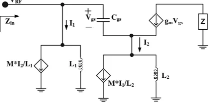
Z
Zin
M*I2/L1
M*I1/L2
L1
L2
Cgs
Vgs g
mVgs
I1
I2
VRF
Fig. 2 First stage SSM (Small Signal Equivalent) circuit The TFB technique used in the input stage of the LNA design not only to match the impedances but also extends the bandwidth operation [21]. The input impedance ( of
the LNA is calculated by using the small-signal equivalent model of the first stage as shown in Fig. 2, which is in Eq. (1) and Eq. (2).
(1)
(2)
The transformer coupling factor is k that satisfies
,
where M, n and gm are the mutual inductance, turns ratio and input transistor transconductance, the capacitance of gate to source is Cgs, L1is the primary inductance and L2 is the secondary inductance. The input impedances (real, imaginary) are given by Eq. (3)and
(3)
The proportion of L2/L1 could be sketched to maximize gm from smallervalue while the L1, L2 and their coupling are modelled to resonant with the input parasitic capacitance.
IV. LNADESIGNPROCEDURE
In this section discussions on reverse isolation technique such as unilateralization and neutralization is presented. Discussion on designing LNA to meet parameters like gain, NF, group delay is explained.
A. LNA Unilateralization and Neutralization
The effect of Cgd cannot be neglected on performance of transistors with increase in operating frequency. Cgd adds a (non-inverting) signal path which reduces reverse isolation as well as amplifier forward gain and also decreases (cut-off frequency) of the device [9] shown in Eq. (4).
(4)
The impact offt on the input capacitance is multiplied by the Miller effect in a CS configuration shown in Eq. (5).
(5)
Cgddegrades amplifier performance to find alternative ways to reduce Cgdeffects. Circuits that decrease the impact of Cgd are generally divided in to two groups: Unilateralization and Neutralization. Unilateralization decreases reverse signal flowand neutralization removes signal flow through Cgd by including additional paths. This surges S21 and S12 for a given PDC, but this does not scale down the impact of Cgd on the
input capacitance. Two examples of common
[image:3.595.66.278.573.678.2]stability and simpler matching network two stage design is preferred, Neutralisation can be divided into differential, inductor-tuned and TFB techniques. The neutralizing capacitor CN is used to remove the signal flow through Cgd in differential neutralization technique [8]. If CN >Cgd, the differential pair drain voltages are phase shifted by 180°, the current flowing through CN and Cgdis equal in magnitude and opposite in phase, which concludes neutralization. CN also doubles the effective capacitance at the input and drain nodes by Cgd, which unfavourably affects bandwidth, gain and terminal impedances. Inductor-tuned technique uses an inductor to resonate with Cgd. For monolithic implementations, this technique is impractical because the inductance value is too high to be integrated.
TFB technique is the third approach used for neutralization, which proposes magnetic coupling between drain and source inductors of a CS transistor [9]. Through the transformer, feeding back a portion of the output signal helps to eliminate the feedback from output to input through Cgd and neutralize the amplifier. The mutual inductance and turns ratio are derived by solving equations reported in [21].
B. Selection of Transformer parameters
Transformer turns ratio and coupling factor are the important parameters to achieve Cgdneutralization. The ratio of coupling factor (k) and transformer turns ratio (n) should be equal to the negative sign of Cgsand Cgdproportion. Turns ratio of transformer should be high to maximize the gain and the value of k lies between -1 to +1 [18]. The mutual inductance of first to fourth stage are found to be 9.64 pH, 8.57 pH, 9.62 pH and 9.90 pH and turns ratio of the transformer is found to be 2.0 to 2.4.
C. Noise Figure
The noise factor can be expressed in Eq. (6).
(6)
Where γ represents channel noise parameter [24]. The noise factor can be simplified under input-matching condition, expressed in Eq. (7).
(7)
NF can be limited by expanding n as it is observed from equation (7), F is independent of frequency assuming γ is to be constant. The input matching network comprises of gate inductance (Lg) and source inductance (Ls) as TFB and input capacitance (CIN) is designed to minimize the noise. For better input matching higher value of gm is preferred, but this impacts on transistor size or PDC. Additionally, the transformer quality factor and coefficient of coupling should be considered as unity.
The G-S and D-S TFB topologies are reported in [21] as G-S and D-S is used in first and subsequent stages respectively. The relationship between Cgs, Cgd, n and kcan be derived as [9], [23]
(8)
Meeting the requirements of Eq. (8), negative feedback offset and effects of Millers capacitance are reduced to achieve better gain. In practical design, Cgd/Cgscan be approximated from the transistor geometries and k is moderately small range (0.110–0.125).
D. Group Delay Analysis
The gain flatness and Group Delay (GD) are important factors for wideband amplifiers used to figure out the phase nonlinearity of amplifiers. In time domain signals, it is required to maintain minimum GD variationsto get non distortion amplification [30], [37]. The GD is expressed as the ratio of derivative of transfer function phase and angular frequency (ω), given by Eq. (9)
(9)
Where is the phase of the transfer function which is a function of angular frequency, ω.In order to reduce the GD variations, firstly, make the source and load impedance equivalent to the TL characteristic impedance. Secondly, make the signal path as short as possible in order to reduce the intrinsic transit time, which has a direct relationship with the magnitude of group delay variation and using differential transmission line instead of single-ended one is also helpful to minimize the group delay variation.
V. RESULTSANDDISCUSSIONS
LNA design carried out in previous section is modelled using schematic capture in ADS environment. ADS is well-known software for designing and optimizing microwave and RF circuits. BSIM4 technology and model files have been downloaded from predictive technology forum [41] and its parameters are brought into ADS for LNA design. The LNA design performance parameter’s results such as gain, NF, IIP3, P1dB, group delay and gain ripple have been obtained by performing simulation for the proposed LNA design which are shown in Fig. 3 to Fig. 8 with 65 nm technology. The TFB four stage LNA is analyzed for its gain response in the frequency range of (55-69) GHz.
A. Power Gain and Noise Figure Analysis
.
[image:5.595.322.523.58.214.2]Fig.3 Gain & NF of the proposed LNA
Fig. 4 S11 and S22 of the proposed LNA
The Figure 4 depicts input reflection coefficient (S11) less than -8 dB from 57 GHz and -10.37 dB at 63 GHz and output reflection coefficient (S22) is less than -7.6 dB and -9.88 dB at 63 GHz.
B. Phase Distortion Analysis
[image:5.595.73.256.59.211.2]The group delay of the proposed LNA is shown in Figure 5 varying from 30.75 pS to 23.54 pS between (50-70) GHz frequency of operation. The Group Delay of 30.75 pS is noted down at a frequency of 60 GHz. The group delay window (Δ) is 2.1 pS for (57-65) GHz frequency range.
Fig. 5 Group delay of the LNA
Fig. 6 Gain ripple of the LNA
In an amplifier design, the flatness is highly desired and can be achieved by controlling the ripple. The less difference between upper and lower limit of the amplitude will provide more flat band. The gain ripple of the proposed LNA is 2.67 dB between (57-69) GHz frequency of operation which is shown in Figure 6.
C. Linearity (P1dB and IIP3) Analysis
Linearity is one of the most crucial factor of performance for a wireless-system, directly related to inhibitors such as spectral regrowth in both single and multi-carrier systems. Amplifiers are nonlinear, active devices. At low-power levels, the output power follows input power. At higher power levels, the amplifier's power gain starts decreasing, it enters gain compression, further increases of input power the amplifier output power saturates and no additional power results at the output. Figure 7 shows gain compression point of the LNA, two compression points are compared with respect to input power. The compression points are linear (theoretical response) and Vout (actual response).The Voutfollows linear from -30 dBm to -20 dBm, 1-dB difference at -21 dBm and thereafter gain decreases with increase of input power.
[image:5.595.71.259.558.746.2]Intermodulation products of higher order present in the output spectrum due to nonlinearities impacts exhibit in a LNA circuit [38]. Among the different order intermodulation products, the most disturbing one is third order because its frequency is close to the fundamental product.
[image:5.595.322.522.577.717.2]Therefore, LNA nonlinearity is widely characterized by IIP3 [39]. Two harmonics are compared with the input power. The Vout [1,0] (fundamental) and Vout [-2,1]( 3rd order) meets at -7 dBm of the input power. The proposed cascode LNA for 65 nm IIP3 is -7 dBm, which is better than that of the existing LNAs.
Fig. 8 IIP3of the proposed LNA D. Stability Factor (K) and FoM Analysis
LNAs often exhibit undesired behaviour from certain input power value, which cannot be anticipated with a small-signal stability analysis. Spurious oscillations are commonly observed undesired phenomena [40]. Stability can be classified into two types. Conditional stability specifies to a network that is stable when the characteristic impedances of both input and output terminals are equal, but any mismatch on either source or load impedances that will cause it to oscillate. Unconditional stability indicates to a network that any possible impedance the amplifier should be stable. For LNA design, stability factor K is required to be satisfied as provided in Eq. (10). If the stability factor K is greater than one then LNA is said to be stable [36]. Figure 9 shows the stability factor K for the designed LNA whose value is greater than one for the entire frequency range.
> 1 (10)
Where S11 and S22 are the input and output reflection coefficients and S12 is reverse isolation. The value of Δ is calculated from S-parameters which is
. The FoMdepictsas acomponent of the Gain, NF, PDC and linearity is 27 [40].
[image:6.595.330.521.204.343.2]
Fig. 9LNA Stability Factor
E. Gain and NF versus Gate Voltage (VGS) Analysis
The analysis of gain and NF results with different gate to source voltages (VGS) is performed which is depicted in Figure 10. The VGS of the MOSFET is found to vary from 0.5 V to 1.0 V at 60 GHz operation. The maximum gain of the LNA is found to be 23.91 dB and NF of 5.59 dB at 60 GHz. The VGS of the MOSFET is found to vary from 0.7 V to 1.0 V to achieve S21 between 23.12 dB to 13.96 dB and NF between 6.04 dB to 8.65 dB. The gain decreases and NF increases by increasing the VGS. The maximum gain and minimum NF values are obtained at 0.6 V of VGS amplifier MOSFET.
[image:6.595.313.525.209.520.2]Fig. 10Gain and NF versus VGS of LNA F. Gain and NF versus Supply Voltage (VDD) Analysis
Fig. 11 Gain and NF versus frequency for different VDD
Figure 11 shows the gain and NF analysis by varying VDD of the LNA. G1 and NF1 stands for simulation is carried out at the supply voltage of 0.9 V. Similar results are obtained for 1.0V, 1.1V and 1.2V supply voltage. The maximum gain of 25.14 dB and NFminof 5.26 dB are obtained at 60 GHz with 1.2 V bias supply voltage. Similarly themaximum gain of 23.13 dB and NFminof 5.79 dB are obtained at 60 GHz with 0.9 V supply voltage and S21 of 23.90 dB with NFmin of 5.58 dB are obtained for optimum value of 1.0 V supply for the proposed design. A Similar work has been carried out and published in [36].
[image:6.595.313.528.363.522.2] [image:6.595.79.247.600.724.2]The gain is increased from first stage to second stage by a factor of 323%, from second stage to third stage by a factor of 181 % and from third stage to fourth stage by a factor of 143 %. NF is increased by factors of 18%, 3.43 % and 0.89 %. Similarly P1dB decreased by factors of 375%, 25 % and 5%. Group delay increased by a factors of 198% in first stage, 65 % in third stage and decreased by a factor of 81 % in second stage. Gain ripple is decreased by factors of 18% from first stage to second stage and increased by a factor of 73% from third stage to fourth stage.
Table I. Simulated Results for each Stage
Stage 1 2 3 4
S21 [dB] 2.75 8.89 16.12 23.91
NF [dB] 4.5 5.34 5.53 5.58
S11[dB] -5.86 -8.41 -9.35 -9.50
S22[dB] -4.77 -1.50 -1.00 -8.82
Group Delay [pS] (50-69 GHz)
1.16 2.30 1.27 2.10
Gain Ripple [dB]@ 60 GHz
0.073 0.06 1.53 2.66
P1dB [dBm] -4 -15 -20 -21
Stab. Fact(K) >2 >4 >10 >100
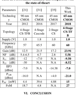
[image:7.595.48.298.411.721.2]Table II presents a comparison chart of various 60 GHz LNAs. The proposed LNA presented achieves the highest gain, FoM andNFminagainst previously reported LNAs. The results indicate that the gain is improved by a factor of 11.20% and NF is improved by a factor of 35.18%.
Table II: Performance summary and comparison with the state-of-theart
VI. CONCLUSION
For LNA design operating in high frequency region greater than 60 GHz, CMOS technology is preferred over all other technologies such as GaN, GaAs and SiGe. In this work four stage CS LNA with TFB topology is designed considering 65 nm CMOS technology. Neutralization technique is adopted
toreduce Millers effect. With TFB technique adopted for LNAdesign bandwidth extension is achieved. The inductors required for TFB can be designed using spiral inductors hence reducing area requirement. The simulation results demonstrated that the designed LNA is suitable for 60 GHz frequency band of (58–64) GHz with highest gain of 23.91 dB, FoM of 27 NF of 5.58 dBand IIP3 of -7 dBm with excellent linearity.
ACKNOWLEDGMENT
The authors would like to acknowledge Keysight technologies for technical support in simulation and modelling of LNA design. We thank Department of Telecommunication Engineering, Bangalore Institute of Technology (BIT), Bengaluru for giving access to ADS software.
REFERENCES
1. L. Tran, R. Isobe, M. Delaney, R. Rhodes, D.J.J Brown, L. Nguyen, M. Le, M. Thompson, and T. Liu,“High Performance, High Yield Millimeter- Wave MMIC LNAs Using InP HEMTs”, IEEE Microwave and Millimeter-Wave Monolithic Circuits Symposium. 3, 1996, pp. 133-136
2. K. Nishikawa, B. Piernas, K. Kamogawa, T. Nakagawa and K. Araki,“Compact LNA and VCO 3-D MMICs Using Commercial GaAs PHEMT Technology for V-band Single-chip TRX MMIC”,IEEE MTT-S Digest. 2012, pp. 1717-1720.
3. K.W. Kobayashi,“An 8-W 250-MHz to 3-GHz Decade-Bandwidth Low-Noise GaN MMIC Feedback Amplifier With > +51-dBm OIP3”,IEEE J. Solid State Circuits. Vol. 47, No. 10, 2012, pp. 2316-2326.
4. B. Floyd, S. K. Reynolds, U. R. Pfeiffer, T. Zwick, T. Beukema and T. Gaucher,“SiGe Bipolar Transceiver Circuits Operating at 60 GHz”,IEEE J. Solid State Circuits.Vol. 40, No. 1, 2005, pp. 156-167.
5. M. Q. Gordon, T. Yao, S. P. Voinigescu,“65-GHz receiver in SiGeBiCMOS using monolithic inductors and transformers”,Si Monolithic Integrated Circuits in RF Systems. 007, pp. 265-268.
6. E. Ragonese, A. Scuderi, G and Palmisano,“A 0.13 µm SiGeBiGMOS LNA for 24-GHz Automotive Short-Range Radar”,Proceedings of the 3rd European Microwave Integrated Circuits Conference. 2008, pp. 510-513.
7. M. Fanoro, S.S. Olokede and S. Sinha,“A low noise and power consumption, high-gain LNA in 130 nm SiGeBiCMOS using transmission lines”,32nd URSI GASS, Montreal, 2017.
8. T. B. Kumar, K. Ma, and K. S. Yeo,“A 60-GHz Coplanar Waveguide-Based Bidirectional LNA in SiGeBiCMOS”,IEEE Microw. Wirel. Components Letters.Vol. 27, No 8, 2017, pp. 742-744.
9. D. J. Cassan and J. R. Long, “A 1-V Transformer-Feedback Low-Noise Amplifier for 5-GHz Wireless LAN in 0.18-μm CMOS”,IEEE Journal Solid State Circuits. Vol. 38, No. 3, 2003, pp. 427–435.
10. R. Fiorelli and E. Peralías,“Semi-empirical RF MOST 5 model for CMOS 65 nm technologies: Theory, extraction method and validation”,INTEGRATION, the VLSI journal. Vol. 52, 2016, pp. 228-236.
11. M. T. Reiha, J. R. Long and J. J. Pekarik,“A 1.2 V Reactive-Feedback 3.1-10.6 GHz Ultrawideband Low-Noise Amplifier in 0.13 μm CMOS”,IEEE Radio Freq. Integr. Circuits Symp.Vol. 1, 2006, pp. 13–16.
12. B.Heydari, M. Bohsali, E. Adabi,and A.M. Niknejad,“Millimeter-Wave Devices and Circuit Blocks up to 104 GHz in 90 nm CMOS”,IEEE J. Solid-State Circuits. Vol. 42, No. 12, 2007, pp. 2893-2903.
Parameters [21] [31] [35] This
Work Technolog
y
90-nm CMOS
65-nm CMOS
45-nm CMOS
65-nm CMOS
Year 2012 2016 2017 2018
Topology 4-Stage CS-TFB
4-Stage Cascode
2-Stage CS
4-Stage CS-TF
B
Supply [V] 1.0 1.8 1.0 1.0
Frequency
[GHz] 57 65.5 60 60
Gain [dB] 12.5 21.5 17.2 23.91
NF [dB] 5.4-6.5 6.7 2.8 5.58
S11 [dB] -12 <7.0 N.A -9.50
S22 [dB] -30 N.A N.A -8.52
IIP3
[dBm] -7.0 N.A -14.38 -7.0
P1dB
[dBm] -16.0 N.A +4.0 -21.0
PDC [mW] 4.4 39.6 4.88 15
13. T. Yao, M. Q. Gordon, K. K.W Tang, K. H. K. Yau, M. A. Yang, P. Schvan and S. P. Voinigescu,“Algorithmic Design of CMOS LNAs and PAs for 60-GHz Radio”,IEEE J. Solid-State Circuits.Vol. 42, No. 5, 2007, pp. 1044-1057.
14. M. Khanpour,“A wideband W-band receiver front-end in 65-nm CMOS”,IEEE J. Solid-State Circuits. Vol. 43, No. 8, 2008, pp. 1717-1730.
15. E. Cohen, S. Ravid and D. Ritter,“An ultra low power LNA with 15 dB gain and 4.4 dB NF in 90 nm CMOS process for 60 GHz phase array radio”,Dig. Pap. - IEEE Radio Freq. Integr. Circuits Symp. 2008, pp. 61–64.
16. S. Pellerano, Y. Palaskas and K. Soumyanath,“A 64 GHz LNA with 15.5 dB Gain and 6.5 dB NF in 90nm CMOS”,IEEE J. Solid-State Circuits,Vol. 43, No. 8, 2008, pp. 1542–1552.
17. Y. L.Wei, S. S. H Hsu and J. D. Jin,“A low-power low-noise amplifier for K-band applications”,IEEE Microw. Wirel. Components Letters,
Vol. 19, No. 2, 2009, pp. 116–118.
18. E. Janssen, R. Mahmoudi, E. V. Heijden, P. Sakian, A. Graauw, A. Pijper and Roermund, “Fully balanced 60 GHz LNA with 37 % bandwidth, 3.8 dB NF, 10 dB gain and constant group delay over 6 GHz bandwidth”, RF Syst. SiRF 2010 - Dig. Pap.2010, pp. 124–127.
19. M. Kraemer, D. Dragomirescu and R. Plana,“A low power high-gain LNA for the 60 GHz band in a 65 nm CMOS technology”,Asia Pacific Microwave Conference Singapore. 2010, pp. 1156-1159.
20. C. C.Huang,“Low-power, high-gain V-band CMOS low noise amplifier for microwave radiometer applications”,IEEE Microw. Wirel. Components Letters.Vol. 21, No. 2,2011, pp. 104–106.
21. P. Y. Chang, “An ultra-low-power transformer-feedback 60 GHz low-noise amplifier in 90 nm CMOS”,IEEE Microw. Wirel. Components Letters.Vol. 22, No. 4, 2012, pp. 97–199.
22. J. R. Long,“Monolithic transformers for silicon RF IC design”, IEEE J. Solid-State Circuits.Vol. 35, No. 9, 2000, pp. 1368–1382.
23. H. M. Cheema, “Monolithic transformers for high frequency bulk CMOS circuits”,9th Top. Meet. Silicon Monolith. Integr. Circuits RF Syst. SiRF’09 - Dig. Pap.,Vol. 1,2009, pp. 112–115.
24. R. P. Jindal,“Compact noise models for MOSFETs”,IEEE Trans. Electron Devices. Vol. 53, No. 9,2006, pp. 2051–2061.
25. M. Varonen, M. Karkkainen and K. Halonen,“Millimeter-wave amplifiers in 65-nm CMOS”,In 33rd ESSCIRC,2007, pp. 280–283.
26. V. Dimitrov, J.B. Hengan and K. Timp, “Small-signal performance and modeling of sub-50 nm nMOSFETs with fT above 460
GHz”,Solid State Electronics.Vol. 52, 2008, pp. 899-908.
27. A. Wang, L. Li and T. Cui,“A Transformer Neutralization Based 60 GHz LNA in 65 nm LP CMOS with 22 dB Gain and 5.5 dB NF”,
IEEE Radio Frequency Integrated Circuits Symposium (RFIC).2013, pp. 1111-1114.
28. D. S. Siao, J. C. Kao and H. Wang,“A 60 GHz Low Phase Variation Variable Gain Amplifier in 65 nm CMOS”, IEEE Microw. Wirel. Components Letters, Vol24, No. 7, 2014, pp. 457-459.
29. H. Mizutani, E. Taniguchi, M. Taniguchi, R. Inagaki, S. Inagaki, N. Suematsu, T. Takagi and K. Tsubouchi,“An Optimum Inductive Matched Cascode LNA in 60 GHz Band”,IEEE International Symposium on Radio-Frequency Integration Technology (RFIT).2015, pp. 20-30.
30. J. O. Plouchart, F. Wang, A. Balteanu, B. Parker, M. A. T Sanduleanu, M. Yeck, V. H. C. Chen, W. Woods, B. Sadhul, A. V. Garcia1, X. Li and D. Friedman, “A 18mW, 3.3dB NF, 60 GHz LNA in 32 nm SOI CMOS Technology with Autonomic NF Calibration”,IEEE Radio Frequency Integrated Circuits Symposium,2015, pp. 319-322.
31. F. Meng, K. Ma, K. S. Yeo, C. C. Boon, X. Y. J. Sun, G. Feng and S. Xu,“A Compact 57–67 GHz Bidirectional LNAPA in 65-nm CMOS Technology”,IEEE Microw. Wirel. Components Letters.Vol. 26, No. 8, 2016, pp. 628-630.
32. K. Y. Kao, D. R. Lu, J.C. Kao and K.Y. Lin, “A 60 GHz Variable-Gain Low-Noise Amplifier with Low Phase Variation”,IEEE International Symposium on Radio-FrequencyIntegration Technology (RFIT).2016, pp. 1-3.
33. M. M. Fouad, M. M. Aboudina, A. Eladawy and E. A. Hashish,“MmWave LNA Using Feedback Guanella Transmission Line Transformer”,IEEE 59th International Midwest Symposium on Circuits and Systems (MWSCAS).2016, pp. 1-4.
34. S. Guo, T. Xi, P. Gui, D. Huang, Y. Fan and M. Morgan,“A Transformer Feedback Gm-Boosting Technique for Gain Improvement and Noise Reduction in mm-Wave Cascode
LNAs”,IEEE Transactions on Microwave Theory and Techniques.
Vol. 64, No. 7, 2016, pp. 2080-2090.
35. S. Subramaniam, T. Shinde, P. Deshmukh, M. S. Shamim, M. Indovina and A. Ganguly,“A 0.36 pJ/bit, 17 Gbps OOK Receiver in 45-nm CMOS for Inter and Intra-Chip Wireless Interconnects”,30th IEEE international System-On-Chip Conference (SOCC).2017, pp. 132-137.
36. R. Chikkanagouda and Cyril Prasanna Raj P, “60 GHz LNA Design with Inductive Source Degeneration in 65 nm CMOS Technology”,
In: Hemanth J., Fernando X., Lafata P., Baig Z. (eds) International Conference on Intelligent Data Communication technologies and Internet of Things (ICICI) 2018. Lecture Notes on Data Engineering and Communications Technologies, Springer, Cham, 26.2019, pp. 363-370.
37. D. M Pozar,Microwave Engineering, 2nd edition. John Wiley & Sons, Inc.
38. L. O. Chua, C. A. Desoer, E. Kuh E. S., Linear and Nonlinear Circuits. McGraw-Hill.(1987).
39. S. A. Maas, Nonlinear Microwave and RF Circuits. Artech House (2003).
40. G. Gonzales, Microwave transistor amplifier. Prentice Hall. (1997)
41. Predictive Technology Model, Latest Models. http://ptm.asu.edu/modelcard/2006/65nm_bulk.pm (accessed on 18 June (2018).
AUTHORSPROFILE
Mr. Rajendra Chikkanagouda received the M. Tech degree in Digital Electronics & Communications from Visveswaraya Technological University, Karnataka, India and B.E. degree in Electrical & Electronics from Kuvempu University, Karnataka, India; He worked in the CPRI, Bengaluru and MRO-TEK Limited R & D Division as a product development Lead where he was responsible for designing and development of networking products. His research interests are in the design of Networking Products, Digital System Design, Analog and Mixed mode and millimeter-wave IC building blocks. He is currently pursuing the Ph.D. degree in electrical engineering at Visvesvaraya Technological University.