Synchronization Overhead in SOC Compressed Test
Paul Theo Gonciari, Member, IEEE, Bashir Al-Hashimi, Senior Member, IEEE, and Nicola Nicolici, Member, IEEE,Abstract— Test data compression is an enabling technology for low-cost test. Compression schemes however, require communication between the system under test and the automated test equipment. This communication, referred to in this paper as synchronization overhead, may hinder the effective deployment of this new test technology for core-based systems-on-a-chip. This paper analyzes the sources of syn-chronization overhead and discusses the different trade-offs, such as area overhead, test time and automatic test equipment extensions. A novel scalable and programmable on-chip distribution architecture is proposed, which addresses the synchronization overhead problem and facilitates the use of low cost testers for manufacturing test. The design of the proposed architecture is introduced in a generic framework, and the implementation issues (including the test controller and test set preparation) have been considered for a particular case.
Index Terms— DFT, low cost test, test data compression, core-based SOC
I. INTRODUCTION
Driven by high transistor density the semiconductor industry is seeing an increase in transistor test cost, which as emphasized in the international technology roadmap for semiconductors (ITRS) [1] may even exceed the cost of manufacturing it. The increase in test cost is attributed to mainly two factors: (a) the high cost of the automated test equipment (ATE), and (b) high test times. On the one hand, to account for high pin count, for high test pin accuracy and for the high volumes of test data (VTD), the ATE’s are equipped with cutting edge equipment, which considerable drive their cost. On the other hand, using existing ATE infrastructure, due to the high volume of test data and limited ATE bandwidth, the test time is becoming increasingly high [2]. To reduce the cost two main trends have been merged:(i)the usage of low-cost testers to reduce the cost of the ATE [3]; and (ii)the usage of test resource partitioning schemes, which by adding on-chip test resources can reduce the test application time and bandwidth requirements [4, 5].
Test resource partitioning has received considerable attention in recent years due to it’s inherent property of reducing the load on the tester, and hence endorsing a low-cost ATE test strategy. In this paper we address one fundamental issue in test resource partitioning in general, and test data compression in particular: communication between the ATE and the on-chip test infrastructure, required for (a) transferring test data to and from the ATE, and for (b) controlling the flow of data, e.g., to start/stop the flow of data.
Test data compression (TDC) is a two step process which aims at reducing the volume of test data required to test a chip [6]. In the first step, the initial test set (TD) is compressed by means of
a compression algorithm and the resulted compressed test set (TE)
stored on the ATE; while in the second step, the compressed test set is sent to the chip under test (CUT) and decompressed on-chip by
Manuscript received November 2003; revised February 2004.A preliminary version of this paper has been published in IEEE European Test Workshop (ETW) 2002. This paper was recommended by xx.
Paul Theo Gonciari and Bashir Al-Hasimi are with the Electronic Systems Design Group, School of Electronics and Computer Science, University of Southampton Southampton, SO17 1BJ, U.K (e-mail: [email protected]; [email protected]). They wish to acknowledge EPSRC (UK), which partially supported this work under grant GR/S41135.
Nicola Nicolici is with the Computer-Aided Design and Test Research Group, Department of Electrical and Computer Engineering, McMaster Uni-versity,Hamilton, ON L8S 4K1, Canada (e-mail:[email protected]).
means of an on-chip decoder. As will be seen in the following section, both data and control communication requirements of some TDC schemes can be considerable (i.e., a large number of ATE channels are required). Furthermore, based on the type of on-chip decoder (i.e., serial or parallel) some of the TDC schemes may also incur hardware penalties. Throughout the paper we will refer to communication requirements and hardware penalties as synchronization overhead.
This paper analyzes synchronization overhead for different TDC schemes, and provides a generic solution to reduce it. The proposed solution does not impose changes to existing decoders and it provides easy design flow integration. The solution eases system level test as it is scalable (i.e., it can be extended to as many cores as required) and programmable (i.e., the characteristics of each core test, such as the type of test, the length of the internal scan chain can be changed at run-time). In particular, the proposed approach is illustrated for the Variable-length Input Huffman Coding (VIHC) method [6].
The remainder of this paper is organized as follows. In the follow-ing section previous approaches to reduce synchronization overhead are analyzed. In Section III, the proposed approach is presented, and experimental results are given in Section IV. In Section V practical implementation issues of the distribution architecture introduced in this paper are discussed, and Section VI concludes the paper.
II. THE IMPORTANCE OF SYNCHRONIZATION IN TEST DATA COMPRESSION
As will be seen in this section, in general, synchronization overhead includes one or more of the following:(i)the use of multiple ATE channels; (ii) adapting ATEs to start and stop the data stream in real time;(iii)on-chip serialization units; and(iv)extensions to the device interface board (DIB). Each of the above influences the cost of test and diminishes the benefits of TDC, as explained next:
• the use of multiple ATE channels(i), diminishes the effective-ness of reduce pin count test (RPCT) and lead to inefficient ATE resource usage;
• the adaption of ATEs to start and stop the data stream in real time(ii) requires ATE extensions, such as source synchronous buses, which can increase cost;
• the usage of on-chip serialization units (iii) increases the area overhead on-chip;
• the extensions to the DIB(iv)may lead to prohibitive high DIB costs due to the complex designs of DIB when high frequency SOCs are tested [1, 7, 8].
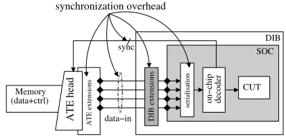
When all of the above are included, the ATE – DUT interface is illustrated in Figure 1. As shown above, to cope with communication requirements, there is usually a hardware component required. In addition to the immediate cost of the hardware, synchronization overhead may also incur additional test costs. For example, when multiple ATE channels are used, the volume of test data is given by the depth of the longest channel multiplied by the number of channels. Hence, test data penalties are incurred. Also, the starting and stopping of the ATE data stream has to be programmed, increasing the test preparation time. In addition, whenever the ATE data stream is stopped, but the test session is not finished, the effective test time is also increased.
on−chip decoder
SOC DIB
data−in Memory
(data+ctrl)
ATE head ATE extensions
serialisation
sync
synchronization overhead
CUT
[image:2.612.70.276.53.153.2]DIB extensions
Fig. 1. Test data compression environment with synchronization overhead
cost effective solutions in order to take full advantage of the benefits of TDC. In this section the above issues will be detailed and an analysis of previous approaches, which have targeted synchronization overhead, will be provided.
A. Sources of synchronization overhead
As illustrated in the previous section, synchronization overhead is due to the second step of TDC, on-chip decompression. Therefore, firstly we illustrate a generic on-chip decoder, then we review TDC approaches from the decoder’s perspective, and finally we analyze decoders based on their synchronization overhead requirements.
An on-chip decoder can be conceptually seen as comprising a code
identifier and a pattern generator (see Figure 2). The “data source”,
in the figure, provides the compressed test set (TE) to the decoder’s
“data in” and can be either on-chip or off-chip. Note that, while the primary data source is on the ATE, some decoders require on-chip se-rialization units which will therefore become their “data source”. The “sync” lines ensure the synchronization between the on-chip decoder and the “data source”, and can comprise ATE clock signals, start/stop signals from the decoder to the ATE or to the on-chip source, and special clock signals. The output of the decoder (“data out”) drives the core’s internal scan chain synchronously with the “scan clk”. The compressed data is sent from the ATE to the DIB at the ATE operating frequency ( fate), and the decoder outputs data with the chip
test frequency ( fchip).
1) Test data compression approaches: For the purpose of this
paper, TDC methods are broadly classified into two categories: (i)
[image:2.612.325.550.53.98.2]methods which exploit the spareness of care bits in the test set [4, 9–11] and(ii)methods which exploit the regularities of the test set [6, 12–14]. The relevant aspects of the above approaches are their decoders. For the first category(i), the decoders tend to have a small number of inputs (n), and a large number of outputs (m). For the second category (ii), the decoders tend to have a small number of inputs, and a small number of outputs (usually 1), however the outputs are driven at a frequency higher than the inputs. The above conditions are discussed in detail in the following paragraphs.
(i) For the first category, two aspects are important from the compression perspective. Firstly, to increase compression ratio, it must be ensured that m>>n, and secondly, any combination required
at the decoder’s outputs must be generated by an input sequence (over one or more clock cycles). While the first issue is solved by adding an xor network (or phase shifter) [4, 9, 10] at the outputs of the decoder, the second problem requires careful consideration. Assume, for example, that one particular pattern can not be generated at the outputs of the decoder (i.e., there is pattern lockout condition). If this condition is not resolved, the fault coverage could be affected, and hence, the approaches would render impractical. Proposed solutions to deal with this condition are three fold: (a) provide an extra input which notifies the decoder when the data should be loaded into the scan chains [9]; (b) integrate the compression method with an
code identifier
data source
TE
data in chip clk
sync Core
scan chain TD
pattern generator scan clk data out
Fig. 2. Generic on-chip decoder
automatic pattern generator (ATPG), and ensure that patterns that can’t be justified by the decoder will not be generated by the APTG [4, 10]; or, (c) account for pattern lockout by prefixing the data sent to the decoder with information that distinguishes between compressed data, and uncompressed data [11].
Hence, in order to deal with the pattern lockout condition, the above approaches imply some overhead: in terms of hardware re-source, such as the addition of extra inputs; and in terms of test time and test data resources, through the addition of padding bits. Thus, whilst this first category it taught of as synchronization overhead
free, the overhead issues are dealt with inherently by the approaches
in order to alleviate the pattern lockout condition, and therefore not covered in this paper.
(ii) Since the methods in the second category are build around coding schemes, these will implicitly guarantee the generation of the required pattern at the output of the decoder. Hence, these methods do not suffer from the pattern lockout condition, however, in order to reduce test application time (TAT), when the decoder has 1 output, the pattern generator should operate at a frequency greater than fate.
This is explained as follows: if the pattern generator is operating at fate, then the time required to generate the initial test set (TD)
will be the same as if TD is directly transported from the ATE
to the CUT. In addition, the code identifier unit adds its latency, which is the time required to identify a code. Thus, with the pattern generator running at fatethe TAT is not reduced, rather it is actually
increased! Therefore, to reduce TAT the ratio between the on-chip test frequency ( fchip) and the ATE operating frequency must be exploited
(α= fchip
fate). Exploiting the frequency ration brings forth a number of synchronization problems as will be seen in Section II-A.2.
It is important to note that the decoder has to operate at a frequency
fchipgreater than fate; and while, for simplicity, we also assume that
the scan chains are fed at fchip, this is not mandatory. For example,
the output of the decoder could feed a shift register, and this could then load data into a multiple scan chain core at a frequency smaller than fchip, or even than fate. It should be also noted that when the
pattern generator can generate any pattern in one chip test clock cycle, there is no need to exploit the frequency ratio [14].
2) On-chip decoder’s characterization: Based on the
dependen-cies between the code identifier and the pattern generator (see Figure 2), on-chip decoders can be characterized as serial (i.e., during the decompression of the current code, no new code can be identified) or parallel (i.e., the decompression of the current code and the identification of a new one can be done simultaneously). To illustrate the fundamental distinction between serial and parallel decoders, and at the same time to illustrate the main source of synchronization overhead, in Figure 3 the functionality of the two types of decoders is exemplified considering a frequency ratio of α=2. The serial decoder receives data at the fchipfrequency and it generates data at
the fchipfrequency, while the parallel decoder receives data at the fate
frequency and generates data at the fchipfrequency. The stopping of
1
0 1 0
0 1 2 3 4 5
CI ATE clock chip test clock
PG
α = 2:1
0 0
STOP
(a) Serial decoder
0 0 1 0 0
0 1 2 3 4 5
CI ATE clock chip test clock
PG 1
6 α = 2:1
0 0
STOP
0
[image:3.612.112.295.62.194.2](b) Parallel decoder
Fig. 3. Serial and parallel decoders explained
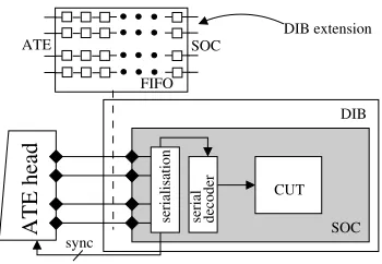
ATE head
syncDIB extension
ATE SOC
serialisation serial decoder
CUT
SOC DIB FIFO
(a) Serial decoder’s synchronization overhead
FIFO
ATE SOC DIB extension
ATE head
syncDIB SOC
CUT parallel dec
(b) Parallel decoder’s synchronization overhead
Fig. 4. Synchronization overhead for serial and parallel decoder
in the figure. The stopping of the ATE data stream is illustrated for a parallel decoder in Figure 3(b). It can be seen in the figure that the code identifier can work independently from the pattern generator, i.e., the CI can receive data while the PG generates data, and that the ATE data stream is stopped only when required. The synchronization overhead for the two types of decoder are analyzed next.
(i) When a serial decoder is employed, in order to exploit α
the entire decoder operates at fchip. Hence, the “data source” is
constrained to using techniques such as those described in [15] and [16] for providing data at fchip. This implies the usage of multiple ATE channels and a serialization unit on-chip or on the DIB. This is
exemplified in Figure 4(a), where forα=4, the ATE channels and the serialization unit are illustrated. In addition, when the current pattern is generated no more data can be processed by the code identifier, hence, the “sync” lines need to notify the ATE to stop sending data (see Figure 3(a)). Since, some ATEs are not capable of starting/stopping the data stream immediately and require a number of clock cycles to change the state of the channel, the DIB must account for this latency. Therefore, the interface between the ATE and the chip requires a first-in first-out (FIFO)-like structure to solve this problem. The number of elements in the FIFO is given by the maximum number of clock cycles needed to start/stop the data stream on the channels. The FIFO-like structure is marked in the figure as DIB extension. Hence, a serial decoder will not only requireαinput ATE channels, but also anα bit wide FIFO-like structure.
(ii) When a parallel decoder is employed, the code identifier can
receive data at fate, and the pattern generator can generate data at fchip. Hence, the decoder implicitly exploits the frequency ratio, and
therefore only one ATE channel is required for feeding data to the
decoder as shown in Figure 4(b).
For a parallel decoder, consider αmax the frequency ratio which
allows the pattern generator to generate the longest pattern in the number of ATE clock cycles needed by the decoder to identify the shortest codeword. For example, if the longest pattern has 6 bits, and the shortest codeword 1 bit, the decoder has to generate data 6 times faster than it receives, henceαmax=6.
Therefore, if α is greater than, or equal to, αmax, no stop
noti-fications will be send to the ATE; however, if the frequency ratio is less than αmax, the on-chip decoder will notify the ATE to stop
sending data. As also noted earlier, the ATE has a certain latency to starting/stopping the data stream on a channel and therefore a FIFO-like structure is required, which is marked in the figure as DIB extension. Hence, when compared to a serial decoder, the parallel decoder has less synchronization overhead with respect to the interface between the ATE and the DUT. However, since the two units (the code identifier and the pattern generator) can work independently explicit communication between the two units is required, and hence, parallel decoders tend to have larger area requirements [6]. Since by redesigning the serial decoder, a parallel version can be envisioned, this paper will focus on reducing synchronization overhead for parallel decoders.
[image:3.612.114.289.240.361.2]pattern A B C D
occ. code−2
10 1
01 001 000
11 10 01 00
VTD (bits) 25 32
code
3 1 2
(a) Dictionary
wmin=1 0
0
0 1
1
D C
B A
1
(b) Initial Huffman tree
wmin= 2
D C B A
0 1
1 0 1 0
[image:4.612.50.177.64.156.2](c) Tailoring for wmin=2
Fig. 5. Tailoring the compression method
the data stream within the ATE memory. In addition, as it will be seen in Section III-A, halting the ATE data stream is not periodic and therefore, the ATE must know exactly when the data stream must be started and stopped. This can lead to prohibitively larger ATE programs, thus larger memory requirements, and it will not reduce the TAT.
To summarize this section, it becomes clear that synchronization overhead introduces a trade-off between the effectiveness of test data compression and cost (i.e., hardware overhead, test time, volume of test data). Addressing this issue is therefore of primary importance in test data compression.
B. Analysis of previous approaches to reduce synchronization over-head
As illustrated in the previous section, depending on the type of decoder, different synchronization schemes are required. In the fol-lowing paragraphs we analyze synchronization overhead implications of the compression methods proposed in [12, 13].
Selective coding (SC) [13]: employs a parallel on-chip decoder
to decompress the test set on-chip. The SC decoder uses a modified Huffman finite state machine (FSM) as the code identifier, and a serializer as the pattern generator. The code identifier is receiving data at fate, and the pattern generator generates data at fchip. Hence,
synchronization with the ATE is required ifα<αmax(see Section
II-A). To solve this problem [13] tailors the compression method to suite
α. Withαmax=wbmin [13], where b is the block size and wminis the
minimum length codeword, the synchronization overhead is reduced if wmin≥αb. Therefore, to reduce the synchronization overhead for a
given block size, wminhas to be increased. This can be done in two
ways as follows.(a) If the number of patterns chosen for selective coding do not yield the required wmin, the number of patterns can
be increased. While this could increase compression ratio, it also increases the on-chip decoder area considerably [13]. (b)A second approach, assuming a fixed number of patterns, is to increase wmin
by manipulating the Huffman tree used to obtain the selective code, and appending bits to the codewords which are shorter than required. This, however, has a direct impact on the compression ratio since increasing wminincreases the average codeword length, which reduces
compression ratio leading to test data penalties, as illustrated next. Consider four patterns A,B,C and D, and their number of
occur-rences as given in Figure 5(a) in the first two columns. Based on these two columns the Huffman tree can be built. The corresponding Huffman tree is illustrated in Figure 5(b). Based on the Huffman tree, the codes are derived and shown in the third column in Figure 5(a). It can be observed that wmin=1. If for example, b=4 andα=2,
then based on the previous formula, wmin≥ 42 =2 in order to
eliminate the synchronization overhead. Tailoring the compression method to obtain wmin=2 is illustrated with Figure 5(c), and the
codes obtained based on this new tree are shown Figure 5(a) in
FIFO
ATE SOC
ATE head
DIB
CUT
sync
DIB extension
FSM
demultiplexer
serial dec
serial dec serial dec serial dec
CUT CUT CUT
[image:4.612.303.558.72.328.2]SOC
Fig. 6. Interleaving architecture based on [12]
the fourth column. Summing up, the VTD for the two codes is 25 and 32 bits respectively. Hence, it becomes clear that tailoring the compression method can lead to an increase in VTD. It should be noted that if b=6, a wminof 3 can only be obtained if the codes are
padded.
Thus, the synchronization overhead is reduced at the expense of test data penalties and a frequency ratio dependent on-chip decoder. Hence, if testing is sought at different frequencies, the ATE is constrained to operate at a new frequency such that the frequency ratio between the CUT and the ATE remains the same. With already limited ATEs, the on-chip decoders should fully exploit the ATE capabilities and not further constrain them. Therefore, Section III-A proposes to tailor the compressed test set, and not the compression method, for a givenα. In addition to obtaining similar and smaller test sets than the above approach with no changes to the on-chip decoder, tailoring the compressed test set is generally applicable to decoders which require a FIFO-like structure.
Golomb [12]: uses a serial decoder to provide decompressed test
L0 = 1 1 000
L1 = 01 1 001
L2 = 001 1 010
L3 = 0001 1 011
L4 =0000 4 1
Code Pattern Occurrence
(a) Dictionary
= 26 bits = 16 bits tinit tcmp
h m = 4
t cmp
t init 1 01 0000 0000 0000 0001 0000 001 1 011 1 001
000 1 1 010
(b) Test sets
Fig. 7. VIHC - an example [6]
noted that, due to its serial nature the decoder proposed in [18] has the same requirements as the Golomb decoder and the partitioning scheme proposed in [19] also requires also a FIFO-like structure.
Since Golomb’s decoder is a serial decoder, the FSM will have to explicitly control each decoder connected in the interleaving archi-tecture. In order to synchronize the FSM and the decoders, changes to the on-chip decoders are necessary. In addition, the interleaving architecture imposes the following two restrictions. Firstly, all the cores which are driven by it have their test sets compressed using the same group size; and secondly, the number of cores tested using this architectures is constrained by the group size [17]. These two restrictions are due to the exploitation of the above mentioned Golomb decoder’s property. Also, these two restrictions will eliminate the need for the DIB extension at the expense of imposing constraints on the system integrator. To remove the above restrictions for multiple core SOC test, Section III-B proposes a distribution architecture which does not require any changes to the on-chip decoders, and it is also scalable and programmable.
III. PROPOSED APPROACH FOR REDUCING SYNCHRONIZATION OVERHEAD
The solution proposed to reduce the synchronization overhead is divided into two parts. The first part, illustrated in Section III-A, reduces the FIFO-like structure by introducing dummy bits within the compressed test set, hence tailoring the compressed test set for a given frequency ratio. The second part, illustrated in Section III-B, exploits the inserted dummy bits and provides a complete solution for system level test using a distribution architecture.
The proposed solution has two distinctive features: it is applicable to decoder which requires a FIFO like structure, and it provides a complete RPCT scenario for SOCs with low storage requirements and low TAT without any constraints or changes to the test or interface equipment, e.g., ATE or DIB. In this section we will introduce the proposed approach using the Variable-length Input Huffman Coding (VIHC) scheme [6], which is briefly revised next.
The VIHC scheme splits the test set into runs of ’0’s of length smaller than, or equal to, a group size (mh). The obtained patterns
are then encoded using Huffman coding. This is exemplified, for
mh=4, in Figure 7, where one test vector is processed. Using VIHC
the initial test vector (tinit) is compressed (tcmp) (see Figure 7(b)
where the codewords are delimited through spaces). The dictionary employed in the compression process is illustrated in Figure 7(a). The VIHC method uses a parallel on-chip decoder comprising a Huffman decoder as the code identifier and a control and generation unit (CGU) as the pattern generator. When the Huff-decoder identifies a codeword, the CGU starts generating the pattern after two on-chip clock cycles. For the distribution architecture proposed in this paper, the following signals are of interest. The ATE sync represents the signal used by the CGU to notify the ATE to stop sending data, the
FSM clk represents the clock used to drive the code identifier unit,
the dec clk represents the CGU clock, the data out represents the data output of the decoder, and the scan clk represents the clock generated by the CGU to control the scan chains.
A. Tailoring the compressed test set
The optimum frequency ratio for the VIHC decoder is given by
αmax=wmminh , where wminis the minimum codeword length [6]. Hence ifα<αmax, the CGU will notify the ATE to stop sending data. This
is exemplified next, for the case considered in Figure 7.
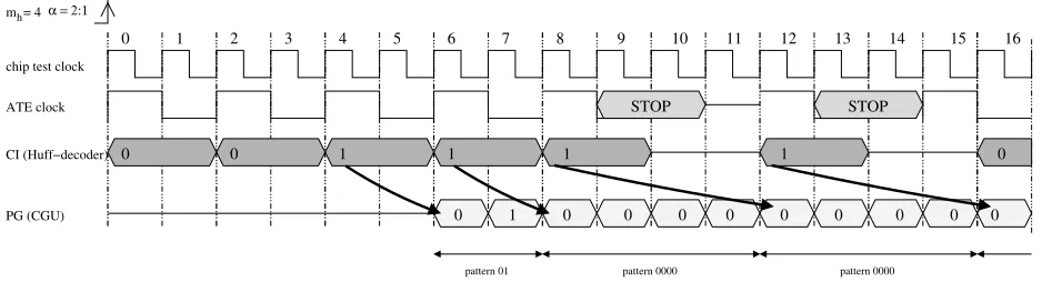
Example 1 Based on Figure 7, it can be derived thatαmax=41=4.
To illustrate the stopping of the data stream, for the remainder of this sectionα=2. For the example in Figure 7(b), Figure 8 shows a timing diagram when tcmpis decompressed using the VIHC decoder.
The arrows in the figure point from the compressed test bit, which lead to the identification of a codeword, to the clock cycle when the generation of the corresponding pattern starts. The diagram captures the activity of the decoder’s parts starting with the second codeword from tcmp(001 in Figure 7(b)). The reference clock is the on-chip test
clock. The time frame of interest is from the 6th to the 15th clock cycle, where there are two stop cycles in which no data from the ATE is processed. At the 6th clock cycle the codeword “1” is identified. The CGU, at clock cycle 8, starts generating the corresponding pattern “0000”. However, since the next codeword is “1” there are not enough clock cycles to generate the pattern, i.e., the code identifier requires 1 ATE clock cycle to determine the next codeword, while the CGU requires 4 on-chip clock cycles, or 2 ATE clock cycles, to generate the current pattern. Hence, the ATE will be stopped for 1 clock cycle. Similar for clock cycle 13.
The reason for stopping the ATE is to make sure that no data is lost while the on-chip decoder is unable to process it. However, if care is taken to ensure that the data which could be lost is not relevant, there is no need to stop the ATE in the first place. To achieve this the compressed test set is tailored for the current frequency ratio. This works as follows. For the number of ATE clock cycles in which the CGU sets ATE sync to low, thus notifying the ATE to stop sending data, dummy (D) bits are inserted in the compressed test set. For a given frequency ratio (α) the number of dummy bits is obtained using
d|Li|−wi+1·α
α e, where |Li|represents the length of the current pattern
and wi+1represents the length of the next codeword [6]. Hence, since there is no need to stop the ATE, the FIFO-like structure can be removed thus eliminating the synchronization overhead. Since these dummy bits will not be processed by the decoder they will not affect the correct generation of the decompressed test set. Applying this strategy to the entire tcmp, t
0
cmp=000 001 1 1D 1D 011 1D 010 is
h
m = 4α = 2:1
0 0
0
pattern 01 pattern 0000 pattern 0000
0 1 2 3 4
CI (Huff−decoder)
5 6 7 8 9 10 11 12 13 14
ATE clock chip test clock
PG (CGU)
16 15
0 0 0 0
1 0 0 0
STOP
0 0 1 1
STOP
[image:6.612.72.541.56.183.2]1 1 0
Fig. 8. Timing diagram to illustrate the stopping of the data stream
the CGU, the size of the tailored test set in bits will equal the TAT in ATE clock cycles.
When compared to tailoring the compression method (as illustrated in Section II-B), this approach is especially suitable when the ratio between mh and α is rather large (e.g. mαh is 4 or 8). This is
due to the large number of padding bits required by tailoring the compression method. For example assume that when the test set is compressed using mh=16, wmin=1. If α=2, then in order to
reduce synchronization overhead, wminwill be 8. Thus, tailoring the
compression method will increase all the codewords to be of size 8, hence reducing compression ratio.
Since the proposed approach does not change the code used for compression nor the on-chip decoder, it is generally applicable to methods which require a FIFO-like structure for synchronization. Despite this advantage, tailoring the compressed test set and tailoring the compression method increase the volume of test data stored on the ATE. Hence, these methods bring forth a trade-off between the synchronization overhead and the amount of memory required on the ATE. To solve this problem in the following section a distribution architecture to test multiple cores is proposed.
B. Distribution architecture for multiple core test
Testing multiple cores using only one ATE channel implies ex-ploiting the clock cycles when the decoder corresponding to a core is not capable of processing data. For example, when using the MinTest [20] test set for the s13207 full scan ISCAS89 [21] benchmark circuit, and applying VIHC with mh=8, the compressed test set is 38123
bits. However, the TAT for α=2 is of 89646 ATE clock cycles. Hence, there are 51523 ATE clock cycles in which the decoder is not processing data, or there are 51523 dummy bits in the tailored compressed test set stored on the ATE.
To explore these dummy bits for multiple core test using one ATE channel, the following steps are performed: (a) the core’s compressed test sets are merged into one composite test set, (b) one decoder per core is used and (c) the necessary, core and decoder, selection hardware is added. These steps are illustrated in the next example.
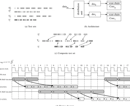
Example 2 Assume a system composed out of two cores (Core0
and Core1) and their corresponding decoders (dec0 and dec1), with the test sets given by TD0 and TD1 in Figure 9(a). Both test sets have been compressed using the codes given in Figure 7(a) and tailored for a frequency ratio ofα=2 (Tt0and Tt1in Figure 9(a)). It can be
observed that, in order to reduce the synchronization overhead, both test sets require three dummy bits. Using only one ATE channel the test data can be send to the cores by careful selection of the decoder which receives data. This is illustrated generically in Figure 9(b) with the distribution unit, which will be detailed later in this section. The
unit is receiving data from the ATE at fate, using one ATE channel,
and sends data to the selected decoder at fate. Hence, the data send to
the distribution unit has to correspond to the selected decoder. This is achieved by generating a composite test set (TC) which matches
the distribution’s unit functionality, as detailed next.
Starting with the tailored compressed test sets, the composite test set is generated as illustrated in Figure 9(c). Firstly, the bits from the first test set are copied into TCup to the first dummy bit. At this point,
the next test set is chosen, Tt1(bold is used to represent the data from Tt1), and the bits up to the first dummy bit are copied into TC. To
illustrate the implications in the distribution’s unit functionality when the changing of the test set occurs, a timing diagram is presented in Figure 9(d). Each decoder has been represented by the code identifier (CI) and the pattern generator (PG) in the figure. It can be seen that at the 4th on-chip clock cycle CI1 becomes active. Hence, instead of sending a dummy bit to decoder CI0as in the case of the tailored test set, useful test data is sent to decoder CI1. Since, the test data from
T1
t has been added to TC, CI1will receive the correct compressed test bits. While switching of the test sets based on the occurrence of the dummy bits is usually performed, there are some exceptions which have to be accounted for. For example, bit stream “1D 011 1D” in the tailored compressed test set for T0
t was copied into TC without the
first dummy bit. This is due to the fact that when the first codeword 1 from the above bit stream is received by CI0, the pattern generator does not generate any more data, and therefore it can commence the generation of the pattern immediately after the codeword has been identified (clock cycle 14 in Figure 9(d)). Note that this is contrary to Figure 8 (clock cycle 13), where the pattern generator was still busy generating the pattern corresponding to a previous codeword, and therefore the dummy bit was inserted in the T0
t . In general, if
|Li|−wi+1·α
α is negative then there is no need to insert the dummy bit into TC. It is important to note that, if the number of bits copied into TC are not enough to account for the number of dummy bits from
the previous test set, and if there are no more test sets available, then dummy bits are inserted into TC.
A distribution architecture which can make use of the composite test set as generated above is given for the general case of k cores in Figure 10. The distribution architecture comprises: a log2k bit
counter, a k : 1 multiplexer, a log2k : k decoder and a k bit config-uration register (conf reg). The counter drives the log2k : k decoder
and the k : 1 mux. The eni output of the log2k : k decoder is high, enabling the corresponding decoder (deci) if the log2k counter has
the appropriate value. The synchronization elements (sync elem), illustrated in the figure, represent blocks of logic which ensure that the code identifier of decoder deci will not receive the FSM clk if eni is low. In addition, in order to completely disable the decoder
Tt1 TD1 TD0 Tt0
1 01 0000 0000 0001 0000 001
1 0000 0001 0000 0000 001
000 001 1 1D 1D 011 1D 010 0000
0000
000 1 1D 011 1D 1D 010
(a) Test sets
dec0 scan chain
distribution unit
Core1 scan chain dec1
datain Core0
(b) Architecture
TC
T1 t T0 t
1
000 001 1 1 000 1 1 011 1 011 1 010 1010
000 1 1D 011 1D 1D 010
000 001 1 1D 1D 011 1D 010
(c) Composite test set
h m = 4α = 2:1
0 0 0 0
0 0 0 0 0
0
0 0 0 0
0 1 2 3 4 5 6 7 8 9 10 11 12 13 14 15
ATE clock chip test clock
CI0 (Huff−decoder)
PG0 (CGU)
17 16
0 0
PG1 (CGU) 1
CI1 (Huff−decoder) 0 0 0 1
1
1 0
1
1
[image:7.612.79.534.61.432.2](d) Timing diagram
Fig. 9. Distribution architecture for two cores
the dec clk signal (as illustrated with add. gating in Figure 10). This, however, is not necessary for the VIHC decoder [6].
After reset, the counter is selecting decoder dec0. As long as the
ATE sync signal is high, dec0processes data from datain. Once the ATE sync is set to low, the counter will increment enabling the next
decoder which has the ATE sync line high to process data from the ATE. It should be noted that the ATE sync is set low when the pattern generator is still busy processing the previous pattern and can not commence the generation of the new one. This state corresponds to the changing of test sets as illustrated in Example 2.
To summarize, for a system with k cores, employing this ar-chitecture implies the following steps. Firstly, each core’s test set is compressed such that the compression ratio, area overhead and TAT meet the system’s constraints. Secondly, for the decoders which have αmax greater than the available frequency ratio, the tailored
compressed test sets are determined. Finally, the tailored compressed test sets are merged together into a composite test set (TC) as
illustrated with Example 2. If there are test sets which do not require tailoring, and dummy bits have to be inserted into TC, then the
distribution architecture can be extended with one more decoder. This decoder corresponds to the test sets which does not require tailoring. When all the decoders connected to the distribution architecture are busy, then the data can be redirected to this separate decoder, and thus no dummy bits are required. It should be noted that, the size of
TCis lower bounded by the sum of sizes of the initially compressed
test sets and upper bounded by the sum of the sizes of the tailored compressed test sets. This is because, if no dummy bits are inserted into the composite test set, the size of the composite test set is given by the sum of sizes the initially compressed test sets. If however, dummy bits are required, the number of dummy bits is always smaller than the sum of the dummy bits in the tailored compressed test sets. The algorithm for computing the composite test set has a com-plexity which is linear in the size of the compressed test sets for the number of cores connected to the distribution architecture. Consider
k cores and the compressed test sets lengths|Tk
D|, the complexity of
the algorithm is O(∑|TDk|), i.e., the algorithm has to process every bit of each core’s compressed test set, determine if a codeword has been found, identify the length of the pattern, and decide whether a dummy bit is required or not. While we chose to compute the tailored test sets separately, this can be done simultaneously with the computation of TC.
Since the distribution architecture exploits the notification signals from the VIHC decoder, it does not have to explicitly control each decoder, but rather disable them when appropriate. This leads to
scalability. Therefore, the architecture can handle any number of VIHC decoders of any group size. An additional advantage of the
k:1 mux
conf. reg.
en(k−1) en0
log
2
k:k decoder
k−1 0 FSM (i)clk
dec (i)clk
clk
Syncelem dec
(k−1)
Syncelem FSM clk
data in
ATE sync
ATE sync
scan chain scan clk
data out
scan chain scan clk
data out FSM clk
eni clk
log2k
log
2
k
Core Core dec
bit cnt
0 FSM clk
dec clk
[image:8.612.312.558.49.299.2]add. gating
Fig. 10. Distribution architecture for multiple core test
than the others, then the decoders corresponding to these cores are no longer needed. To disable these decoders, the register can be loaded with the appropriate value. It is important to note that, these two features, scalability and programmability are missing from the interleaving architecture proposed in [12, 17]. Furthermore, using the interleaving architecture, multiple cores must be assigned to the same decoder, thus increasing the length of the scan chains in the SOC, which can lead to excessive power dissipation.
IV. EXPERIMENTAL RESULTS
To validate the efficiency of the proposed solution, experiments have been performed on the full-scan version of the largest ISCAS89 benchmark circuits [21] using the MinTest [20] test sets. The experi-ments have been executed on a Pentium III 500MHz workstation with 128 MB DRAM. The algorithms to tailor the compression method (based on [13]), and to tailor the compressed test sets (see Section III-A) have been implemented for VIHC. In addition, in order to provide a comparison between the two architectures for multiple core test (the interleaving architecture [12, 17] and the proposed distribution architecture (see Section III-B)), the generation of the composite test set for the two architectures has been also implemented.
Two sets of results are discussed in this section. Firstly, for the largest ISCAS89 benchmarks cores a comparison between tailoring the compressed test set and tailoring the compression method is given. Secondly, the distribution architecture is quantified for two systems. It should be noted that, since the synchronization overhead is removed, the results reported in this section represent both volume of test data (VTD) in bits and test application time (TAT) in ATE clock cycles.
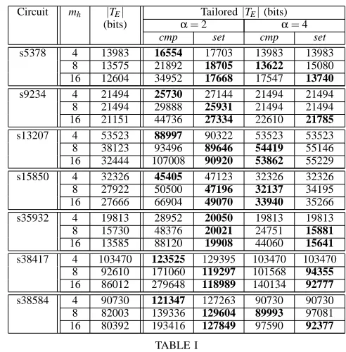
Tailoring the compressed test set: The comparison between
tailoring the compression method and tailoring the compressed test set is given in Table I. The table lists the circuit, the group size (mh),
the volume of test data (|TE|) obtained after compression, the size of
the test set after tailoring the compression method (cmp) and after tailoring the compressed test set (set), when the group size is 4, 8 and 16. Tailoring the compression method and the compressed test set has been performed for frequency ratios equal to 2 (α=2) and 4 (α=4). The best result obtained by the methods for each core, group size and frequency ratio, are marked with bold in the table. As illustrated in Section III-A, tailoring the compression method will
Circuit mh |TE| Tailored|TE|(bits)
(bits) α=2 α=4
cmp set cmp set
s5378 4 13983 16554 17703 13983 13983
8 13575 21892 18705 13622 15080
16 12604 34952 17668 17547 13740
s9234 4 21494 25730 27144 21494 21494
8 21494 29888 25931 21494 21494
16 21151 44736 27334 22610 21785
s13207 4 53523 88997 90322 53523 53523
8 38123 93496 89646 54419 55146
16 32444 107008 90920 53862 55229
s15850 4 32326 45405 47123 32326 32326
8 27922 50500 47196 32137 34195
16 27666 66904 49070 33940 35266
s35932 4 19813 28952 20050 19813 19813
8 15730 48376 20021 24751 15881
16 13585 88120 19908 44060 15641 s38417 4 103470 123525 129395 103470 103470
8 92610 171060 119297 101568 94355 16 86012 279648 118989 140134 92777 s38584 4 90730 121347 127263 90730 90730 8 82003 139336 129604 89993 97081 16 80392 193416 127849 97590 92377
TABLE I
TAILORING COMPRESSION METHOD(cmpBASED ON[13])VS.TAILORING COMPRESSED TEST SET(setSEESECTIONIII-A)
min=273854 Method Tailored|TC|(bits) % overhead
α=2 α=4 α=2 α=4
cmp 450510 332150 39.21 17.55 set 446528 320231 38.67 14.48
distr 293851 279837 6.80 2.13
TABLE II
COMPARISON WITH PREVIOUS WORK FORS1
lead to large test sets especially when the ratio between mh and α
is large. For example, in the case of s35932 for mh=16 andα=2,
tailoring the compressed test set (column 5) will lead to a reduction of 77% when compared to tailoring the compression method (column 4). Similarly, forα=4 and mh=16 a 64% reduction is obtained, when
the two methods are compared. While there are cases when tailoring the compression method leads to smaller test sets than tailoring the test set, the difference is on average of less than 5%.
Distribution architecture: The usage of the distribution
ar-chitecture (distr) is illustrated next. Two experimental setups are considered: system S1 comprising all the circuits from Table I and S2 comprising 2x s5378, 2x s9234, 2x s13207 and 2x s38584. The first system (S1) has been chosen to illustrate the potential of the proposed distribution architecture to provide test data to all the cores in a SOC and to illustrate the trade-off reduction between the VTD and synchronization overhead introduced by tailoring the compression method cmp and tailoring the compressed test set set. The second system (S2) has been chosen to illustrate the scalability of the proposed distribution architecture when compared to the interleaving architecture from [12, 17]. Both systems are tested using one ATE channel, with frequency ratios of α=2 andα=4. The results for system S1 and S2 are presented in Table II and III, respectively.
min=293182 Method Tailored|TC|(bits) % overhead
α=2 α=4 α=2 α=4
inter [12] 483162 39.32
[image:9.612.84.267.52.111.2]distr 310105 302337 5.45 3.02
TABLE III
COMPARISON WITH PREVIOUS WORK FORS2
and the synchronization overhead eliminated. For example, for core s5378, for α=2, cmp=16554 and set=17668. As also noted in Section III-A, cmp and set bring forth a trade-off between reducing the synchronization overhead and VTD. Therefore, the minimum test set for S1, when one core at the time is tested (min), and the increase in VTD, are also illustrated in Table II. The minimum test set has been computed by summing up the minimum|TE|from Table I column 3,
e.g., for core s5378 the chosen test set size has been 12604. For distr, the compressed test set obtained using a group size of 16 has been chosen for each core. It can be observed from Table II that in order to test S1, one core at a time and reduce the synchronization overhead, tailoring the compression method (cmp) obtains larger test sets than tailoring the compressed test set (set). For example, set obtains a 3% reduction over cmp for α=4. The trade-off between the VTD and synchronization overhead becomes obvious when the values obtained for cmp and set are compared to the min value. For example, there is 39% and 38% increase in VTD when cmp and set are compared to min for α=2. However, employing the distribution architecture (distr) the VTD can be reduced. For example, forα=2, 34.77% and 34.19% reductions are obtained when compared to the cmp and set approaches. Similarly, forα=4, reductions of 15.74% and 12.61% are obtained when compared to the cmp and set approaches. Note that, the sizes of the composite test sets used in conjunction with the distribution architecture are only 6.80% and 2.13% larger than
min for the circuits in S1 for α=2 and α=4 respectively. Thus, employing the distribution architecture there is virtually no trade-off between reducing the synchronization overhead and the VTD. Since the entire system can be connected to the distribution architecture without any restrictions, the proposed solution can easily fit into a design and test flow without any further modifications to the test and interface equipment, e.g. ATE or DIB. Moreover, as illustrated in Figure 10 (see Section III-B), the architecture is driven using only one data input. Hence, the distribution architecture provides an easy integration to the IEEE 1149.1 standard [22] for test data compressed SOC testing. In addition, as will be seen in Section V, the distribution unit and the decoders for the corresponding cores can be considered as a separate core which is plugged into the system.
The second experiment is detailed next. As noted in Section II-B, the interleaving architecture proposed in [12, 17] imposes certain constraints on how the cores are connected to the system, i.e., all the cores’ test sets must be compressed with Golomb using the same group size, the number of the decoders driven by the architecture is restricted to the group size and the length of the test sets for each decoder should be approximately equal. To conform with these requirements and to illustrate the scalability of the proposed distribution architecture, a group size of 4 has been considered for the interleaving architecture. Hence, the architecture drives 4 decoders of group size 4. The assignment of the cores to decoders is as follows: 2x s5378 and 2x s9234 to one decoder, 2x s13207 to the second decoder, 1x s38584 to the third decoder and the 1x s38584 to the forth decoder. This is done to obtain approximately equal length test sets for each decoder. For the distribution architecture a group size of 16 has been used for all the cores. It is important
to note that this experiment shows the scalability of the proposed approach and the benefits derived from it. Also note that when the same compression ratio is obtained by both Golomb and VIHC, and when all the requirements are fulfilled both, the interleaving architecture and the distribution architecture will yield the same TAT. Since, the interleaving architecture [12, 17] is based on the serial Golomb decoder, it does not exploit the frequency ratio. Hence, the size of the composite test set does not change with the frequency ratio. As illustrated in the table, the distribution architecture (distr) yields smaller test sets than the interleaving architecture (inter). For example, reductions of 35.81% and 37.42% in VTD are obtained for
α=2 andα=4. Hence, when cores come with different decoders and different group sizes, the proposed distribution architecture does not require any decoder’s modifications to fully exploiting them. This is contrary to the interleaving architecture which requires that the same group size is used for all the cores, and that the compressed test sets are combined to yield almost equal test sets per decoder.
Therefore, in addition to the features which allow an easy design flow integration, the proposed distribution architecture also reduces volume of test data when compared to previous methods for syn-chronization overhead reduction. Moreover, because when no the synchronization overhead is induced the VTD in bits equals the TAT in ATE clock cycles, the reduction in VTD equals the reduction in TAT. Furthermore, at-speed structural test can be facilitated by using on-chip test controllers without some of the drawbacks of the slow-fast clock approach [23], as illustrated next.
V. IMPLEMENTATION ISSUES
In this section we consider practical implementation issues related to the proposed architecture when testing core based SOCs. Our design aimed at facilitating: (a) IEEE 1149.1 compatibility, by ensuring that extending the test access port (TAP) controller [22] with one instruction will suffice for using the approach proposed in Section III; (b) stuck-at and delay fault test, hence allowing the system integrator to target different types of faults using the distribution architecture; and (c) seamless integration, through plug-and-play and easy configuration.
Test controller: As the distribution architecture generates data at
a different frequency than it receives, controlling test deployment and application from the ATE becomes very difficult. Therefore, in order to endorse (a) and (b) pointed out above, we enhance each decoder with a test controller. In addition, to support plug-and-play and easy configuration (c), each test controller has a configuration register. A high level view of the test controller is given in Figure 11(a). The inputs to the controller are prog_data_in and do_prog - for loading the configuration register, tm the test mode signal, en -to enable the decoder (see Section III-B), din - data input -to the decoder, and clks - the clocks (clk and FSM clk in Section III-B); the outputs are prog_data_out, ate_sync - for feeding in the distribution unit, se - scan enable, si - scan in data, and clk - clock. The test controller has three modes of operation: (i) test mode, when tm is high; (ii) normal mode, when tm is low, and (iii) program mode, when
do_prog is high. When in (i) test mode, it will (1) ensure that the
decoder is receiving the correct clocks, depending on the en signal;
(2) generate the scan enable se corresponding to test data shifting
(se=0) and test application (se=1) depending on the value of the
counter; (3) and generate a scan clock derived from the decoder’s
output. When in (ii) normal mode, the decoder is disabled, se is high and the generated clock is the on-chip test clock. When in (iii) program mode prog_data_in will feed the configuration register in the test controller.
en prog_data_in
do_prog
din clks
clk si se ate_sync
dout ate_sync scan_clk is_zero reload
do_prog
prog_data_out
counter conf. register
control unit
decoder
tm
clks
test type
(a) Per-decoder test controller
Ctrl. Unit Conf. Reg
Decoder Test Ctrl 1
Ctrl. Unit Conf. Reg
Decoder Test Ctrl 2 do_prog din
enable
Distribution Unit Conf. Reg
se[1..2] si[1..2] clk[1..2] prog_data_out prog_data_in
do_prog din
tm
en[1..2]
ate_sync[1..2]
[image:10.612.50.298.61.328.2](b) Distribution unit and test controller
Fig. 11. Test control
and delay-fault test, respectively) and the length of the wrapper scan chain [24] (we assume a serial core wrapper design configuration). A distribution architecture connected to two test controllers is illustrated in Figure 11(b). The configuration registers of the distribution archi-tecture and ones of the two test controllers construct a scan chain which is programmed using do_prog and prog_data_in. Thus, the entire architecture can be easily configured.
The design illustrated above can be easily connected to a TAP controller, which will control enable, do_prog and tm, of the distribution architecture, by means of one miscellaneous register (user register). In addition, since the on-chip test controller ensures clock generation at on-chip frequencies, the proposed distribution architecture represents a Load Slow/Run Fast environment which is very suitable for DFT-focused test [23]. Thus, we can achieve at-speed structural test without some of the drawbacks of using a typical slow-fast clock approach, such as using programmable PLLs for generating the launch and capture clocking [23]. It should also be noted that the TAP controller will require to only shift data, the update and capture states are not used for internal test with the proposed architecture. For issues related to at-speed structural test the interested reader is referred to [25, 26].
For the design given in Figure 11(b), we considered the decoders with a group size of 16; and we assumed the two cores with scan chains of length 256, hence, the length of the counter is 8, while the configuration register’s length is 10. The above design has been implemented using Synopsys Design Compiler [27], the synthesized design has been placed and routed using Silicon Ensemble from Cadence [28], for Alcatel 0.5µ technology library (MTC35000). At all stages, the design has been simulated using Model-Sim from Mentor Graphics [29]. The design has an area of 416982.5µm2 (≈2000· 2-input NAND gates), of which 93.00% represents the area of the two test controllers. Hence, while the distribution architecture can handle
any number of decoders, a system integrator may want to limit these in order to contain area overhead.
Test preparation: As an on-chip test set deployment and
ap-plication architecture, with data fed to the cores at a frequency different than the ATE’s, providing test application support from the ATE becomes difficult. Therefore, the test generation process, which occurs on-chip, should account for the test application as well. As noted in the beginning of Section V, we are considering stuck-at as well as delay fault tests. For delay fault tests we chose a double-capture scenario.
The test controller detailed above will ensure proper test appli-cation, however care must be taken to ensure that there is no useful test data generated by the decoder during test application. This can be achieved by either (i) modifying the uncompressed test set, depending on the type of test performed, or by (ii) ensuring that the decoder does not generate any data. For the former, each test vector is padded with one bit in the case of a stuck-at fault test, or with two bits, in the case of a double capture delay fault test. These bits will be then ignored, and not fed into the scan chain. In the case of the latter, during the test application period, the decoder’s clock will be gated. While the difference between the two cases does not appear significant, the following should be considered. In the former case (i), the test stimuli for each core must be pre-processed before compression (i.e., each test vector must be padded with 1 or 2 bits), and then the flow illustrated in Section III-B performed. In the latter case (ii), the composite test set generation illustrated in Section III-B must be altered, to consider the type of test. In our implementation we opted for solution (i).
Plug-and-play: To enable easy integration with existing designs,
the implementation should support different configurations, which will allow for various trade-off scenarios. Clearly, the distribution architecture as illustrated in Section III-B, allows for multiple core test, when for each core one decoder is chosen, or when multiple cores are connected in series. However, due to routing overhead, scan power dissipation or decoder area overhead, for example, different configurations may be desired. One scenario that can extend the proposed approach, is to feed multiple cores using the output of one test controller. Feeding multiple cores using one data input can be achieved by using a programmable clock distribution network (CDN), i.e., a shift register, which holds the configuration for the active core, and a decoder that passes the corresponding clock. Extending the test controller with such a unit, implies the connection of prog_data_out to the shift register’s input of the CDN. Note that this extension does not require any modification to the distribution architecture or test controllers. Also note that, as long as the test controllers use the same interface, adding test controllers to the distribution architecture is only limited by the number of outputs of the distribution architecture, no other modifications are required.
Finally, we illustrate a simulation screen shot obtained by simulat-ing the placed and routed design, pointsimulat-ing out the different features of the proposed approach. For demonstration purposes we considered two cores, core0 and core1, with 7 and 9 scan cells respectively. We considered for core0a single clock cycle capture test, while for core1 a double capture test. Also, the two cores use a clock period of 20ns, and the ATE clock period is of 60ns. Figure 12 illustrates one test scenario, when both cores are tested in parallel, each with its own test strategy. The figure illustrates the design immediately after it has been configured (i.e., do_prog is set low, and enable is set high). Hence,
din is fed to the decoders, and their corresponding test controllers will
1500 ns 2 us 2500 ns 3 us 3500 ns 4 us 4500 ns 5 us 3661 ns
1741 ns
1920 ns reset
ate_clk sys_clk
Single capture
Finished generating data
Double capture Enable high
Reprogram architecture
Enable low
fsm_clk do_prog
din tm enable se[0]
si[0] clk[0] se[1] si[1]
[image:11.612.103.508.48.252.2]clk[1]
Fig. 12. Simulation snapshot
or another configuration needs to be loaded, enable is set low (as marked in the figure), and the architecture reprogrammed. Note that this may occur only after all decoders have finished generating data.
VI. CONCLUSION
This paper has analyzed synchronization overhead in SOC test for coding schemes based compression methods. A two step solution for addressing the synchronization overhead problem has been proposed, which exploits frequency ratio and does not require any extra control from the ATE. The two steps, tailoring the compressed test set and the distribution architecture, add scalability and programmability features to the solution. Therefore, the proposed solution facilitates multiple core SOC test and easy integration in the design flow without imposing any restrictions on the system integrator. Additionally, detailed hardware implementation issues including the test controller and test set preparation have been considered in the paper. Hence, this paper has shown how a new test methodology based on test data compression using coding schemes, can be employed in a reduce pin count test – IEEE 1149.1 compliant environment, and also ensure stuck-at and delay fault tests.
REFERENCES
[1] ITRS, “The International Technology Roadmap for Semiconductors, 2001 Edition,” http://public.itrs.net/.
[2] A. Khoche and J. Rivoir, “I/O Bandwidth Bottleneck for Test: Is it Real ?” in Proceedings of Test Resource Partitioning Workshop. Washington, DC: IEEE Computer Society Press, Nov. 2000, pp. 2.3–1–2.3–6. [3] J. Bedsole, R. Raina, A. Crouch, and M. S. Abadir, “Very Low
Cost Testers: Opportunities and Challenges,” IEEE Design & Test of Computers, vol. 18, no. 5, pp. 60–69, Sept. 2001.
[4] J. Rajski, J. Tyszer, M. Kassab, N. Mukherjee, R. Thompson, K.-H. Tsai, A. Hertwig, N. Tamarapalli, G. Mrugalski, G. Eide, and J. Qian, “Embedded Deterministic Test for Low Cost Manufacturing Test,” in Proceedings IEEE International Test Conference (ITC). Baltimore, MD: IEEE Computer Society Press, Oct. 2002, pp. 301–310.
[5] P. T. Gonciari, B. Al-Hashimi, and N. Nicolici, “Integrated Test Data Decompression and Core Wrapper Design for Low-Cost System-on-a-Chip Testing,” in Proceedings IEEE International Test Conference (ITC). Baltimore, MD: IEEE Computer Society Press, Oct. 2002, pp. 64–73. [6] ——, “Variable-length Input Huffman Coding for System-on-a-Chip
Test,” IEEE Transactions on Computer-Aided Design, vol. 22, pp. 783– 796, June 2003.
[7] T. Warwick, “What a Device Interface Board Really Costs: An Evalya-tion of Technical ConsideraEvalya-tions for Testing Products Operating in the Gigabit Region,” in Proceedings IEEE International Test Conference
(ITC). Baltimore, MD: IEEE Computer Society Press, Oct. 2002, pp.
555–564.
[8] D. McFeely, “The Process and Chanllenges of a High-Speed DUT Board Project,” in Proceedings IEEE International Test Conference (ITC). Baltimore, MD: IEEE Computer Society Press, Oct. 2002, pp. 565–573. [9] B. Koenemann, C. Barnhart, B. Keller, T. Snethen, O. Farnsworth, and D. Wheater, “A SmartBIST Variat with Guaranteed Encoding,” in
Proceedings of the Asian Test Symposium (ATS). Kyoto, Japan: IEEE
Computer Society Press, Nov. 2001, pp. 325–330.
[10] I. Bayraktaroglu and A. Orailoglu, “Test Volume and Application Time Reduction Through Scan Chain Concealment,” in Proceedings ACM/IEEE Design Automation Conference (DAC), vol. 38, June 2001, pp. 151–155.
[11] E. H. Volkerink, A. Khoche, and S. Mitra, “Packet-Based Input Test Data Compression Techniques,” in Proceedings IEEE International Test
Conference (ITC). IEEE Computer Society Press, Oct. 2002, pp. 154–
163.
[12] A. Chandra and K. Chakrabarty, “System-on-a-Chip Test Data Com-pression and DecomCom-pression Architectures Based on Golomb Codes,” IEEE Transactions on Computer-Aided Design, vol. 20, pp. 113–120, Mar. 2001.
[13] A. Jas, J. Ghosh-Dastidar, M.-E. Ng, and N. A. Touba, “An efficient test vector compression scheme using selective Huffman coding,” IEEE Transactions on Computer-Aided Design, vol. 22, pp. 797–806, June 2003.
[14] L. Li and K. Chakrabarty, “Test Data Compression Using Dictionaries with Fixed-Length Indices,” in Proceedings IEEE VLSI Test Symposium
(VTS). IEEE Computer Society Press, Apr. 2003, pp. 219–224.
[15] V. D. Agrawal and T. J. Chakraborty, “High-Performance Circuit Test-ing with Slow-Speed Testers,” in ProceedTest-ings IEEE International Test
Conference (ITC). Montreal, Canada: IEEE Computer Society Press,
Apr. 1995, pp. 302–310.
[16] D. Heidel, S. Dhong, P. Hofstee, M. Immediato, K. Nowka, J. Silberman, and K. Stawiasz, “High-speed serialiazing/deserializing design-for-test methods for evaluating a 1 ghz microprocessor,” in Proceedings IEEE VLSI Test Symposium (VTS). IEEE Computer Society Press, Apr. 1998, pp. 234–238.
[17] A. Chandra and K. Chakrabarty, “Test Resource Partitioning for SOCs,” IEEE Design & Test of Computers, vol. 18, no. 5, pp. 80–91, Sept. 2001. [18] ——, “Frequency-Directed Run-Length (FDR) Codes with Application to System-on-a-Chip Test Data Compression,” in Proceedings IEEE VLSI Test Symposium (VTS). IEEE Computer Society Press, Apr. 2001, pp. 114–121.
[19] ——, “Test Resource Partitioning and Reduced Pin-Count Testing Based on Test Data Compression,” in Proceedings Design, Automation, and
Test in Europe (DATE). IEEE Computer Society Press, Mar. 2002, pp.
[20] The University of Illinois, www.crhc.uiuc.edu/IGATE.
[21] F. Brglez, D. Bryan, and K. Kozminski, “Combinational profiles of sequential benchmark circuits,” in Proceedings International Symposium on Circuits and Systems (ISCAS), May 1989, pp. 1929–1934. [22] M. Abramovici, M. A. Breuer, and A. D. Friedman, Digital Systems
Testing and Testable Design. IEEE Press, 1990.
[23] K. Posse and G. Eide, “Key Impediments to DFT-Focused Test and How to Overcome Them,” in Proceedings IEEE International Test Conference
(ITC). Charlotte, NC: IEEE Computer Society Press, Oct. 2003, pp.
503–511.
[24] E. J. Marinissen, R. Kapur, and Y. Zorian, “On Using IEEE P1500 SECT for Test Plug-n-Play,” in Proceedings IEEE International Test
Conference (ITC). Atlantic City, NJ: IEEE Computer Society Press,
Oct. 2000, pp. 770–777.
[25] X. Lin, R. Press, J. Rajski, P. Reuter, T. Rinderknecht, B. Swanson, and N. Tamarapalli, “High-Frequency, At-Speed Scan Testing,” IEEE Design & Test of Computers, vol. 20, no. 5, pp. 17–25, Sept. 2003.
[26] S. Pateras, “Achieving At-Speed Structural Test,” IEEE Design & Test of Computers, vol. 20, no. 5, pp. 26–32, Sept. 2003.
[27] Synopsys Inc., “Design Compiler,” http://www.synopsys.com/, 2003. [28] Cadence Design Systems Inc., “Silicon Ensemble,”
http://www.cadence.com/, 2003.
[29] Model Technology Inc., “ModelSim, HDL Simulator,” http://www.model.com/, 2002.
Paul Theo Gonciari (S’02 - M’04) received the Dipl Ing degree in computer engineering from the University of Timisoara, Romania, 1999 and the PhD degree in electronics and computer science from the University of Southampton, United Kingdom, 2003.
He is a Research Fellow in the Electronics and Computer Science School at the University of Southampton. His current research interests are in the area of computer-aided design and test, with emphasis on low-cost core based system-on-a-chip test, in particular on test resource partitioning and optimization. He is a member of the ACM SIGDA and the IEEE Computer and Circuits and Systems Societies.
Bashir M. Al-Hashimi (M’ 99-SM’ 01) received the B.Sc. degree with 1st-class classification in Electri-cal and Electronics Engineering from the University of Bath, UK, in 1984, and the Ph.D. degree from York University, UK, in 1989. Following this he worked in industry for six years designing high performance chips for analog and digital signal processing applications, developing CAD tools for simulation and synthesis of analogue and digital circuits. In 1995, he joined Staffordshire University, UK, where he formed the VLSI Signal Processing research group with funding from industry and government. In 1999, he joined the Department of Electronics and Computer Science, Southampton Univer-sity, UK, where he is currently a Professor of Computer Engineering. He has authored one book on SPICE simulation, (CRC Press,1995), and coauthored two books, “Power Constrained Testing of VLSI circuits” (Kluwer Academic, 2002), and “System-Level Design Techniques for Energy-Efficient Embedded Systems” (Kluwer Academic, 2004). He has authored and coauthored over 125 technical papers. His research and teaching interests include low-power hardware-software co-design, System-on-chip test, and VLSI CAD.
Dr Al-Hashimi is the Editor-in-Chief of the IEE Proceedings: Computers and Digital Techniques, and a Member of the Editorial Board of the Embedded Computing Journal. He has served on the IEEE/ACM Design Automation and Test in Europe (DATE) conference in various capacities including Topic Chair (Simulation and Emulation, 2001-2004), and for 2005 as a Member of the Executive Committee as Chair for FridayWorkshops. He is a Member of the Technical Program Committee of the IEEE European Test Symposium and the IEEE VLSI Test Symposium. He has served as the Guest Editor for a number of journal special issues; the most recent are “UK Embedded System Design”, (Design Automation for Embedded Systems Journal, Kluwer, 2002), and “Low Power SoC”, (IEE Proceedings: Computers and Digital Techniques, 2002). Dr Al-Hashimi was the co-author of a Best Paper Award at the 2000 IEEE International Test Conference relating to low power BIST for RTL data paths.
![Fig. 6.Interleaving architecture based on [12]](https://thumb-us.123doks.com/thumbv2/123dok_us/8509774.349780/4.612.303.558.72.328/fig-interleaving-architecture-based-on.webp)
![TABLE IIIarchitecture and the distribution architecture will yield the same TAT.Since, the interleaving architecture [12, 17] is based on the serialOMPARISON WITH PREVIOUS WORK FOR S2Golomb decoder, it does not exploit the frequency ratio](https://thumb-us.123doks.com/thumbv2/123dok_us/8509774.349780/9.612.84.267.52.111/iiiarchitecture-distribution-architecture-interleaving-architecture-serialomparison-previous-frequency.webp)