Article
A Zero Bias Pixel Sensor and its Zero-Bias Column
Buffer-Direct-Injection Circuit
Pusit Suriyavejwongs
a,*
, Ekachai Leelarasmee
b, and Wanchalerm Pora
cDepartment of Electrical Engineering, Faculty of Engineering, Chulalongkorn University, Thailand E-mail: a[email protected] (Corresponding author), b[email protected], c[email protected]
Abstract. Two pixel sensors, namely active pixel sensor (APS) and pseudo-active pixel sensor (PAPS), are reviewed to show that APS suffers from dark current while PAPS suffers from leakage current. Then a new pixel sensor called zero bias pixel sensor (ZBPS) in which only two MOS switches in addition to the photodiode are used, one for connecting the pixel’s photodiode to a column bus and the other for bypassing it. A zero-bias column buffer-direct-injection (ZCBDI) circuit, which is similar to a regulated cascode amplifier, is used to control the voltage at column bus at zero. All ZBPS pixels are guaranteed to work at zero voltage at all times to eliminate the dark current as well as leakage current. A case of a 10µm x 10µm ZBPS pixel designed with standard 0.18µm CMOS process is studied through simulation. This pixel generates a photocurrent within a range from 1pA to 100nA. To handle a large variation of photocurrent while maintaining zero column voltage, the ZCBDI is designed using differential cascode, common source, and buffer stages and then compensated for 50 degree phase margin. Transient simulation shows that the pixel steady state response time is around 1.406ms, leading to at most 5.5 frames per second for an image of 128x128 ZBPS pixels. The fill factor of ZBPS for this case is around 59%.
Keywords: CMOS sensor, zero bias pixel, dark current.
ENGINEERING JOURNAL Volume 21 Issue 5 Received 24 January 2017
1.
Introduction
A CMOS image sensor as shown in Fig. 1(a) is a device that converts light from an object into electrical signal so that its image can be captured and stored in digital form. It is found in many consumer products such as digital camera, smart phone, and medical imaging equipment [1-4]. The general structure of a CMOS image sensor is shown in Fig. 1(b) where a major portion of the chip area is occupied by an array of pixels. All pixels in the same column share their output and all pixels in each row are selected by activating a row select control which connects them to their respective column readout for further processing. A pixel consists of a photodiode, a select switch and other interface (if any) as shown in Fig. 1(c). For maximum sensitivity [5, 6], the photodiode should occupy the largest proportion of the total pixel area or “fill factor”. With today advance technology, it is common to find a CMOS image sensor having as array of 1,000x1,000 or 1 million pixels, each of which has a size less than 10µm x 10µm.
Fig. 1. (a) CMOS image sensor [7]; (b) array of pixels; (c) pixel structure.
Fig. 2 shows the symbol of a photodiode and its characteristic curves. Physically, a photodiode consists of a junction of p and n type semiconductor layers[8]. When exposed to light, electron-hole pairs are generated in the junction’s space charge region and driven out by the electric field from the applied bias voltage Vph, generating a photocurrent Ip that is proportional to the light intensity P and the bias voltage. At
the same time, the bias voltage Vph also causes an additional current, called “dark current” or Idark, due to
tunneling and SRH generation [9, 10]. Therefore the output current Iph of the photodiode is the sum of
photocurrent Ip and dark current Idark. Note that dark current disappears when the photodiode is operated
at zero voltage.
[image:2.595.77.501.239.466.2] [image:2.595.129.458.613.750.2]This paper focuses on a pixel structure that produces low dark current since it not only degrades optical dynamic range, but also contributes noise[9, 11, 12].In particular, 2 types of pixel structure are reviewed. They are active pixel sensor (APS) [6, 13-25] in Section 2 and pseudo-active pixel sensor (PAPS) [26, 27] in Section 3. Then a new sensor called zero bias pixel sensor (ZBPS), that can eliminate dark current, is proposed in Section 4. Since ZBPS requires a zero-bias column buffer-direct-injection (ZCBDI) circuit to control the column bus at zero voltage, a design case of ZCBDI capable of supporting 1pA to 100nA of photocurrent is described in Section 5. Section 6 finishes the design with frequency compensation for stability along with transient simulation studied in Section 7 which characterizes the achieved frame rate. Conclusion is then discussed in Section 8.
2.
Active Pixel Sensor (APS)
The most common CMOS pixel sensor is the active pixel sensor (APS) [6, 13-25] which has 2 conventional types, namely 3T APS [6, 14, 18, 21-24] and 4T APS [13-20, 25], as shown in Fig. 3. Both types use the junction capacitor of a photodiode to integrate its current and measure the change in its voltage after a fixed time interval which depends linearly on the incident light intensity. The 3T APS uses 3 MOS transistors and can be fabricated in a standard low cost CMOS process but suffers from dark current and reset noises [9, 11, 12]. The more popular 4T APS uses 4 MOS transistors and replaces the photodiode with a “pinned” photodiode [13] which inherently has lower dark current but requires special fabrication steps. The fill factor is usually around 40% for 3T APS and 30% for 4T APS.
Fig. 3. (a) 3T active pixel sensor; (b) 4T active pixel sensor.
The light conversion of 3T APS is described with the help of Fig. 4 as follows. First, a pixel is reset, as seen in Fig. 4(a), so that its junction capacitor Cj is charged by the DC supply VDD. Then the reset switch is
off and the pixel capacitor is discharged by its photocurrent and dark current, as seen in Fig. 4(b), causing its voltage to ramp down, i.e.
0
1
( ) - ( )( )
t
ph DD p dark
j
V t V I I t dt
C (1).
At the end of the integration time T, typically in the order of milliseconds, the voltage of the selected pixel is readout by the buffer to the column bus as depicted in Fig. 4(c). Then the pixel goes back to a new cycle. Note that APS pixel cannot reduce or eliminate dark current, although 4T APS replaces the normal photodiode by a pinned photodiode which has lower dark current [28].
3.
Pseudo-Active Pixel Sensor (PAPS)
[image:3.595.138.462.343.456.2]shared by all pixels in the same column. It consists of an operational amplifier for zero biasing and a buffer PMOS or NMOS for injecting the photocurrent to charge a column capacitor Cint which was initially
discharged (Fig. 5 left) by the reset switch. After a fixed integration time T, the capacitor voltage is readout and is given by
int int
int 0
1
( ) ( )
T
V T I t dt
C (2)
Note that the column bus is hold by ZCBDI at VDD for the left PAPS and zero for the right PAPS.
Since a PAPS needs only one select switch, its fill factor can be high. For example, the fill factor of a 5.8µm x 5.8µm PAPS pixel size can reach 58%.
Fig. 4. Operation of 3T APS during (a) reset, (b) integration and (c) readout phase.
Fig. 5. PAPS using p+/n-well (left) and n-well/p-substrate (right) photodiodes.
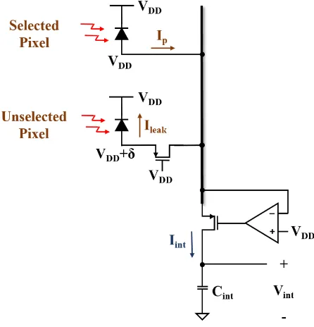
Since any unselected PAPS pixel is not connected to the column bus, its photocurrent causes a forward self bias voltage δ (see Fig. 6) of a few hundred millivolt. This voltage can produce a leakage current Ileak through its own select switch to the column bus as shown in Fig. 6. Therefore the current Iint
[image:4.595.84.523.240.355.2] [image:4.595.109.484.390.662.2]connected to a column. In [27], it is suggested that one ZCBDI should be shared with only 4 PAPS pixels, called OPAPS. This results is using more than one ZCBDI per column and effectively reduces the fill factor down to 42% for a 352x288 pixel array. Also since the photocurrent decreases with the reverse bias voltage, its value is smaller than that of APS.
Fig. 6. Operation of PAPS during integration.
4.
Zero Bias Pixel Sensor (ZBPS)
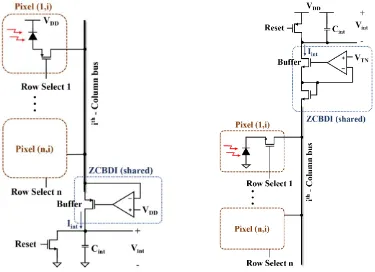
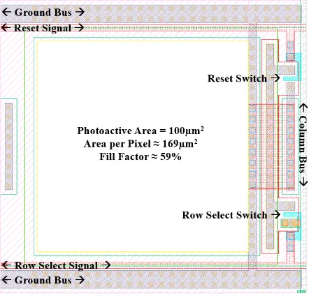
To eliminate leakage currents from unselected PAPS pixels, a bypass switch is added across each photodiode as shown in Fig. 7(a). In this new structure, a selected pixel is zero biased by ZCBDI while unselected pixels are bypassed as shown in Fig. 7(b). Using this technique, all pixels are always be zero biased and the pixel sensor is thus called “zero bias pixel sensor” or ZBPS. With no leakage, there is no limit on the number of pixels connected to a column which is an advantage over PAPS. Note also that there is a slight difference in designing ZCBDI between ZBPS (Fig. 7) and PAPS (Fig. 5). The disadvantage of ZBPS is that its fill factor tends to lower than PAPS. As an example, a 10µmx10µm ZBPS design is shown in Fig. 8. Its fill factor is 59% which is comparable of PAPS in [26] (with pixel size almost 4 times bigger) but larger than 42% of OPAPS in [27].
5.
A Circuit Design of a ZCBDI
Designing ZCBDI is challenging because it has to handle photocurrent of 5 order of magnitude variation. Also there is a stability issue with the circuit since it employs a feedback loop to control the column at zero voltage. Here we present a design case where a pixel generates 1pA at low light condition and 100nA at full light intensity. Its size is 10µm x 10µm, using 0.18µm CMOS process with the following parameters.
Electron mobility factor µnCOX = 200µA/V2
Threshold voltage VTH = 0.47V
p-n saturation current IS = 210aA
Minimum width Wmin = 0.22µm
Minimum length Lmin = 0.18µm
[image:5.595.186.409.146.378.2]Fig. 7. (a) ZBPS structure; (b) Operation of selected and unselected ZBPS.
Fig. 8. Layout of a 10µm x 10µm ZBPS.
It is clear from Fig. 7 that the gain of the operational amplifier, A, should be large to make the bias voltage, Vph, approach zero. Sincethe operational amplifier drives the gate of the buffer, its output voltage,
Vop, should have a high swing to enable the buffer to carry a large variation of photocurrent from 1pA to
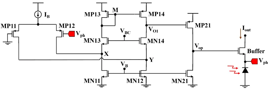
100nA. With these observations, the operational amplifier is designed to have two cascaded stages as shown in Fig. 9. The first stage is a high gain folded cascode amplifier [29] and consists of MN11-MN14 and MP11-MP14. The second stage, consisting of MN21 and MP21, is a common source amplifier with a high swing for driving the buffer. Analytically, the gain of the folded cascade amplifier is
' '12 14
cascode mp op
A
g
r
(3)
' 12
12 12 12
12 1/ 13
on
mp mp mp
on mn
R
g g g
R g (4)
'
14 14
(
12 14 14)
14op op op mn on op
[image:6.595.116.477.79.305.2] [image:6.595.187.408.342.554.2] [image:6.595.220.405.694.768.2]where gmx, rox are transconductance and output resistance of Mx transistor respectively.
Similarly the gain of the common source amplifier is
21(
21 21)
c source mp op on
A
g
r
r
(6)The total gain is A=Acascode x Ac-source. Note that the valuesofgmx, rox depend not only on MOS sizes but
also on the DC operating point which, in turn, depends on the photocurrent. Therefore the designed circuit of Fig. 9will be verified for two extreme values of photocurrent, i.e. 1pA and 100nA. Since all MOS are of short channel type, exact formula for determining gmx, rox can only be obtained by numerical simulation.
[image:7.595.70.528.271.426.2]Thus the design procedure starts with choosing initial values of MOS size and iteratively adjusting them until the simulation result yields satisfactory results. After several iterations, the appropriate size of all MOS and DC sources are tabulated in Table 1. DC quiescent values at various photocurrents are tabulated in Table 2 which shows that the designed ZCBDI circuit can vary the amplifier output Vop wide enough the
keep the bias voltage Vph very close to zero.
Fig. 9. Schematic diagram of a ZCBDI.
Table 1. MOS sizes and biases of the ZCBDI designed in Fig. 9.
Component W/L or Value
MP11, MP12, MP13, MP14, MP21 2µm/20µm MN11, MN12, MN13, MN14 2µm/60µm
MN21 1µm/60µm
Buffer 0.22µm/120µm
IB 100nA
VBC 1.0V
VB 0.7V
Table 2. DC operating values of the designed ZCBDI at various photocurrent.
Iph Vph Vop
1pA 1.8µV 172mV 10pA 220nV 259mV 100pA 88nV 359mV 1nA 29nV 492mV 10nA -50nV 720mV 100nA -252nV 1.31V
From Table2, Vph is indeed very small as desired but turns out to be slightly negative at large
[image:7.595.184.411.626.715.2]
op0 op phV
V
V
A
(7).
where Vop0 is the output voltage at the DC condition when the two inputs of the operational amplifier are
equal to zero, therefore, Vop0 is not zero in this case. From the buffer MOS transistor, we have
(
)
ph op gs ph
V
V
V I
(8).
where Vgs is the gate source driving voltage which depends on Iph. Solving these two relations, we obtain
0 ( )
1
op gs ph
ph
V V I
V
A (9)
.
Therefore Vph goes to zero when A is large. However, Vgs increase with Iph, although nonlinearly. Thus Vph
can be negative when Iph is large, i.e. 10nA and 100nA for this design. This effect can be reduced by making
the buffer MOS bigger.
6.
Stability and Compensation of the ZCBDI Circuit
Despite having good property in keeping Vph at almost zero in steady state DC situation, the ZCBDI circuit
is susceptible to transient instability because it has a negative feedback path from the pixel to the input of the operational amplifier. Stability is determined from the phase margin obtained from the frequency response of the loop gain, Aloop, which is equal to the product of the gains of the cascode stage, output
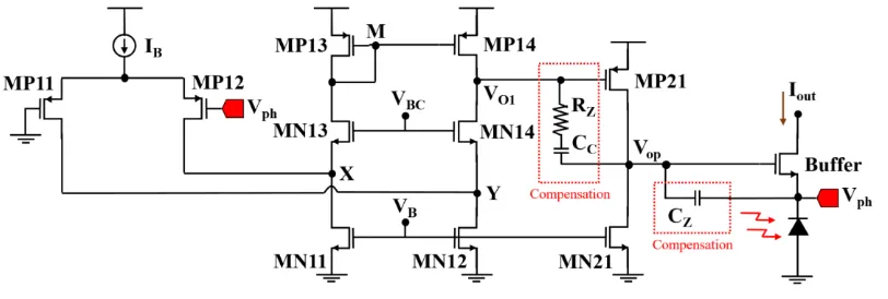
stage and current buffer stage. Due to different small signal characteristics since different quiescent point at each photocurrent value, its magnitude and phase vary with frequency. Fig. 10depicts a simulated 1mHz - 1MHz frequency response plot of the loop gain of the ZCBDI of Fig. 9 at two extreme pixel currents, i.e. 1pA and 100nA. From these graphs, the frequency at which the magnitude of the gain is 1 or fUG is found
[image:8.595.130.464.461.691.2]to be 5.94kHz and 227kHz and the phase margin at fUG is 12 and -164 degree respectively.
Fig. 10. Frequency response of the loop gain of uncompensated ZCBDI at 1pA and 100nA pixel current.
for CC is to exploit its Miller effect to lower the dominant pole of the magnitude plot which occurs at node
O1. It can be approximated to be
Dominant pole
' 14 11
(
(1
)
)
op O c source C
r
C
A
C
(10)where CO1 is the parasitic node capacitance. Other components RZ and CZ create zeroes at
21 21(
1)
mpmp Z C
g
g
R
C
(11)and
mbufferZ
g
C
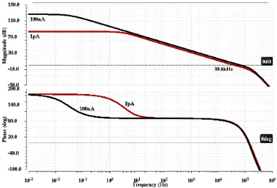
(12).These zeroes improve the phase margin by cancelling the effect of non-dominant poles. Through iterations, a good choice of these components is found to beRZ = 4.1MΩ, CC =1pF and CZ = 0.5pF. The loop
[image:9.595.97.503.345.482.2]frequency plot of this compensated ZCBDI is depicted in Fig. 12 giving 50 and 70 degree of phase margin at 1pA and 100nA photocurrent. These margins are sufficient to guarantee stability.
Fig. 11. ZCBDI using RZ, CC and CZ as compensating components.
7.
Transient Response of the Compensated ZCBDI Circuit
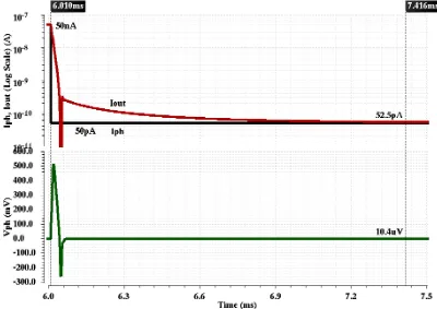
Once stabilized, the transient simulation of the compensated ZCBDI inFig. 11is carried out. Here the Iph
changes stepwise only from 50pA to 50nA corresponding to typical 50 lux to 50,000 lux ambient condition thereby yielding 10 bits of digitization resolution. Although the main function of ZCBDI is to control the pixel bias voltage at zero, it also has to accurately buffer Iph to Iout.Therefore the settling time or TS is
determined from considering on Iout (time for Iout to reach within ±5% of the steady value) instead of Vph.
Careful derivation of the small signal analysis shows that this settling time is approximately proportional to Iph, although the exact value is difficult to determine from such a large signaltransition.Fig. 13 shows the
transient waveform with Iph varies from 50pA to 50nA giving 15µs settling time, whereas Fig. 14 shows the
response of step Iph from 50nA to 50pA with a much longer settling time of 1.406ms. Note that the
waveform of Vph experience ringing behavior which indicates that the phase margin of the loop is not large
enough to suppress the ringing. Since TS is the time to process one row of pixels, the frame rate to capture
an array of Nrows x Ncolumn of pixels is then given by
Frame rate
1
rows s
N T (13)
where TS is the longest settling time. Therefore the frame rate of a 1000x1000 pixels is 0.7 frames per
Fig. 12. Frequency response of the loop gain of compensated ZCBDI.
Fig. 14. Transient response of the compensated ZCBDI for a 50nA to 50pA step of photocurrent.
8.
Conclusion
Operating a photodiode at zero voltage can completely eliminate its dark current. This has led to a new pixel called zero bias pixel sensor (ZBPS) in which all pixels are always biased at near zero voltage. A ZBPS structure requires 2 MOS transistors in addition to the photodiode, one for select and the other for bypass. The basic idea is to bypass unselected pixels while connecting the selected one to a column bus that is hold at zero voltage by a shared regulated cascode amplifier called ZCBDI. This new sensor has the lowest dark current when compared with APS and PAPS. The conceptual and detailed design of the ZCBDI for a 10µm x 10µm pixel in a 0.18µm CMOS process that is capable of handling the photocurrent with a five order of magnitude variation is described. Transient simulation of the designed circuit shows that the output current takes 1.406ms to reach the steady state value, giving rise to a maximum speed of 0.7 frames per second for a 1000x1000 pixels and 5.5 frames per second for a 128x128 pixels. This design is appropriate for taking still pictures.
Acknowledgment
The research is supported by Department of Electrical Engineering, Faculty of Engineering, Chulalongkorn University and Silicon Craft Technology Co., Ltd. The authors also wish to thank reviewers for valuable comments that help improving the quality of this work.
References
[1] K. Humphreys, C. Markham, and T. E. Ward, “A CMOS camera-based system for clinical photoplethysmographic applications,” in OPTO-Ireland, 2005, pp. 88-95.
[2] G. S. Day and P. J. Schoemaker, Peripheral Vision. Boston: Harvard Business School Press,2006. [3] H. S. Lamphar and F. Kundracik, “A microcontroller-based system for automated and continuous sky
glow measurements with the use of digital single-lens reflex cameras,” Lighting Research and Technology,
[4] R. Fontaine, “The state-of-the-art of mainstream CMOS image sensors,” in Proceedings of the International Image Sensors Workshop, 2015, pp. 6-12.
[5] T. Lule, S. Benthien, H. Keller, F. Mutze, P. Rieve, K. Seibel, M. Sommer, and M. A. B. M. Bohm, “Sensitivity of CMOS based imagers and scaling perspectives,” IEEE Transactions on Electron Devices,
vol. 47, pp. 2110-2122, 2000.
[6] B. Blanco-Filgueira, P. Lopez, D. Cabello, J. Ernst, H. Neubauer, and J. Hauer, “Modeling and simulation of CMOS APS,” in 2009 Spanish Conference on Electron Devices, 2009, pp. 120-123.
[7] Teledyne e2v. (2012). e2v Launches 1.3MP Ruby CMOS Imaging Sensors. [Online]. Available: http://www.e2v.com/news/e2v-launches-1-3mp-ruby-cmos-imaging-sensors/
[8] G. P. Weckler, “Operation of p-n junction photodetectors in a photon flux integrating mode,” IEEE Journal of Solid-State Circuits, vol. 2, pp. 65-73, 1967.
[9] B. Pain, T. Cunningham, B. Hancock, C. Wrigley, and C. Sun, “Excess noise and dark current mechanisms in CMOS imagers,” in IEEE Workshop on CCD’s and Advanced Image Sensors, Karuizawa, Nagano, Japan, 2005.
[10] T. Watanabe, J. H. Park, S. Aoyama, K. Isobe, and S. Kawahito, “Effects of negative-bias operation and optical stress on dark current in CMOS image sensors,” IEEE Transactions on Electron Devices, vol. 57, pp. 1512-1518, 2010.
[11] T. Hui, B. Fowler, and A. E. Gamal, “Analysis of temporal noise in CMOS photodiode active pixel sensor,” IEEE Journal of Solid-State Circuits, vol. 36, pp. 92-101, 2001.
[12] I. Brouk, A. Nemirovsky, and Y. Nemirovsky, “Analysis of noise in CMOS image sensor,” in 2008 IEEE International Conference on Microwaves, Communications, Antennas and Electronic Systems, 2008, pp. 1-8. [13] R. M. Guidash, T. H. Lee, P. P. K. Lee, D. H. Sackett, C. I. Drowley, M. S. Swenson, L. Arbaugh, R.
Hollstein, F. Shapiro, and S. Domer, “A 0.6 um CMOS pinned photodiode color imager technology,” in International Electron Devices Meeting. IEDM Technical Digest, 1997, pp. 927-929.
[14] A. J. P. Theuwissen, “Better pictures through physics,” IEEE Solid-State Circuits Magazine, vol. 2, pp. 22-28, 2010.
[15] S. Mendis, S. E. Kemeny, and E. R. Fossum, “CMOS active pixel image sensor,” IEEE Transactions on Electron Devices, vol. 41, pp. 452-453, 1994.
[16] S. K. Mendis, S. E. Kemeny, R. C. Gee, B. Pain, C. O. Staller, Q. Kim, and E. R. Fossum, “CMOS active pixel image sensors for highly integrated imaging systems,” IEEE Journal of Solid-State Circuits,
vol. 32, pp. 187-197, 1997.
[17] X. Wang, M. F. Snoeij, P. R. Rao, A. Mierop, and A. J. P. Theuwissen, “A CMOS image sensor with a buried-channel source follower,” in 2008 IEEE International Solid-State Circuits Conference - Digest of Technical Papers, 2008, pp. 62-595.
[18] E. R. Fossum, “CMOS image sensors: electronic camera-on-a-chip,” IEEE Transactions on Electron Devices, vol. 44, pp. 1689-1698, 1997.
[19] X. Qian, H. Yu, S. Chen, and K. S. Low, “Design and characterization of radiation-tolerant CMOS 4T Active Pixel Sensors,” in 2014 International Symposium on Integrated Circuits (ISIC), 2014, pp. 520-523. [20] F. Tang, D. G. Chen, B. Wang, and A. Bermak, “Low-power CMOS image sensor based on
column-parallel single-slope/SAR quantization scheme,” IEEE Transactions on Electron Devices, vol. 60, pp. 2561-2566, 2013.
[21] T. Wang, X. Huang, M. Yan, H. Yu, K. S. Yeo, I. Cevik, and S. Ay, “A 96x96 1V ultra-low power CMOS image sensor for biomedical application,” in 2012 IEEE Asia Pacific Conference on Circuits and Systems, 2012, pp. 13-16.
[22] S. U. Ay, “Boosted readout for CMOS APS pixels,” in 2011 IEEE International Symposium of Circuits and Systems (ISCAS), 2011, pp. 2205-2208.
[23] B. Ackland and A. Dickinson, “Camera on a chip,” in 1996 IEEE International Solid-State Circuits Conference. Digest of TEchnical Papers, ISSCC, 1996, pp. 22-25.
[24] S. U. Ay, “Electrical property modelling of photodiode type CMOS active pixel sensor (APS),” in 48th Midwest Symposium on Circuits and Systems, 2005., 2005, pp. 371-375 Vol. 1.
[25] I. Takayanagi and J. Nakamura, “High-resolution CMOS video image sensors,” in Proceedings of the IEEE, vol. 101, pp. 61-73, 2013.
[27] S. Yu-Chuan and W. Chung-Yu, “Optimal design of CMOS pseudoactive pixel sensor (PAPS) structure for low-dark-current and large-array-size imager applications,” IEEE Sensors Journal, vol. 5, pp. 956-963, 2005.
[28] D. Durini and B. J. Hosticka, “Photodetector structures for standard CMOS imaging applications,” in
![Fig. 2of a junction of p and n type semiconductor layersgenerated in the junction’s space charge region and driven out by the electric field from the applied bias voltage Vthe same time, the bias voltage Vtunneling and SRH generation [9, 10]](https://thumb-us.123doks.com/thumbv2/123dok_us/8107823.235563/2.595.129.458.613.750/junction-semiconductor-layersgenerated-junction-electric-voltage-vtunneling-generation.webp)