Little Board
™
/286
Technical Manual
P/N: 5000281
Revision: A
Ampro Computers, Incorporated
4757 Hellyer Avenue
nSan Jose, CA 95138
Tel (408) 360-0200
nFAX (408) 360-0220
NOTICE
DISCLAIMER
Ampro Computers, Incorporated makes no representations or warranties with respect to the contents of this manual or of the associated Ampro software products, and specifically disclaims any implied warranties of merchantability or fitness for any particular purpose. Ampro shall under no circumstances be liable for incidental or consequential damages or related expenses resulting from the use of this product, even if it has been notified of the possibility of such damages. Ampro reserves the right to revise this publication from time to time without obligation to notify any person of such revisions. If errors are found, please contact Ampro at the address listed on the title page of this document.
TRADEMARKS
MiniModule, MiniBackplane, Little Board, StackPlane: Ampro Computers, Inc.
AT, PC/AT, IBM: International Business Machines Corp.
DR DOS: Digital Research, Inc.
Hercules: Hercules Computer Technology
MS-DOS: Microsoft, Inc.
UNIX: AT&T Bell Laboratories
XENIX: Santa Cruz Operation, Incorporated
QNX: Quantum Software Systems, Ltd.
COPYRIGHT 1989, 1990 AMPRO COMPUTERS INCORPORATED
PREFACE
This manual is for integrators and programmers of systems based on the Ampro Little Board/286 single board system. It contains information on hardware requirements and interconnection, and details of how to program the system.
There are four chapters, organized as follows:
n Chapter 1 -- Introduction. General information pertaining to the Little Board/286,
its features, and specifications.
n Chapter 2 -- Hardware Configuration. A description of how to configure and connect the Little
Board/286 for use with a wide variety of onboard and external devices. Included are tables listing the pinouts of each of the board's connectors, board jumper and Configuration Memory setup, and considerations and specifications regarding peripheral devices.
n Chapter 3 -- Software Configuration. An overview of the system features,
configuration options, and utilities that are available under the "DOS" (PC-DOS, MS-DOS, or DR-DOS) operating system, including system setup guidelines.
n Chapter 4 -- Theory of Operation. Detailed technical information on Little
TABLE OF CONTENTS
CHAPTER 1 - INTRODUCTION
1.1 General Description ... 1-1 1.2 Little Board/286 Features... 1-3
1.3 Little Board/286 Specifications... 1-4
CHAPTER 2 - HARDWARE CONFIGURATION
2.1 Introduction ... 2-1 2.1.1 Interface Connectors ... 2-1
2.1.2 Jumper Configuration Options ... 2-3
2.1.3 "Soft Configuration" Options ... 2-3 2.2 DC Power Input... 2-4
2.3 Onboard Device Options and Configuration... 2-6
2.3.1 CPU and Bus Half-Speed Options... 2-6
2.3.2 DRAM Memory... 2-6 2.3.3 Math Coprocessor ... 2-7
2.3.4 Byte-Wide Memory Sockets... 2-8
2.3.5 Battery-Backed Clock... 2-10
2.4 Peripheral Connections and Configuration ... 2-12
2.4.1 Utility Connector ... 2-12 2.4.2 Keyboard... 2-13 2.4.3 Parallel Printer Port... 2-14 2.4.4 Serial Ports... 2-16 2.4.5 Floppy Disk Interface ... 2-17 2.5 SCSI Interface ... 2-20 2.5.1 Normal Use of SCSI ... 2-21
2.5.2 The Ampro SCSI/BIOS ... 2-21
2.5.3 Simple Bidirectional I/O... 2-22
2.5.4 SCSI Interface Configuration ... 2-22
2.6 AT Expansion Bus ... 2-24
2.6.1 Onboard MiniModule Header and Bus Expansion... 2-24
2.6.2 Using Standard PC and AT Bus Cards ... 2-25
2.6.3 Expansion Bus Cable Considerations... 2-26
2.6.4 Expansion Bus Connector Pinouts... 2-26
CHAPTER 3 - SOFTWARE CONFIGURATION
3.1 Introduction ... 3-1 3.1.1 Conventions ... 3-1 3.2 Operation with DOS... 3-2 3.2.1 Configuration Options ... 3-3
3.2.2 Little Board/286 Utilities Overview ... 3-3
3.2.3 Two Special Files ... 3-4
3.2.4 The Ampro SETUP Function ... 2-4
3.3 CPU and BUS Speed Initialization ... 3-5
3.3.1 Fixed Speed Operation (Using SETUP) ... 3-5
3.3.2 Variable Speed Operation (Using SETSPEED) ... 3-5
3.4 Using a Parallel Printer ... 3-6 3.5 Using the Serial Ports... 3-6 3.5.1 Serial Port Initialization... 3-6 3.5.2 Serial Console Option... 3-7 3.5.3 Using a Serial Printer... 3-8 3.5.4 Using a Serial Modem ... 3-9 3.6 Using Floppy Drives ... 3-10
3.6.1 Drive Parameter Setup ... 3-10
3.6.2 Single-Floppy Configurations ... 3-10
3.7 Using SCSI Hard Disk Drives... 3-11
3.7.1 Drive Parameter Setup ... 3-11 3.7.2 Preparation for DOS Use ... 3-12
3.8 AT Bus Controller Interfaced Hard Disk Drives ... 3-14
CHAPTER 4 - THEORY OF OPERATION
4.1 Introduction ... 4-1 4.2 Overall Architecture... 4-3
4.2.1 Standard AT System Functions ... 4-3
4.2.2 Unique Functions... 4-3 4.2.3 System Memory Map ... 4-4 4.2.4 System I/O Map... 4-5 4.3 AT Motherboard Logic ... 4-6 4.3.1 CPU... 4-6
4.3.2 CPU and Bus Speed Control... 4-6
4.3.3 ROM-BIOS Sockets ... 4-7
4.3.4 Onboard DRAM Memory... 4-7
4.3.5 Interrupt Controllers ... 4-8 4.3.6 DMA Controllers ... 4-8 4.3.7 Programmable Timers ... 4-10 4.3.8 Keyboard Interface ... 4-10 4.3.9 Speaker Interface ... 4-11 4.3.10 Battery-Backed Clock... 4-11 4.3.11 AT Expansion Bus... 4-11 4.4 Floppy Disk Controller ... 4-12 4.5 Serial/Parallel Controller... 4-13 4.5.1 Serial Ports... 4-13 4.5.2 Parallel Printer Port... 4-14
4.6 Small Computer System Interface (SCSI) ... 4-16
4.7 Byte-Wide Memory Sockets ... 4-19
APPENDIX A - SLOT BOARD/286 UTILITIES
FIGURES AND TABLES
FIGURES
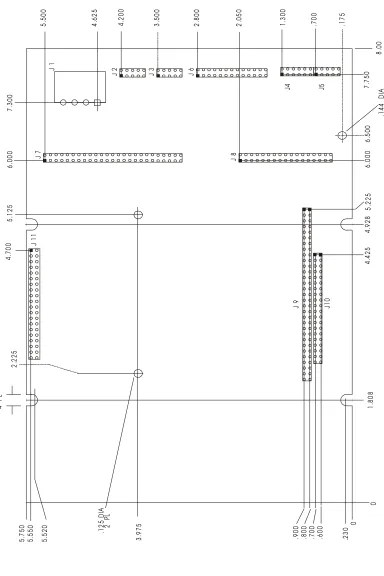
Figure 1-1 Mechanical Dimensions... 1-5
Figure 2-1 Connector and Jumper Locations ... 2-2
Figure 2-2 Byte-Wide Socket Jumpering ... 2-9
Figure 4-1 Little Board/286 Block Diagram ... 4-2
TABLES
Table 2-1 Summary of Connector Usage... 2-1
Table 2-2 Configuration Jumper Summary... 2-3
Table 2-3 "Soft" Configuration Options ... 2-4
Table 2-4 Power Connector (J1) ... 2-5
Table 2-5 Onboard DRAM Memory Size Jumpering... 2-7
Table 2-6 Byte-Wide Device Compatibility ... 2-8
Table 2-7 U32 and U33 Device Jumpering... 2-9
Table 2-8 Video Mode Jumper (W22) ... 2-10
Table 2-9 Utility Connector (J4) ... 2-12
Table 2-10 Keyboard Connector (J5)... 2-14
Table 2-11 Parallel Printer Connector (J6) ... 2-15
Table 2-12 Parallel Printer Port Configuration ... 2-15
Table 2-13 Serial Port Connectors (J2,J3) ... 2-17
Table 2-14 Supported Floppy Formats ... 2-17
Table 2-15 Dual-Speed Drive Option ... 2-18
Table 2-16 Floppy Disk Interface Connector (J8) ... 2-19
Table 2-17 SCSI Interface Connector (J7)... 2-20
Table 2-18A AT Expansion Bus Connector, A1-A32 (J9) ... 2-27
Table 2-18B AT Expansion Bus Connector, B1-B32 (J9) ... 2-28
Table 2-18C AT Expansion Bus Connector, C0-C19 (J10) ... 2-29
Table 2-18D AT Expansion Bus Connector, D0-D19 (J10) ... 2-29
Table 2-19 Interrupt Channel Assignment ... 2-30
Table 2-20 DMA Channel Assignment... 2-30
Table 4-1 Little Board/286 Memory Map... 4-4
Table 4-2 Little Board/286 I/O Map ... 4-5
Table 4-3 Interrupt Channel Assignment ... 4-8
Table 4-4 DMA Channel Assignment... 4-8
Table 4-5 Timer Assignment ... 4-10
CHAPTER 1
INTRODUCTION
1.1 GENERAL DESCRIPTION
The Little Board/286 provides system designers with a high performance, AT-compatible single
board microcomputer system that requires no more space than a half height 5-1/4" disk drive.
This unique single board system is functionally equivalent to a normal AT motherboard and three
or four expansion cards.
The Little Board/286 is ideally suited for embedded microcomputer applications where IBM PC/AT software, hardware, and bus compatibility are required and where low power consumption
(under 9 watts), small size (5.75" x 8" x 1.1"), wide temperature range (0-70o C) and high
reliability are critical. In addition, its ability to use rugged media like EPROM and nonvolatile RAM instead of disk drives makes the Little Board/286 especially well suited for use in harsh environments.
Typical applications for the Little Board/286 include:
n Data acquisition & control n Diskless workstations
n Portable instruments n Point-of-sale terminals
n Protocol conversion n Network servers
n Telecommunications n Distributed processing
n Security systems n SCSI device control
n Intelligent terminals n Vending machines
n Medical instruments n Robot and machine control
The Little Board/286 includes a powerful 12 MHz or 16 MHz 80286 microprocessor, up to 4M bytes of onboard DRAM, and a full complement of AT compatible controllers. Peripheral controllers are included on the board for standard serial, printer, keyboard, speaker, and floppy interfacing. In addition, two industry standard system expansion buses -- a PC/AT Expansion Bus and a Small Computer System Interface (SCSI) -- offer system expansion flexibility.
A PC/AT bus expansion connector is provided for Ampro MinModule expansion boards which attach directly to the Little Board/286. When installed, an onboard MinModule fits entirely within the Little Board/286's outline dimensions.
Standard PC and AT bus plug-in cards can be added to the Little Board/286 using ribbon cable from the PC/AT bus expansion connector. The innovative StackPlane expansion option permits a PC bus card to be mounted parallel to the Little Board/286 without additional hardware. Also available is a compact 2-slot passive backplane which accommodates two PC or AT bus cards.
Support for SCSI direct access devices as boot or data devices is included directly in the board's
ROM-BIOS. This SCSI/BIOS feature allows a wide variety of hard disks, floppy drives, bubble
Sockets on the Little Board/286 allow onboard EPROM (up to 256K bytes) or battery-backed
RAM (up to 64K bytes) to function as a bootable DOS compatible Solid State Disk (SSD) drive.
SSD operation offers several key advantages, including improved speed, reliability, and
ruggedness, as well as reduced power consumption. Ampro's optional SSD support software
converts DOS based applications into EPROM format automatically, without the need for special
programming techniques. In addition, Ampro's SSD Expansion Board, which matche the 5.75" x
8" form factor of the Little Board/286, can be used to add sixteen additional byte-wide device sockets for larger SSD's.
A key advantage of the AT-compatibility of the Little Board/286 is that it runs the thousands of software applications and utility packages developed for IBM's PC and PC/AT. Language compilers, debugging aids, and software support packages for graphics, windowing, multi-tasking, user interfaces, etc., are readily available. In addition, there is a large and growing selection of DOS programs targeted at industrial and commercial applications such as communications, data acquisition and control, terminal emulation, protocol conversion, etc.
The Little Board/286 is a member of Ampro's growing family of IBM compatible single board
1.2 LITTLE BOARD/286 FEATURES
A Complete AT Compatible System on One Board
n All the functions of a motherboard and 4 expansion cards in the
space of a half-height 5-1/4" disk drive!
n Runs standard IBM PC and PC/AT software, including:
-- Disk Operating Systems
-- Languages (C, Pascal, Fortran, Basic,...)
-- Industrial and commercial applications software
n Powerful 12 MHz or 16 MHz 80286 CPU
n Standard AT DMA, timers, and interrupt controllers
n Complete onboard system memory: 512K, 1M, 2M, or 4M bytes
onboard DRAM, and up to 320K bytes EPROM
n Complete set of AT-compatible peripheral ports and controllers:
-- Mini/Micro floppy controller
-- 2 RS232C serial ports, parallel printer port, keyboard port, and
speaker port
-- Optional multi-mode video controller modules
-- Battery-backed real time clock
n Onboard expansion module option:
-- Three choices of onboard display controllers
(EGA/CGA/MDA/Hercules CRT, CGA/MDA/Hercules CRT, CGA compatible LCD)
-- Future onboard modules available (contact factory)
n Industrialized ROM-BIOS, with support for a wide variety of
SCSI devices (hard disk, tape, bubble memory,...) as well as on-and off-board bootable Solid State Disk
Ideal for Embedded Applications
n Low power (mostly CMOS):
-- Uses less than 9 watts of power!
-- Single supply operation (+5V only)
n Wide operating temperature range (0-70o C)
n Reliable:
-- Low component count (30 active components, plus RAM)
-- No backplanes or edgecard connectors required
n Onboard bootable Solid State Disk drive (EPROM/NOVRAM)
option allows diskless DOS operation
n Same form factor and mounting dimensions as a 5-1/4" disk drive
Two Industry Standard Expansion Buses
n AT bus (header) for connection of standard IBM PC and
PC/AT expansion cards
n SCSI bus for addition of Disk/Tape/Optical/Bubble drives,
1.3 LITTLE BOARD/286 SPECIFICATIONS
CPU
n 80286 microprocessor
n CPU clock rate: 12 or 16 MHz
n Half speed option for CPU and/or expansion bus
Onboard Memory
n 512K, 1M, 2M, or 4M bytes DRAM with parity
n Award ROM-BIOS with Ampro extensions
n Two spare 28-pin byte-wide sockets, located at D0000h and
D8000h, usable with:
-- 27256 32K byte EPROM's
-- Intel 27011 128K byte page-addressed EPROM's
-- 62256 32k byte static RAM's
-- Dallas DS1230 32K byte nonvolatile RAM's
-- Dallas DS1217 series NOVRAM cartridges
n 1K bit serial EEPROM, with 512 bits for OEM use
AT-Compatible Controllers
n 2 fully compatible RS232C serial ports
n Parallel printer port with bidirectional data lines
n Standard AT keyboard port
n Speaker port with 0.1 watt output drive
n Standard battery-backed real time clock with 10 year internal lithium battery
n AT-compatible mini (5-1/4") and micro (3-1/2") floppy controller:
-- 2 drive selects, 1-2 sided, 250/500K bps data rates
-- BIOS supports all standard formats (360K/720K/1.2M/1.44M)
-- Reliable all-digital phase-locked loop & write precompensation
-- Disk change sense line support
n Provision for 80287 math coprocessor option
SCSI Interface
n Full ANSI X3.131 (SCSI) compatible
n Uses high performance Adaptec AIC6250 SCSI controller
n Usable as general purpose programmed I/O lines (48 mA sink)
n Over 1.5 megabyte/sec data throughput
Physical
n 8.0 x 5.75 x 1.1 inches (5-1/4 disk drive form factor)
n Mounting slots match 5-1/4" disk drive bottom holes
n Provision for one onboard Ampro MiniModule
n Same DC connector as 5-1/4" disk drives
n Power requirement (with 512K bytes RAM):
-- 80C286 CPU: +5V +/- 5% at 1.6 A (typ.)
-- 80L286 CPU: +5V +/- 5% at 1.8 A (typ.)
n 8-layer PCB, with 2 ground layers for low noise
n Uses latest surface mount technology
n Operating environment:
-- 0-70o C (assuming adequate airflow)
-- 5-95% relative humidity (non-condensing)
0 0 .2 3 0 5. 5 2 0 5. 7 5 0 1. 8 0 8 4. 9 2 8 8. 0 0
J 2 J 3 J 6
J4 J5
J 9 J10
J 8 J 7 J 1 F ig u re 1 -1
. M
e c h a n ic a l D im e ns io ns J 1 1 5. 5 5 0 3. 9 7 5 .1 2 5 D IA 2 P L
.900 .800 .700 .600
5. 22 5 4. 4 2 5 6. 0 0 0 6 .5 00 7. 7 5 0 .1 7 5 .7 0 0 1. 3 0 0 2. 0 5 0 2. 8 0 0 3. 5 0 0 4. 2 0 0 5. 5 0 0 4. 6 2 5 7 .300 6. 0 0 0 5. 1 2 5 4. 7 0 0 2. 2 2 5 .1 44 D IA .1 44 T Y P
4 P
[image:12.612.118.502.73.649.2]CHAPTER 2
HARDWARE CONFIGURATION
2.1 INTRODUCTION
This chapter describes what is required to integrate the Little Board/286 with a wide variety of external devices, including keyboards, printers, modems, floppy and hard disk drives, and monitors. Information is provided regarding the board's connector signals and pinouts, external device requirements, interconnection cable wiring, and board configuration.
Also covered in this chapter are the configuration and initialization requirements of standard and optional onboard devices. These include both the standard items such as the DRAM memory, battery-backed real time clock, and speed control functions, and also several optional additions such as the 80287 math coprocessor, EPROM and NOVRAM "Solid State Disk drives", and a variety of onboard expansion modules including the Ampro MiniModule video controllers.
It is important to note, however, that many of the board's functions are software rather than hardware controlled. Therefore, many of the features and functions described in this manual assume the presence of the board's standard ROM-BIOS for their operation. Refer to Chapter 3 for typical software configuration information, and to Chapter 4 for technical details regarding the board's hardware and software functions.
2 . 1 . 1 Interface Connectors
[image:13.612.214.398.459.592.2]Figure 2-1 shows the location of the board's interface connectors (J1-J11) and configuration jumper locations. Table 2-1 summarizes the use of each of the board's connectors. Connector pinouts and signal definitions are provided in the sections of this chapter that cover each connector interface. Typical interface cable construction data is also included in the description of each connector interface.
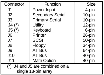
Table 2-1. Summary of Connector Usage
Connector Function Size J1 Power Input 4-pin J2 Secondary Serial 10-pin J3 Primary Serial 10-pin J4 (*) Utility 12-pin J5 (*) Keyboard 6-pin J6 Printer 26-pin J7 SCSI 50-pin J8 Floppy 34-pin J9 AT Bus 64-pin J10 AT Bus 40-pin J11 Math Option 40-pin (*) J4 and J5 are combined on a
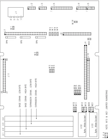
U 1 U 2U 3U 4 U 3 2 U 3 3 J 1 1 J 7 J 8 Fi g u re 2-1. C o n n e c to rs a n d J u m p er s J 1
J 2 J 3 J 6 J 4 J 5
By te W id e S o c ke t By te W id e S o c ke t W1 0 W1 1 W1 4 W1 5 W1 6 W1 7 1 1 1
4 3 2
1 20 21 40 W 1 W 1 9 W2 2
W 3 W 4 W 5 W 6 W 7 W 8 W 9
W 2 B A S E D R A M , LO W B Y TE B A S E D R A M , H IG H B Y TE E X PA N SI O N D R A M , L O W B Y TE E X PA N SI O N D R A M , H IG H B Y TE W1 2 W1 3 W2 0 W2 1 J 1 0 J 9 1 RP 4 RP 5 RP 6 1 3 5 2 4 6 N O TE
: W
[image:14.612.109.467.153.611.2]The board's I/O connectors consist of dual-row male header connectors, of varying lengths. Each of these headers can be mated with either flat ribbon (IDC) or discretely-wired connectors. J2, J3, J4, J5, and J6 have been placed together at one end of the board so that a single header plug can mate with one or more of these connectors as a group.
In some applications it is preferable to plug a specialized PC board assembly onto several or all of the I/O connectors (J2-J8). This allows you to eliminate cables, meet packaging requirements, add EMI filtering, or in other ways customize the installation of the Little Board/286 in your application. In addition, two dual-row male headers provide the PC and AT expansion bus for onboard MiniModule expansion.
2.1.2 Jumper Configuration Options
For normal AT compatible operation, no special jumpering of the Little Board/286 is required. As shipped from the factory, the board can be connected to appropriate peripherals and operated immediately. Typically, the only jumpers you will need to be concerned with are those used for setting the amount of onboard DRAM memory and for specifying whether the powerup video mode is monochrome or color. Table 2-2 summarizes the board's jumper options; they are each discussed in detail in this chapter.
Each of the board's jumper options is referred to by a "W" number (i.e. "W1"). Jumpers occur in 2-pin groups, 3-pin groups, and 6-pin groups. The pin numbering convention for all two- and three-pin jumper groups is as follows: assuming that the card edge connectors are at the bottom
and the I/O connectors are at the right-hand side (Figure 2-1), "pin 1" is topmost on a vertically
oriented line of jumper pins, or leftmost on horizontally oriented pins.
In the case of 2-pin jumper groups, the pair of jumper pins is either shorted or unshorted by installing or removing a shorting block. For three-pin jumper options, there are three choices: shorting pin 1 to pin 2; shorting pin 2 to pin 3; or shorting neither.
[image:15.612.203.413.474.563.2]Two jumper groups (W13 and W21) each have 6 pins. The pin numbering and settings for these four 6-pin jumper groups are discussed later in this chapter.
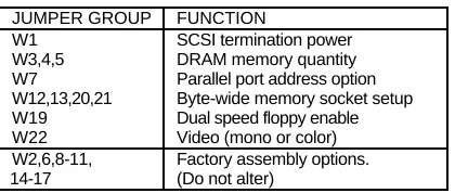
Table 2-2. Configuration Jumper Summary
JUMPER GROUP FUNCTION
W1 SCSI termination power W3,4,5 DRAM memory quantity W7 Parallel port address option W12,13,20,21 Byte-wide memory socket setup W19 Dual speed floppy enable W22 Video (mono or color) W2,6,8-11, Factory assembly options. 14-17 (Do not alter)
2.1.3 "Soft Configuration" Options
In addition to the various configuration jumper options, there are a number of system configuration parameters, which are initialized by the ROM-BIOS based on the contents of two different nonvolatile memory devices on the board -- an AT compatible nonvolatile static RAM within the real time clock device, and a unique 1024 bit configuration EEPROM).
The combination of these two devices will be referred to as the board's nonvolatile Configuration
(CTRL-ALT-ESC) or through the SETUP program on the Little Board/286 Utilities diskette.
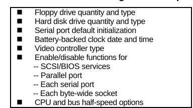
[image:16.612.205.397.149.257.2]Table 2-3 lists the main functions that are controlled by the contents of the nonvolatile Configuration Memory.
Table 2-3. "Soft" Configuration Options
n Floppy drive quantity and type
n Hard disk drive quantity and type
n Serial port default initialization
n Battery-backed clock date and time
n Video controller type
n Enable/disable functions for -- SCSI/BIOS services -- Parallel port -- Each serial port -- Each byte-wide socket
n CPU and bus half-speed options
As shipped from the factory, the Little Board/386 can be booted from a bootable DOS diskette in a 5-1/4" 360K byte floppy drive. You can use the "hot-key" entry into SETUP to set system parameters prior to boot. Using SETUP, you can also load system setup parameters from a disk file, which is useful when configuring systems in a production environment. Refer to Chapter 3 and Appendix A for detailed information on the functions and use of SETUP which is used to initialize these parameters in the board's nonvolatile Configuration Memory devices.
2.2 DC POWER INPUT
The power connector, J1, has a pinout which is identical with that of power connectors on nearly
all 5-1/4 inch disk drives, except that only the +5 volt and ground connections are used. Note
that pin 1 on J1 is reversed from that of the header connectors on the Little Board/286. Refer to Table 2-4 for power connections and mating connector information, and Figure 2-2 for typical connector wiring.
Caution
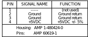
Table 2-4. Power Connector (J1)
PIN SIGNAL NAME FUNCTION 1 --- (not used) 2 Ground Ground return 3 Ground Ground return 4 +5VDC +5VDC +/- 5%
Housing: AMP 1-480424-0 Pins: AMP 60619-1
4 3 2 1
J1
Little Board
+5V GND GNDPower ConnectorLittle Board
GND GND +5V 3
4 2 1
Cable Connector Wiring
No Connect N/C
Figure 2-2. Power Connector Wiring
The precise power requirements of the Little Board/286 depend on a number of factors, including what functions are present on the board (e.g., expansion DRAM, byte-wide memory devices, 80287/80C87 math coprocessor), whether the SCSI bus is terminated, and what peripherals are connected to the board's I/O ports. For example, AT keyboards draw their power from the keyboard connector on the board, and therefore add to the total power drawn by the board from its power supply. Similarly, boards installed in the onboard expansion module position or connected to the AT Expansion Bus may draw their power through the Little Board/286.
Assuming a CMOS 80C286 processor is in use, a fully populated Little Board/286 having 1
megabyte of SIMM RAM installed (without the math coprocessor or MiniModules installed)
requires approximately 8 watts of power (1600 mA). Note that the SCSI bus terminators consume approximately .8 watts of power by themselves, so it is important not to have them
plugged into the board if SCSI is not needed. Operating the CPU with the half-speed option
[image:17.612.105.478.96.443.2]2.3 ONBOARD DEVICE OPTIONS AND CONFIGURATION
This section includes the configuration and installation of onboard devices and options. These
include DRAM and byte-wide memory devices, nonvolatile RAM cartridges, math coprocessor, and a variety of onboard expansion MiniModules including the Ampro MiniModule video controllers.
2.3.1 CPU and Bus Half-Speed Options
The speed of the CPU or of the AT Expansion Bus can be switched to one-half of the normal clock speed under software control. This is set using the Ampro SETUP or SETSPEED utilities, as described in Chapter 3.
When the CPU speed is set to "half-speed," then the AT Expansion Bus speed will also run at half-speed, since it cannot exceed that of the CPU. In addition, it should be noted that the DMA
controller runs at one-half of the CPU rate, so its speed is linked to the setting of the CPU
half-speed option, not the bus half-half-speed option.
Reducing the CPU speed can be useful in lowering system power consumption for battery powered applications, or in increasing the system operating temperature range by reducing the amount of heat generated by key system components such as the DRAM memory.
Operation of the AT Expansion Bus at half speed may be required to allow the use of plug-in cards which were designed to be used in older PC compatible systems with lower system clock rate, or to permit the use of longer bus expansion cables.
The initial state of the CPU and bus half-speed options is determined by parameters stored in the nonvolatile Configuration Memory, which you can set using the Ampro SETUP utility. During system operation, the values of CPU and bus half-speed options can be altered dynamically as desired, using the Ampro SETSPEED utility. Refer to the information on the use of the SETUP and SETSPEED utilities in Chapter 3 and Appendix A for details.
2.3.2 DRAM Memory
The board has positions for up to four s ingle i n-line m emory m odules (SIMM's), which are
organized as either 256K x 9 bits or 1M x 9 bits depending on the version of the Little Board that you are using. At least two SIMM's are required for operation, and the board must be jumpered to indicate whether two or four are being used. Note that when only two SIMM modules are used, they must be inserted in positions U1 and U2, with U3 and U4 left empty.
An additional jumper option, available for systems with 1 megabyte or more of DRAM memory installed, allows the memory above the normal 640K byte system memory area to be used as "extended memory" if desired. When the extended memory option is enabled, it begins at address 100000h.
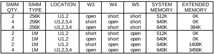
Three jumpers (W3, W4, W5) must be set as shown in Table 2-5, to indicate the number (2 or 4)
and type (256K or 1M) of onboard SIMM DRAM memory that is installed. Note that all four
Table 2-5. Onboard DRAM Memory Size Jumpering
SIMM QTY.
SIMM TYPE
LOCATION W3 W4 W5 SYSTEM MEMORY
EXTENDED MEMORY 2 256K U1,2 open short short 512K 0K 4 256K U1,2,3,4 short open short 640K 0K 4 256K U1,2,3,4 open short short 640K 384K 2 1M U1,2 short short open 512K 0K 2 1M U1,2 open short open 640K 0K 2 1M U1,2 short open open 640K 1408K 4 1M U1,2,3,4 open open open 640K 3456K
On a 12MHz system, use 120 nS (or faster) SIMMs. On a 16MHz system, use 100 nS (or faster) SIMMs.
An additional set of six jumpers (W10, W11, W14-W17) is factory set according to both the board's CPU clock rate and the DRAM memory's access time requirement. These are factory settings, and should not be altered.
2.3.3 Math Coprocessor
Signals for interfacing with a standard 80287/80C287 floating point coprocessor are provided at J11, which is identical in pinout with the normal 40-pin DIP socket, but on .1" row-to-row
spacing. An 80287/80C287 Carrier assembly, available from Ampro, allows you to install a
80287 math coprocessor at this location.
The required speed of the 80287/80C287 math coprocessor is 2/3 the clock rate of the CPU. Therefore the 12 MHz Little Board/286 requires an 8 MHz device (80287-8), while the 16 MHz board requires a 10 MHz device (80287-10).
N o t e
Be sure to install the 80287 on the 80287 Carrier with the IC's pin 1 correctly positioned in pin 1 of the IC socket; be sure to install the 80287 Carrier on the Little Board/286 so that it overlaps the board (pin 1 of J11 mates with 80287 Carrier socket receptacle 1).
When installed on J11, the 80287 math coprocessor is compatible with that of a standard AT computer in all operational details.
N o t e
2.3.4 Byte-Wide Memory Sockets
The Little Board/286 has two onboard byte-wide memory device sockets that can accommodate a variety of EPROM and nonvolatile RAM (NOVRAM) devices, used for simple program storage or as "Solid State Disk" (SSD) drives.
Some of the byte-wide devices which can be used in these sockets are shown in Table 2-6. The NOVRAM cartridges described in the table connect with a short ribbon cable (Dallas P/N DS9000) to a byte-wide socket: U32 or U33. Devices used in these sockets must be 300 nS (or faster), on both 12 MHz and 16 MHz boards.
Table 2-6. Byte-Wide Device Compatibility
DEVICE TYPE SIZE PART NUMBER Normal EPROM (*) 8K bytes Intel 2764 Normal EPROM (*) 16K bytes Intel 27128 Normal EPROM 32K bytes Intel 27256 Page-addr EPROM 128K bytes Intel 27011 Static RAM (*) 8K bytes Hitachi 6264 Static RAM 32K bytes Hitachi 62256 28-pin NOVRAM 32K bytes Dallas DS1230 NOVRAM Cartridges 32K-512K bytes Dallas DS1217 (*) Note: 8K byte EPROM's and static RAM's will appear four times,
and 16K byte EPROM's two times, within the 32K address window of the socket.
Direct Program Access
The memory devices installed in U32 and U33 can be accessed directly by your application software, provided the program knows about them. Note that the byte-wide sockets must be enabled prior to use using the SETUP configuration program (see Chapter 3) or under control of your application program (see Chapter 4).
The byte-wide memory sockets reside at the following memory addresses:
n U32 is at D0000h
n U33 is at D8000h
Through a technique known as a "ROM-BIOS extension", it is possible to have the system run its entire application from byte-wide socket memory devices, instead of from disk drives. This is discussed in Ampro application note AAN-8702. Be sure the sockets are enabled, as mentioned above, if they are to be used with ROM-BIOS extensions.
Solid State Disk (SSD) Drives
Using the Ampro SSD software, the byte-wide sockets can serve as individual SSD drives, or they can be combined into one larger drive. SSD drives can be used along with normal (floppy and hard disk) drives. Ampro's SSD Expansion Board provides additional SSD sockets.
Byte-Wide Socket Configuration
If the byte-wide memory sockets are used, they must be configured by means of jumpers for the device type in use. W12 and W13 are associated with U32, while W20 and W21 are associated with U33.
[image:21.612.144.450.277.435.2] [image:21.612.174.409.470.629.2]The supported memory devices and corresponding jumper settings are shown in Table 2-7. Note that W13 and W21 each consist of six jumper pins, numbered "1" through "6", as shown in Figure 2-3.
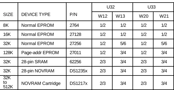
Table 2-7. U32 and U33 Device Jumpering
U32 U33 SIZE DEVICE TYPE P/N W12 W13 W20 W21
8K Normal EPROM 2764 1/2 1/2 1/2 1/2 16K Normal EPROM 27128 1/2 1/2 1/2 1/2 32K Normal EPROM 27256 1/2 5/6 1/2 5/6 128K Page-addr EPROM 27011 1/2 3/4 1/2 3/4 32K 28-pin SRAM 62256 2/3 3/4 2/3 3/4 32K 28-pin NOVRAM DS1235x 2/3 3/4 2/3 3/4 32K
to
512K NOVRAM Cartridge DS1217x 2/3 3/4 2/3 3/4 The required access time for devices plugged into U32 and U33 is 300 nS or faster.
1 2 3 1
W12
2 W13
1 3 5
1 2 3 1
W20 2 W21
1 3 5
Figure 2-3. Byte-Wide Socket Jumpering
In addition to having its device configuration jumpers set, each socket must be enabled or
disabled via a parameter within the board's nonvolatile Configuration Memory. The Ampro SETUP utility offers a convenient means to do this. SETUP resides in the ROM-BIOS and can be accessed either with a "hot-key" entry (CTRL-ALT-ESC) or through the SETUP program provided on the Little Board/286 Utilities diskette.
n U32
n U33
4
4
4
As mentioned previously, the required access time for devices plugged into U32 and U33 is 300 nS (or faster), on both 12 MHz and 16 MHz boards.
N o t e
When a byte-wide memory device is enabled, its memory address space is unavailable for use by other devices on the AT bus. A byte-wide socket must be marked as "disabled" by means of the Ampro SETUP utility before its memory space can be used for other purposes.
2.3.5 Battery-Backed Clock
The Little Board/286 provides, as a standard feature, an AT compatible battery-backed real time clock (with CMOS RAM). Included within the clock module is a lithium battery, so no external backup battery is required. At ten-year intervals, the entire device should be replaced. Oversized solder pads have been provided to facilitate this maintenance operation.
The real time clock date and time values and various parameters within the nonvolatile Configuration Memory are initialized at the factory for a standard configuration. The date and time are also set at the factory, but may not be set for your time zone. Use the Ampro SETUP utility to change these values as needed (see Chapter 3).
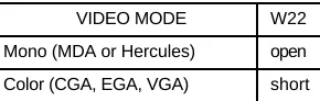
2.3.6 Video Display Mode Jumpering
Regardless of what type of video display controller is used -- whether by means of an onboard video expansion module or by means of a controller connected externally on the AT Expansion Bus -- a jumper (W22) on the Little Board/286 must be properly configured to indicate to the
ROM-BIOS whether the board's powerup (or reset) video state should be color or monochrome.
[image:22.612.234.379.480.526.2]W22 is jumpered as indicated in Table 2-8.
Table 2-8. Video Mode Jumper (W22)
N o t e
When an EGA or VGA controller's switches or jumpers are configured for a monochrome mode, W22 should be set for "color" rather than "mono".
The function of W22 is replicated on the Utility Connector (J5) pins 9 and 10. This was done to facilitate the use of an external mono/color configuration switch, if needed. Pins 9 and 10 of J5 are not normally populated with connector pins, so you must add pins in that location if you wish to take advantage of the option.
In addition to setting W22, the desired bootup video mode must also be specified in the board's nonvolatile Configuration Memory. The Ampro SETUP utility offers a convenient means to do this. SETUP resides in the ROM-BIOS and can be accessed either with a "hot-key" entry (CTRL-ALT-ESC) or through the SETUP program provided on the setting of W22 and the parameters in the Configuration Memory do not match, an error message will be displayed during the system boot process.
N o t e
When an EGA or VGA controller is configured to bootup in a monochrome or CGA mode, the video controller type parameter specified using the SETUP utility should still be set for "EGA" or "VGA".
Also, don't forget to set any appropriate switches or jumpers on the video display controller for
2.4 PERIPHERAL CONNECTIONS AND CONFIGURATION
This section covers the interface requirements of the board's external device interface connectors. Information is provided on interface and device characteristics, connector pinouts, signal definitions, jumper configuration, and nonvolatile Configuration Memory setup.
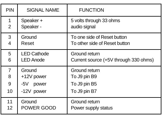
2.4.1 Utility Connector
[image:24.612.174.438.265.452.2]A single 12 pin connector (J4) provides five functions: Speaker, Reset, Power Indicator LED, auxiliary power to the AT Expansion Bus connector (J9), and a Power Good status signal. The pinout and signal definitions of the Utility Connector are shown in Table 2-9. Note that the power connections indicated are not required for operation of the Little Board/286, and are only used to provide power for cards connected to the board's AT Expansion Bus connector.
Table 2-9. Utility Connector (J4)
PIN SIGNAL NAME FUNCTION
1 Speaker + 5 volts through 33 ohms 2 Speaker - audio signal
3 Ground To one side of Reset button 4 Reset To other side of Reset button
5 LED Cathode Ground return
6 LED Anode Current source (+5V through 330 ohms)
7 Ground Ground return 8 +12V power To J9 pin B9 9 -5V power To J9 pin B5 10 -12V power To J9 pin B7
11 Ground Ground return 12 POWER GOOD Power supply status
Speaker
The board provides an AT compatible speaker output on two pins (1,2) of the Utility Connector. The speaker signal is buffered by a transistor amplifier to provide approximately .1 watt of audio power to an external speaker. Typically, a small general purpose 2 or 3 inch diameter permanent magnet speaker with an 8 ohm voice coil is used.
Speaker tones can be generated either by directly bit-banging the speaker control port or by setting
Timer 2 to a desired frequency tone and enabling the tone with an enable port. Refer to an AT technical reference manual for custom programming information.
Pushbutton Reset
Power Indicator LED
Two pins (5,6) of the Utility Connector provide connections for an external power indicator LED device. 15 mA of sourced current is available (+5V through 330 ohms). Pin 5 goes to the LED's cathode, and 6 to its anode.
AT Bus Power Options
Four pins (7,8,9,10) of the Utility Connector allow the connection of an external source of +12VDC, -5VDC, and -12VDC power to the board's AT bus (J9) for use by plug-in expansion cards. The Little Board/286 does not require these voltages.
Power Good Signal
Two pins (11,12) of the Utility Connector provide connections for a power good signal from
power supplies which offer this feature. The purpose of this signal is hold the system in a reset state when power is not within the proper range. This signal connects to the board's reset circuitry, and is functionally equivalent to the Pushbutton Reset (pin 4). This input has a TTL level, Schmitt trigger conditioned input buffer, and requires an active low input of 1 second minimum duration for the system to reset reliably.
2.4.2 Keyboard
An AT compatible keyboard can be connected to the board's keyboard port via the first five pins (1-5) of connector J5. Normally, AT keyboards include a cable which terminates in a male 5-pin DIN plug for connection to an AT. Table 2-10 gives the board's keyboard connector pinout and signal definitions, and includes corresponding pin numbers of a normal AT DIN keyboard connector.
Pin 6 of J5 can be connected to a keyboard inhibit switch. When this pin is grounded, keyboard
inputs will be ignored. This can be used with key operated switches for system security.
Four additional locations (7,8,9,10) of J5 are not ordinarily populated with connector pins. Of these, pins 7 and 8 are not connected, while pins 9 and 10 duplicate the function provided by W22, the video mode jumper (discussed earlier). If required, you can include the video mode jumper function in a cable assembly for external access.
N o t e
Table 2-10. Keyboard Connector (J5)
J5 PIN SIGNAL NAME DIN PIN 1 Keyboard Clock 1 2 Keyboard Data 2 3 (no connection) 3
4 Ground 4
5 Keyboard power 5 6 Keyboard inhibit 7 (*) No connect
8 (*) No connect 9 (*) Same as W22-1 10 (*) Same as W22-2 (*) = No connector pins.
2.4.3 Parallel Printer Port
The board's serial/parallel controller option (U22) must be installed for this function to be available. The parallel printer connector (J6) has a pinout that allows the use of flat ribbon cable to a standard DB25S PC or AT rear panel printer connector. Table 2-11 gives the printer connector's pinout and signal definitions.
The table also indicates the pin number on the AT compatible DB25 printer connector which corresponds to each of the pins of the board's header connector. Note that the pin numbering convention for the board's header connector differs from that of DB25 connectors, even though direct connection with flat ribbon cable is possible. To clarify this, each signal's corresponding DB25 connector pin number has been included in the table.
N o t e
Be sure not to exceed 10 feet of total cable length between the board's connector and the printer. Beyond this distance, the signal cannot be expected to be reliable due to the limitations of the port's signal drivers.
Table 2-11. Parallel Printer Connector (J6)
J6 PIN
SIGNAL NAME FUNCTION IN/OUT DB25 PIN 1 -STROBE Output data strobe out 1 3 Data 0 LSB of printer data i/o 2
5 Data 1 : i/o 3
7 Data 2 : i/o 4
9 Data 3 : i/o 5
11 Data 4 : i/o 6
13 Data 5 : i/o 7
15 Data 6 : i/o 8
17 Data 7 MSB of printer data i/o 9 19 - ACK Character accepted in 10 21 BUSY Cannot receive data in 11 23 PAPER OUT Out of paper in 12 25 SEL OUT Printer selected in 13 2 -AUTOFD Autofeed out 14 4 -ERROR Printer error in 15 6 -INIT Initialize printer out 16 8 SEL IN Selects printer out 17 26 -POE Port output enable in --10,12
14,16 18,20
22,24 GND Signal Ground --- 18-25
Printer Port Configuration
The jumper at W7 is provided to allow this port to be configured as either a primary or secondary
AT compatible printer port. The jumper must be set as indicated in Table 2-12. When shipped,
the board is configured for the primary option. In addition, the board's nonvolatile Configuration
Memory contains a parameter which can be used to disable the port entirely. Use the Ampro
SETUP utility to disable the parallel port, if desired.
Table 2-12. Parallel Printer Port Configuration
SELECTION I/O ADDR. INTERRUPT W7 “Primary” 378-37Fh IRQ7 open “Secondary” 278-27Fh IRQ5 short
As seen in Table 2-12, jumper option W7 allows a choice of two I/O port addresses for the printer port (378-37Fh or 278-27Fh).
Normally, DOS assigns the name "LPT1" to the primary device, and "LPT2" to the secondary
printer device (if present). However, a scan is made for both choices (primary and secondary) and
if only a secondary printer is detected, it will be assigned as the "LPT1". Therefore, to avoid
confusion, the board's printer port should always be configured for the primary assignment shown
[image:27.612.201.411.437.485.2]N o t e
There is no means to alter the printer port's interrupt, so although its I/O port address can be set to the standard LPT1 or LPT2 values, its interrupt remains at IRQ7. DOS does not use the interrupt, while some printer port control software does (such as print spoolers).
Bidirectional Parallel Port Usage
The parallel printer port can be used as a normal AT printer port, or it can be used for general purpose programmable I/O. By using the port's input and output handshake signals on along with its 8-bit bidirectional data lines, many types of interfaces for specialized devices can be created, including writing data to LCD display panels, scanning keyboards, etc.
When configured as a bidirectional data bus, the parallel port cannot be used to support a standard printer.
Refer to Chapter 3 for typical system software configuration information, and to Chapter 4 for hardware details regarding nonstandard uses of this interface.
2.4.4 Serial Ports
The board's serial/parallel controller option (U22, U15, U16, U8, and associated circuitry) must be installed for the serial port function to be available. Two AT (and PC) compatible serial ports appear at header connectors J2 and J3. Each provides three RS232C output signals and five RS232C input signals, to facilitate connecting a broad range of serial devices to the Little Board/286 on either port (see Table 2-13).
Both ports support software selectable standard baud rates up to 19.2K bits/second (limited by the RS232C drivers), 5-8 data bits, and 1, 1.5, or 2 stop bits. The serial ports appear at the standard port addresses of 3F8-3FFh (primary port) and 2F8-2FFh (secondary port), using interrupts IRQ4 and IRQ3, respectively.
These two serial ports can be used for connection of printers, modems, terminals, remote hosts, or other serial devices. The main interface consideration is that the device be RS232C compatible. Many devices, such as printers and modems, require handshaking in one or both directions. Consult the documentation of the external serial device for information regarding possible handshake and other interface considerations.
Support in the ROM-BIOS allows a device connected via one of the board's serial ports to be used as the system "console" (keyboard and display), as an alternative to the use of a video controller, monitor, and keyboard. This is further discussed in Chapter 3.
Pin 10 of each serial port connector is an enable signal which is normally left unconnected
When it is brought to a TTL high level, it disables the input signals. It is pulled low on the board by a 1K ohm resistor. This signal is intended for board test purposes only.
J3 is the primary serial port, and is supported by the board's ROM-BIOS as the DOS "COM1"
device. The secondary serial port is J2; it is supported as the "COM2" device. However, it is
possible to disable either or both serial ports using the Ampro SETUP utility. (Note: if you disable the primary port and enable the secondary port, then the secondary port gets installed as COM1 by DOS, unless there is a primary port present somewhere else in the system.)
Table 2-13. Serial Port Connectors (J2,J3)
PIN SIGNAL NAME
FUNCTION IN/OUT DB25 PIN
DB9 PIN 1 DCD Data Carrier Detect in 8 1 2 DSR Data Set Ready in 6 6 3 RXD Receive Data in 3 2 4 RTS Request To Send out 4 7 5 TXD Transmit Data out 2 3 6 CTS Clear To Send in 5 8 7 DTR Data Terminal Ready out 20 4 8 RI Ring Indicator in 22 9 9 GND Signal Ground -- 7 5 10 EN Input Enable in --
--2.4.5 Floppy Disk Interface
[image:29.612.178.433.211.314.2]The board's floppy controller option (U34) must be installed for this interface to be available. The onboard floppy disk controller and ROM-BIOS support one or two floppy disk drives in any of the standard DOS formats shown in Table 2-14.
Table 2-14. Supported Floppy Formats
CAPACITY DRIVE SIZE TRACKS DATA RATE DOS VERSION REQUIRED 360K 5-1/4” 40 250 KHz 2.1+
1.2M 5-1/4” 80 500 KHz 3.0+ 720K 3-1/2” 80 250 KHz 3.2+ 1.44M 3-1/2” 80 500 KHz 3.3+
Floppy Drive Considerations
As indicated in Table 2-14, nearly any type of soft-sectored, single or double-sided, 40 or 80 track, mini or micro floppy disk drive is usable. Naturally, the higher the quality of the drives you use, the better your system's reliability. Here are some general considerations regarding the selection, configuration, and connection of floppy drives to the Little Board/286.
n Drive Interface -- The drives used must be compatible with the board's floppy disk
n Drive Quality -- High quality, DC servo direct drive motor floppy disk drives are recommended.
n Drive Combinations -- Any combination of supported drives can be used.
n Drive Select Jumpering -- Both drives must be jumpered to the second drive select. Use a
floppy cable with a segment of wires "twisted" as is the usual practice in PC and AT compatible systems.
n Drive Termination -- Resistive terminations should be installed only on the drive
connected to the last interface cable connector (farthest from the computer).
n Head Load Jumpering -- When using drives with a Head Load option, jumper the drive
for "head load with motor on" rather than "head load with drive select."
n Drive Mounting -- If the computer board is to be mounted directly on a disk drive, it is
recommended that a thin metal shield be used between the disk drive and the computer board, to reduce the possibility of electromagnetic interactions. A drive and board mounting bracket is available as an option from Ampro.
n Dual Capacity Drives -- The Little Board/286's ROM-BIOS allows dual-capacity use of a
1.2 megabyte "high density" drive: i.e., 360 Kbyte diskettes can be read on a high density drive. However, it is not recommended that you write to 360K diskettes on the high density drive, as incomplete erasure may occur. (This recommendation applies to standard AT's as well.) In addition, there are two types of floppy drives that offer dual-capacity operation:
--Standard AT drives: the data rate shifts between 250K and 500K bits/second, but the
drive's rotationalspeed stays constant.
--Dual speed drives: the data rate shifts between 250K and 300K bits/second, and the
drive's rotational speed changes between 300 and 360 rpm as well.
A jumper (W19) is used to select between the two types of dual capacity drives. Refer to Table 2-15.
Table 2-15. Dual-Speed Drive Option
W19 FUNCTION
short Dual-speed operation enabled open Dual-speed operation disabled
Floppy Interface Configuration
The desired configuration of floppy drives (number and type) must be properly initialized in the board's Configuration Memory. This is generally done using the Ampro SETUP utility. In addition, the dual-speed configuration jumper option (W19) should be set according to whether
Floppy Interface Connector
Table 2-16 shows the pinout and signal definitions of the board's floppy disk interface connector, J8. J8 is identical in pinout with the floppy connector of standard AT and PC floppy controller
boards. Note that, as in a standard PC or AT, both floppy drives are jumpered to the same drive
[image:31.612.201.413.214.388.2]select -- as the "second" drive. The drives are uniquely selected as a result of a swapping of a group of seven wires (conductors 10-16) that must occur in the cable between the two drives. The seven-wire swap goes between the computer board and drive "A"; the wires to drive "B" are unswapped (or swapped a second time).
Table 2-16. Floppy Disk Interface Connector (J8)
PIN SIGNAL NAME FUNCTION IN/OUT
2 -RPM/-RWC Speed/Precomp out 4 --- (Not used) ---6 --- (Not used) ---8 -IDX Index Pulse in 10 -MO1 Motor On 1 out 12 -DS2 Drive Select 2 out 14 -DS2 Drive Select 1 out 16 -MO2 Motor On 2 out 18 -DIRC Direction Select out
20 -STEP Step out
---2.5 SCSI INTERFACE
The board's Small Computer System Interface (SCSI) controller option (U7 and associated components) must be installed for this interface to be available. The SCSI interface uses a 50-pin male header connector (J7) to interface with SCSI compatible peripherals. Table 2-17 shows the pinout and signal definitions of this interface. Refer to your SCSI device documentation, or the ANSI X3.131 SCSI specification (referenced in Chapter 4) for detailed information on the signal functions. Be sure that the maximum total SCSI bus cable length, from the board's connector to the most distant SCSI peripheral, does not exceed 18 feet.
N o t e
[image:32.612.201.412.334.563.2]If the SCSI interface is not needed, you should either disable it by using the SETUP utility or by placing a shorting block on pins 1 and 2 of the SCSI connector (J7). When the shorting block is in place, the system bypasses any attempt to boot from the SCSI device, which can speed up the boot process.
Table 2-17. SCSI Interface Connector (J7)
PIN SIGNAL FUNCTION 2 -DB0 Data Bit 0 (LSB) 4 -DB1 “ “ 1 6 -DB2 “ “ 2 8 -DB3 “ “ 3 10 -DB4 “ “ 4 12 -DB5 “ “ 5 14 -DB6 “ “ 6 16 -DB7 “ “ 7 (MSB) 18 -DBP Data Parity 26
TERMPWR
Termination +5VDC 32 -ATN Attention
34 GROUND Signal Ground 36 -BSY Busy
38 -ACK Transfer Acknowledge 40 -RST Reset
42 -MSG Message 44 -SEL Select 46 -C/D Control/Data 48 -REQ Transfer Request 50 -I/O Data Direction 25 --- Not used 1-49 (odd)
2.5.1 Normal Use of SCSI
The board's SCSI bus interface can serve a variety of purposes, including connection of hard disk controllers, tape controllers, text scanners, and printer and communications servers. Support is provided by the board's ROM-BIOS for booting of DOS from a SCSI device such as a hard disk.
Virtually any device compatible with the SCSI Common Command Set for direct access devices
can be used through the ROM-BIOS support. Some examples of direct access SCSI devices that can be accessed as DOS drives are hard disk drives, magnetic bubble drives, high density floppy drives, and some tape drives.
The Little Board/286 comes with a diskette containing software drivers and utilities for normal DOS operation using hard disks and other SCSI direct access devices. Included are a formatter, a partition editor, and a device driver capable of multiple drive and partition operation. Refer to Chapter 4 for information on software setup and drive preparation.
PC-DOS version 3.x requires that drives larger than 32 megabytes be partitioned into more than one "partition", while DR-DOS and PC-DOS 4.x allow a maximum partition size of 128M bytes. If desired under PC-DOS 3.x, each physical drive can be have a maximum of up to four partitions, 32 megabytes or smaller, allowing the use of drives as large as 128 megabytes. PC-DOS 4.x and DR-DOS limit drive size to 512M bytes (four 128M byte partitions).
There are several other types of SCSI devices besides direct access devices. SCSI's additional
device types include sequential access devices (e.g. tape), printer devices, read-only devices (e.g.
CD-ROM), and processor devices (e.g. CPU's). In general, these other device types require
special application programs, utilities, or driver software for use. For example, Ampro offers an optional tape backup program which can be used for DOS environment hard disk backup.
Hard disk support for operating systems other than DOS may or may not be automatically available through the board's ROM-BIOS resident hard disk driver. This depends on whether the operating system in question uses BIOS calls exclusively for the hard disk function, and whether the operating system has any special ROM-BIOS constraints (such as re-entrancy). Some operating systems -- multitasking ones in particular such as Unix -- interface directly with the hardware (e.g. attempt to directly program an AT compatible hard disk controller) and bypass BIOS. In those situations, the operating system must be modified to add an appropriate SCSI hard disk driver to use the to take advantage of the board's SCSI interface. An alternative is to use the Ampro MiniModule/ATDisk controller board interface, which provides compatibility with standard ATA-equipped hard disk drives. Refer to the Ampro MiniModule/ATDisk Technical Manual for additional information regarding the board's capabilities.
2.5.2 The Ampro SCSI/BIOS
Through the universal bus interface and command protocols offered by SCSI, it has become possible to connect a wide variety of mass storage devices to a computer system with virtually no
changes to system software. To this, Ampro has added a further layer of universality: the
As its name implies, the SCSI/BIOS consists of a set of low level functions which have been incorporated into the ROM-BIOS to provide a hardware independent interface between system software and peripheral devices connected to the SCSI bus. The advantage of the Ampro SCSI/BIOS is that programmers can write software that uses devices connected to the SCSI bus without having to be concerned with the details of operating the board's SCSI bus interface. Also, software can be "ported" to the Little Board/286 from other hardware environments much faster due to the presence of the SCSI/BIOS, and with less difficulty and risk.
The board's SCSI interface, and the Ampro SCSI/BIOS within the board's ROM-BIOS are discussed in greater detail in Chapters 3 and 4. In addition application note AAN-8804, available from Ampro, provides details of the SCSI/BIOS functions available to programmers.
2.5.3 Simple Bidirectional I/O
When the board's SCSI bus is not needed for interfacing to standard SCSI devices, it can be used instead as a general purpose digital input/output port. The SCSI bus then becomes a set of programmable I/O signals, with TTL signal levels and open collector output drivers capable of sinking 48 mA. In this case, sixteen SCSI bus signals can be used; of these, nine are capable of bidirectional use, and seven are input-only.
The available SCSI port output signals can be "bit banged" (i.e. software activated) to generate a wide variety of signal timings and operations. For example, it is even possible to interface with optically isolated AC and DC input and output modules, and to a number of off-the-shelf data acquisition and control interfaces.
Ampro application note AAN-8801 discusses a typical non-SCSI application. Refer also to Chapter 3 for typical system configuration information, and to Chapter 4 for information about the board's SCSI bus interface.
2.5.4 SCSI Interface Configuration
Several items associated with the board's SCSI interface should be configured according to your system needs:
SCSI Bus Termination
Three 8-pin 220/330 ohm SIP resistor networks (RP4, RP5, and RP6) provide bus termination.
The termination networks should be present on two, and only two, SCSI bus devices. An
improperly terminated SCSI bus may interfere with normal system operation due to indeterminate signal levels.
N o t e
Internally, pins 2-7 of the SIP networks have 220 ohm resistors connected to +5 volts (pin 8), and 330 ohm resistors connected to ground (pin 1).
Note that the SCSI Bus termination networks consume significant power (.8 watt). If power consumption is critical, consider having the bus termination external to the board, and externally powered.
External Termination Power Option
The SCSI specification includes the option of using external bus termination. To accommodate
this feature, the Little Board/286 provides a jumper option (W1), which allows the board to supply termination power (+5V) to the SCSI bus TERMPWR signal (pin 26). A Shottky protection diode is included on the board, as recommended by the ANSI specification, to prevent
board damage from current which might otherwise flow from the SCSI bus.
The default jumpering of this option is unshorted; i.e. termination power is not normally supplied by the Little Board/286.
SCSI Controller Interrupt
Jumper W2, when shorted, connects the board's SCSI interface controller interrupt output signal to interrupt IRQ15 on the AT bus. Though not currently used, the IRQ15 interrupt is reserved for future enhancements of the Ampro SCSI/BIOS. It is recommended that you not use it in your system designs, to preserve compatibility with future Ampro BIOS revisions. Therefore, leave jumper W2 in its factory setting (shorted or unshorted).
"Soft Configuration" Options
Every SCSI device must be configured for a specific SCSI bus ID, between 0 and 7. The SCSI Initiator ID of the Little Board/286 is determined by a parameter stored in the board's Configuration Memory. Use the Ampro SETUP utility to set this value. Normally, the board's SCSI "initiator" ID should be set to 7, and the ID's of the disk drives and other SCSI "target" devices should be set to 0, 1, etc.
Another important SCSI-related option, available via a parameter stored in the Configuration Memory, is whether or not the SCSI/BIOS services in the board's ROM-BIOS are desired. Using
the Ampro SETUP utility, you can disable or enable SCSI/BIOS services. If you set the
parameter to disable the SCSI/BIOS services, there will be no support BIOS support for it at all.
This might be desirable for several reasons:
n To speed system booting when normal SCSI interfacing is not required, such as in a
floppy-only system. Otherwise, there is a delay during system booting, while the system waits to see if a SCSI device at ID0 LUN0 becomes ready.
n To disallow SCSI/BIOS control of the SCSI hardware, when the interface is to be used in a
non-standard manner.
n When using an AT hard disk controller (on the bus, or connected by means of the
2.6 AT EXPANSION BUS
An AT compatible expansion bus appears at connectors J9 and J10, except that it is brought out
to a pair of header connectors, rather than edgecard connectors.
The PC-bus subset of the board's AT Expansion Bus connects to the first 62 pins of J9; the two additional pins of J9 (A32, B32) offer additional ground signals, for enhanced system reliability. The 36-pin edgecard connector, normally included in an AT expansion bus, is replaced by a 40-pin header connector, at J10. As with J9, additional ground connections have been provided. In
this case, there are two additional ground pins at each end of the connector. AT Expansion Bus
connector pinouts are given later in this chapter.
Table 2-18 shows the pinout and signal functions of the signals on the board's AT Expansion Bus and MiniModule headers. Further information about these signals is available in numerous publications, including the IBM technical reference manuals for the PC and AT computers, and from the reference documents listed in the beginning of Chapter 4.
Note that the board's AT Expansion Bus and MiniModule connector pins are numbered differently from the other header connectors on the board, so that they correspond to the scheme normally
used on the PC and AT Expansion Bus. Specifically, rather than being designated numerically
(1, 2, 3, etc.) the signals of the AT Expansion Bus are designated alpha-numerically (A1, A2, ...,
B1, B2, ..., etc).
With the exception of the onboard serial, parallel, and floppy controllers, all signal outputs driving the AT Expansion Bus are rated at 24 mA sink current at a logic "low" level of 0.4 Volts. (The serial and parallel controllers provide 16 mA bus drive, and the floppy controller provides 12 mA.)
N o t e
Most PC and AT bus plug-in cards are intended for use on an 8 MHz bus. It is therefore advisable to use one of the Ampro utilities (SETUP or SETSPEED) to enable the board's AT expansion bus "half-speed" option when PC or AT bus plug-in cards are to be used, unless the cards are known to operate properly at the faster bus speed of the Little Board/286.
2.6.1 Onboard MiniModule Header and Bus Expansion
An important feature of the Little Board/286 is its onboard MiniModule headers. Two header connectors, J9 and J10, provide an AT Expansion Bus interface for use with one of Ampro's 3.6" x 3.8" expansion MiniModules. When installed on J9 (PC bus subset of the AT expansion bus), the onboard expansion module fits within the Little Board/286's space envelope. The onboard
expansion module provides a bus pass-through connector, allowing additional external bus
Several options are available for mounting multiple MiniModules on the Little Board/286:
n Stacker/MM -- Allows two MiniModules to be stacked together and mounted as a single
unit.
n StackPlane/MM -- Provides two expansion bus header connectors for mounting
Mini-Modules on a Little Board form-factor board. When used with the Stacker/MM, up to four MiniModules can be attached. The SSD Expansion board also offers two expansion bus header connectors for mounting MiniModules.
n Pass-through connectors -- The MiniModule/ATDisk controller offers a pass-through
connector, which can be used to stack an additional MiniModule without needing a Stacker/MM.
Ampro currently offers several display controller MiniModules which offer a wide variety of standard PC and AT video modes, including VGA, EGA, CGA, MDA, and Hercules display compatibility, on CRT monitors, LCD panels, and electroluminescent (EL) panels. Ampro also offers additional MiniModules, including serial/parallel interfaces, modems, etc. Contact Ampro for information on additional MiniModules.
2.6.2 Using Standard PC and AT Bus Cards
There are several options available from Ampro which allow you to add expansion cards to the Little Board/286 system:
n StackPlane/PC Expansion Adapter -- a board having the identical dimensions and
mounting points as the Little Board/286. This adapter converts a PC bus add-on card to
the Little Board form factor. The StackPlane/PC adapter piggy-backs above or below the Little Board/286 and connects to J9 (PC bus subset of the AT bus) by means of a short ribbon cable. Several StackPlane/PC adapter assemblies can be stacked.
n MiniBackplane/ATBus -- two-slot AT bus passive backplane with 64-pin and 40-pin male
bus headers for cable connection to J9 and J10 on the Little Board/286. Includes options of onboard +12V, -12V, and -5V DC-to-DC converters, which makes possible complete +5V-only system operation.
n Cable-Mount Edgecard Sockets -- 62-pin and 36-pin edgecard connectors can be used to
construct a ribbon cable which can connect the Little Board/286's AT expansion bus (or PC
bus subset) directly to a PC or AT plug-in expansion card using ribbon cable only. The
edgecard sockets are available from
PCD Connectors Winchester, MA (617) 721-1280
RF18-2582-5 (36-conductor edgecard socket) RF31-2582-5 (62-conductor edgecard socket)
2.6.3 Expansion Bus Cable Considerations
Here are several points regarding the use of the board's AT Expansion Bus:
n Cable Length -- Keep the ribbon cable used as short as possible. Expansion bus cables
in excess of six inches can result in reduced system reliability. We recommend:
-- For cable lengths up to 6 inches, use a high quality ribbon cable, such as 3M part number 3365/64 (64 conductor) and 3365/40 (40 conductor).
-- For cable lengths between 6 and 12 inches, use a high quality ribbon cable with ground
plane, such as 3M part number 3353/64 (64 conductor) and 3353/40 (40 conductor).
-- Cable lengths in excess of 12 inches are not recommended.
n Backplane Quality -- Be sure to use a high quality backplane having minimal signal
crosstalk. Use of power and ground planes, and ground guard traces between bus signals is recommended.
n Reset Deglitching -- Some PC and AT bus expansion cards have asynchronous TTL
inputs that are especially vulnerable to cable noise and crosstalk. In particular, the active high RESET line is one to watch out for. If this signal is found to be susceptible, a 200pf to 500pf capacitor connected between the RESET signal and ground can be used to prevent false expansion card resets. This RESET deglitching capacitor is included on the Ampro MiniBackplanes.
n Bus Half-Speed Options -- Typically PC and AT expansion bus cards are designed for 8
MHz maximum expansion bus speed, though new boards and boards of your own design may allow faster system operation. You can use the Ampro SETUP or SETSPEED
utilities to set bus operation to full- or half-speed. When set to half-speed, the "CLK"
signal on expansion bus pin J9-B20 becomes half the system clock (i.e. 8 MHz on a 16 MHz board, and 6 MHz on a 12 MHz board). Use full-speed bus operation with caution!
2.6.4 Expansion Bus Connector Pinouts
Tables 2-18A through 2-18D indicate the pinout and signal functions of the signals on the board's AT Expansion Bus connectors. Further information about these signals is available in numerous publications, including the IBM technical reference manuals for the PC and AT computers, and from the reference documents listed in the beginning of Chapter 4.
The board's AT Expansion Bus header connector (J9 and J10) pins have been numbered differently from the other header connectors on the board, so that they correspond to the scheme normally used on PC and AT bus edgecard connectors. The even numbered pins correspond to the "B" and "D" rows of the AT bus; and the odd numbered pins correspond to the "A" and "C" rows (e.g. J9 pin 1 is labeled "B1"). The first 62 pins of J9 (beginning at A1 and B1) are the ones which correspond to the 62 conductors of the PC bus subset of the AT backplane. The last
two pins are spare grounds. On J10, however, the middle 36 pins (out of 40, total) correspond
to the AT bus 36 conductor edgecard connector, with 2 spare grounds at each end of the board's