Int. J. Electrochem. Sci., 9 (2014) 2944 - 2954
International Journal of
ELECTROCHEMICAL
SCIENCE
www.electrochemsci.org
Concentration Dependent Optical and Structural Properties of
Mo doped ZnTe Thin Films Prepared by e-beam Evaporation
Method
Shailaja Jeetendra1, H. Nagabhushana2, K. Mrudula1, C. S. Naveen1, P.Raghu1, H. M. Mahesh1,*
1
Department of Electronics Science, Bangalore University, Jnanabharathi, Bangalore – 560056, India
2
Department of PG Studies and Research in Physics, Tumkur University, Tumkur – 572 103, India
*
E-mail: [email protected]
Received: 24 January 2014 / Accepted: 2 March 2014 / Published: 23 March 2014
ZnTe doped with different concentrations of Molybdenum (Mo) thin films were prepared by e- beam evaporation method and the effect of doping on Optical and Structural properties of the thin films were studied. XRD results confirmed the doping of Mo through its signature peaks at 27.6 for MoTe2 (011)
and 38.40 for Mo (220) along with the ZnTe (111) peak at 25.3. AFM images indicated the crystalline nature of ZnTe:Mo. The optical response observed through UV-VIS spectrometer revealed the transmittance was decreased from 50% (undoped) to 8% (doped with 25wt%). Similarly, the optical energy gap was also decreased from 2.27eV (undoped) to 1.7eV (doped with 25wt%). The results of the present study elucidate that ZnTe:Mo thin films can be considered as a good back contacts for photovoltaic (PV) applications, optical devices in general and CdTe based thin films solar cells in particular.
Keywords: ZnTe:Mo; E-beam evaporation; Optical band gap; XRD and AFM characteristics
1. INTRODUCTION
Ti, Cr and Mn shifted the absorption spectrum and reflection to the infrared spectral domain or to the ultra violet region, depending on the nature of the dopant [1], the absorbance spectra of the ZnTe and Cr doped ZnTe revealed that all the films show more absorbance in ultraviolet region corresponding to 200-500 nm spectral regions [5] and the optical band gap of In doped with ZnTe decreased to 2.06 eV at 293 K compared with 2.26 eV for undoped semiconducting ZnTe [6].
One of the most important applications of ZnTe is high efficiency stable electrical back contacts for CdTe based solar cells [7]. The study around this has been gaining interest in the recent past and back contacts like Copper doped ZnTe [8], nitrogen doped ZnTe [9] and Sodium doped ZnTe [10] for CdTe based solar cells. However, these suffer with few limitations. Materials like Cu when it is doped with ZnTe (depending upon dopant concentration) the Cu atoms diffuse into ZnTe and thereby there could be an abrupt increase in the conductivity leading to short circuit current in photovoltaic device otherwise Cu being metal and ZnTe being semi-conductor there could be development of Schottky barrier which could restrict the flow of charge carriers [11]. Prime challenges in selecting the back contacts for thin film solar cells are; i. the establishment of good electrical conductivity ii. Efficient optical absorption or reflection, negligible transmittance in the back contact layer and iii. Matching of the work function () of the material between the semiconductor layer and a metal contact [12]. Therefore, in the present work, ZnTe was doped with Mo, considering its excellent optical and electrical properties.
2. EXPERIMENTAL PART
ZnTe and Mo (99.99% pure; Sigma Aldrich, USA) were mixed together using pestle and mortar thoroughly. The percentage of composition of the starting materials in the evaporant mixture was determined as [13].
where, WMo and WZnTe are the weights of Molybdenum and Zinc Telluride, respectively. The
composite of ZnTe:Mo for different composition namely 5wt%, 15wt% and 25wt% of Mo were used as source material for the preparation of thin films. The films were prepared on glass substrate by electron bombardment heating technique using a vacuum coating unit (Hind High Vacuum coating unit 12A4D). The source-substrate distance was maintained at 13.5 cm. Rotary drive was used to obtain the uniform coating. All the films were prepared at high vacuum (≈10-5torr) and rate of evaporation was maintained at 5 A⁰/sec. The thickness of the films was maintained at 200 nm. All the films were annealed at 200⁰C for 3 hours in air for proper diffusion of Mo into ZnTe thin films.
3. RESULTS AND DISCUSSION
3.1 Structural study
The structure of as-deposited and ZnTe:Mo thin films of different composition of Mo were analysed by X-ray diffraction technique as shown in fig.1. In as-deposited ZnTe film, only one prominent peak was observed at 2θ values of 25.3° preferably oriented along (111) planes. 5wt% Mo film showed the same peak with 2 peaks of Mo at 27.6° MoTe2 (011) and 38.4° Mo (220) confirming
[image:3.596.187.400.397.716.2]the doping of Mo[JCPDS File No. 01-071-0117] [14]. ZnTe:Mo thin film doped with 15wt% of Mo concentration showed six peaks at 2θ values of 25.3°, 27.6°, 38.4°, 40.6°, 42.2°, 49.6° these peaks correspond to (111), (011), Mo (220), Mo (310), (220), (311) respectively. ZnTe:Mo thin film doped with 25wt% showed a prominent peak of Mo instead of ZnTe. In the 25wt% of Mo doping, the molybdenum concentration increased abruptly causing segregation of phases [15, 16, 17]. This can be attributed to the higher concentration of Mo in the Mo-ZnTe mixture. ZnTe and Mo both show cubic structure are compared with JCPDS cards [(75-2085), (01-1208)]. The extra peaks in the XRD results confirm the blend of Mo into ZnTe. Also, the transition metal ion has an incompletely filled 3d shell of electrons which occupies the orbits outside of the ion. When transition metal ions substitute into the host lattice, the electron is strongly coupled to the lattice [18], thus forming an ionic bond between ZnTe and Mo. ZnTe is a unipolar semiconductor, and it normally tries to remain as p-type even after doping. This behaviour is due to the mechanism of self-compensation [19].
The lattice parameters of the films were calculated using the Bragg’s formula [20].
The grain size of the films was calculated from the XRD using Scherrer’s relation,
Where, k is the constant =0.94, λ the wavelength of radiation, β is the full width half maxima and θ the diffraction angle.
The micro strain (ԑ) dislocation density ( ) of the films were estimated using the equations
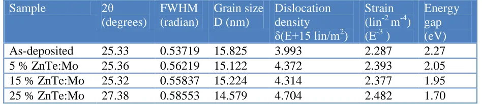
[image:4.596.62.536.533.636.2]The crystallite size (D), Strain (ԑ), dislocation density (δ) and lattice spacing are calculated and presented in Table1. As-deposited films show crystalline structure with 15.8 nm grain size. With the increase in doping concentration the grain size starts increasing. This is because more and more Mo atoms diffuses ZnTe and reduce the dislocations of ZnTe film. All the Mo atoms settle in the film dislocations and hence stress reduces with increase in doping concentrations.
Table 1. XRD analysis of ZnTe:Mo thin films
Sample 2θ
(degrees)
FWHM (radian)
Grain size D (nm)
Dislocation density δ(E+15 lin/m2
)
Strain (lin-2 m-4) (E-3 )
Energy gap (eV)
As-deposited 25.33 0.53719 15.825 3.993 2.287 2.27
5 % ZnTe:Mo 25.36 0.56219 15.122 4.372 2.393 2.05
15 % ZnTe:Mo 25.32 0.55837 15.224 4.314 2.377 1.95
25 % ZnTe:Mo 27.38 0.58553 14.579 4.704 2.482 1.70
3.2 Morphology
presence of pillar like structure is because of spherical like clusters at the surface of the annealed stack after deposition.
[image:5.596.87.522.137.362.2]Figure 2. a) As-deposited ZnTe b) 5wt% concentration of Mo, c) 15wt% concentration of Mo, d) 25% concentration of Mo
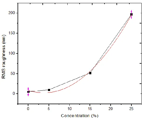
Figure 3. Surface roughness of ZnTe:Mo films for different concentrations.
[image:5.596.175.421.432.633.2]
roughness may be due to the different kinetics of the dopant atoms and the host atoms on the film surface at a particular temperature. Increasing content of Mo may increase the crystallite size and hence in the increase in the roughness of the films and hence significant modifications in the surface topographies have been observed [21, 22]. These characteristics are very well supported by the XRD results.
3.3. Optical properties
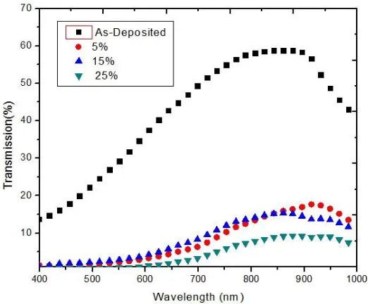
[image:6.596.172.433.364.580.2]The transmittance spectra of molybdenum doped ZnTe thin films of different concentrations are shown in fig. 4. The transmittance was found to be 50% for the undoped film compared to the doped which is from 14% to 8% at the wavelength range of 700nm to 900nm. This decrease in the transmittance is due to the increased scattering of photons by crystal defects by doping [23, 24]. Besides these, annealing is also an important factor to improve the structure of the film and to increase the grain size; it decreases the transmittance and increases absorption [25]. The optical transmittance of the film is known to depend strongly on its surface morphology [26].
Figure 4. Transmittance spectra of ZnTe:Mo films for different concentrations.
Fig 5 shows the reflectance of ZnTe:Mo thin films. It is observed that undoped ZnTe thin film has more reflectance compared to that of doped films. As the concentration increases reflectance also increases.
Figure 5. Reflectance spectra of ZnTe:Mo films for different concentrations.
The absorption was observed to be very high at shorter wavelength 500nm for doped films. As the doping concentration increased, the absorption coefficient increases with red shift in the absorption band.
Figure 6. Absorbance spectra of ZnTe:Mo films for different concentrations.
[image:7.596.166.432.399.611.2]
band into conduction band. This generates electron-hole pairs and a new charge carrier distribution is created. This effect leads to rising of forward current when light of these wavelengths in visible region is illuminated [30]
The absorption coefficient α can be calculated using the relation [31].
The fundamental absorption, which corresponds to electron excitation from the valence band to conduction band, was used to determine the nature and value of the optical energy band gap. Optical band gap was determined by the optical data with the expression for the optical absorption coefficient α and the photon energy h using the relation.
Where, k is constant
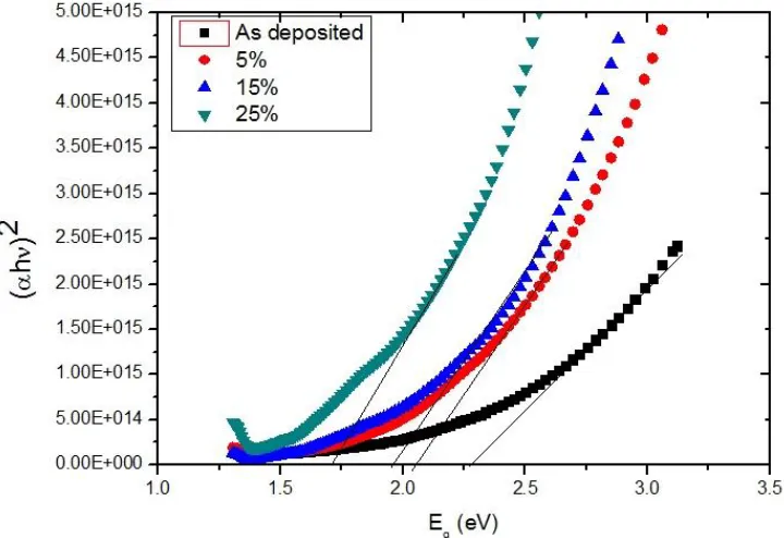
Optical energy gap of ZnTe:Mo thin films plotted for different concentration is shown in fig. 7. Here energy gap decreases with increase in Mo concentration. The narrowing of the optical band gap is due to intense doping. The values of energy gap are given in table 1. Higher Mo concentration in the films decreases the optical energy gap. This may be attributed to the band shrinkage effect because of increasing carrier concentration [32]. Similar trend of observation has been reported elsewhere for different doping materials [20, 7].
[image:8.596.112.472.471.718.2]
Figure 8. Plots of Energy gap Vs Concentration for ZnTe:Mo thin films
0 5 10 15 20 25
5.2 5.3 5.4 5.5 5.6 5.7 5.8
Z
n
T
e
:M
o
(
)
[image:9.596.169.418.99.306.2]Concentration (Mo %)
Figure 9. Calculated work function of ZnTe:Mo versus concentration
Fig 8 shows decrease in energy gap almost linearly with increase in concentration of Mo. There is a possibility of auxiliary decrease in band gap value nearly equal to zero with further increase in Mo concentration which is the evidence for decreased conduction band edge with increase in the doping concentration [20]. Optical band gap of as-deposited film was found to be 2.27 eV (theoretical 2.24 eV) whereas for 25 wt% of Mo was found to be 1.70 eV, this linear decrease can be attributed to the more number of acceptors after incorporation of Mo atoms into the ZnTe films.
[image:9.596.170.425.373.571.2]
Where, m is the metal work function, Eg is band gap of semiconductor and ‘χ’ is electron
affinity of semiconductor.
As the doping concentration changes, there is change in the work function of the semiconductor. The calculated work function with varying Mo concentration is represented in figure 9. The undoped ZnTe has maximum work function of 5.8, as the Mo concentration is increased the work function decreases linearly. Equation 7 signifies that the metal work function should be greater than the semiconductor work function ZnTe:Mo/Ni or Au [33] can be considered as a back contact for CdTe based solar cells.
4. CONCLUSIONS
ZnTe:Mo thin films were prepared using electron-beam evaporation method for different concentrations of Mo. XRD results confirmed the doping of Mo by indicating a prominent additional peak of MoTe2 for doped samples. Surface morphology indicated the presence of Mo on the surface of
ZnTe thin films. The optical transmittance decreases with increase in doping concentration in the visible region (400-800). Mo doped ZnTe showed slight increase in absorbance compared to undoped ZnTe and absorption spectrum shifts towards higher wavelength side with increase in doping concentration. Optical energy gap decreased with increase in doping concentrations due to introduction of impurity energy levels in the energy gap. It was observed that at 25wt% Mo doped ZnTe the band gap and work function is low and also the transmittance is less compared to that of undoped ZnTe. These are the prominent characteristics of a back contact. All these properties indicate that ZnTe:Mo thin films can be considered to be used for the device applications as well as back contact material for CdTe solar cells.
References
1. H. Zaari, M. Boujnah, A. El Hachimi, A. Benyoussef, A. El Kenz, Opt Quant Electron, 46 (2014) 75-86
2. M. S. Hossain, R. Islam, A. Khan, J. Optoelectronics and Advanced Materials, 9 (2007) 2192-2199
3. Mehrdad Ziari, H. Willium Steier, M. Peter Ranon, Sudhir Trivedi, B. Marvin Klein. Appl. Phys. Lett, 60 (1992) 1052
4. K. S. Akram, Aqili, Asghari Maqsood, Zulfiqar Ali, Appl. Surf. Sci, 191(2002) 280-285
5. C. Dinesh Sharma, Subodh Srivastava, Y. K. Vijay and Y. K. Sharma, Adv. Mat. Lett. 4 (2013) 68-70
6. D. N. Bose and S. Bhunia, Bull. Mater. Sci., 28 (2005) 647–650
7. K.S. Akram Aqili, J. Ahmad Saleh, Zulfiqar Ali , S. Al-Omari J. Alloys and compounds, 520 (2012) 83– 88
9. K. Makhratchev, K. J. Price, X. Ma, D.A. Simmons, J. Drayton, K. Ludwig, A. Gupta, R. G. Bohn, A. D. Compaan, Photovoltaic Specialists Conference, 2000. Conference Record of the Twenty-Eighth IEEE, (2000) 475 - 478
10.Kyu Charn Park, Eun Seok Cha, Byung Tae Ahn, Current Applied Physics, 11(2011) 109–112 11.Michael Gostein and Lawrence Dunn, Atonometrics, Inc. Austin, Texas 78757 prepared for NREL
PV Module Reliability Workshop (2011)
12.H. Samuel Demtsu, Impact of back-contact materials on performance and stability of CdS / CdTe Solar cells, (2006)
13.M. S. Hossain, R. Islam, K. A. Khan, J. Ovonic Research, 5 (2009) 195-205
14.Lim Yei Ying, Nor Hamizah Bt. Mazlan and T. Joseph Sahaya Anand, United Kingdom – Malaysia – Ireland, Engineering Science Conference, (2011)
15.M. Becerril, O. Vigil-Galán, G. Contreras-Puente, O. Zelaya-Angel, Revista mexicana de física, 57 (2011) 304–308
16.G. K. Paul, S Bandyopadhyay, S. K. Sen and S. Sen, Mater. Chem. Phys., 79 (2003) 71-75.
17.A. Tiburcio-Silver, A. Sanchez-Juarez and A. Avila-Garcia, Sol. Energy Mater. Sol. Cells, 55 (1998) 3-10
18.Ming Luo, Transition-Metal Ions in II-VI Semiconductors : Zinc Selenide and Zinc Telluride, West Virginia University (2006)
19.Greg Sun, Physics 621: Physics of Semiconductor Materials, Applied Physics Graduate Program, (2008)
20.Jayadev Pattar, N. Shilpa Sawant, M. Nagaraja, N. Shashank, K. M. Balakrishna, Ganesh Sanjeev and H. M. Mahesh, Int. J. Electrochem. Sci., 4 (2009) 369-376.
21.K. Muthukkumaran, P. Kuppusami, T. Mathews, E. Mohandas, S. Selladurai, Materials Science-Poland, 25 (2007) 671-678.
22.Ali Jasim AL-Jabiry, Al- Mustansiriyah J. Sci. 23 (2012) 173-182
23.Fatema Rezwana Chowdhury, Shahima Choudhury, Firoz Hasan and Tahmina Begum, J. Bangladesh Academy of Sciences, 35 (2011) 99-111
24.P. K. Manoj, Benny Joseph, V. K. Vaidyan, D. Sumangala Devi Amma, Ceramics International , 33 (2007) 273–278
25.M. Eman Abid, Dr. M. Inaam Abdul Majeed, Dr. A. Kadhim Aadim, Int J. Innovative Research in Science, Engineering and Technology, 2 (2013)
26.T. Prasada Rao, M. C. Santhosh Kumar, J. Crystallization Process and Technology, 2 (2012) 72-79 27.D. Paul Joseph and C. Venkateswaran, J. Atomic, Molecular, and Optical Physics, 2011 (2011),
Article ID 270540
28.Kwang Joo Kim and Young Ran Park, J. Appl. Phys., 96 (2004) 4150
29.S. A. Yousaf and S. Ali, PK ISSN 0022- 2941; CODEN JNSMAC, 48 (2008) 43-50 30.P. Nollet, M. Burgelman, S. Degrave, Thin Solid Films, 361-362 (2000) 293-297
31.R. S. Meshram, R. M. Thombre and B. M. Suryavanshi, Advances in Applied Science Research, 2012, 3 (3):1271-1278
32.Min Su Kim, Kwang Gug Yim, Jeong-Sik Son and Jae-Young Leem, Bull. Korean Chem. Soc. 33 (2012) 1235
33.N. R. Paudel, A. D. Compaan, and Y. Yan, Solar Energy Materials and Solar Cells, 113 (2013) 26– 30.