This is a repository copy of
The need for macro-models in the simulation of EMI effects in
integrated circuits
.
White Rose Research Online URL for this paper:
http://eprints.whiterose.ac.uk/84202/
Version: Submitted Version
Proceedings Paper:
Dawson, J.F. orcid.org/0000-0003-4537-9977, Persyn, W., Hagiwara, S. et al. (1 more
author) (1994) The need for macro-models in the simulation of EMI effects in integrated
circuits. In: EMC'94 Roma. , Rome, Italy , pp. 638-643.
[email protected]
https://eprints.whiterose.ac.uk/
Reuse
Items deposited in White Rose Research Online are protected by copyright, with all rights reserved unless
indicated otherwise. They may be downloaded and/or printed for private study, or other acts as permitted by
national copyright laws. The publisher or other rights holders may allow further reproduction and re-use of
the full text version. This is indicated by the licence information on the White Rose Research Online record
for the item.
Takedown
If you consider content in White Rose Research Online to be in breach of UK law, please notify us by
THE NEED FOR MACRO–MODELS IN THE SIMULATION
OF EMI EFFECTS IN INTEGRATED CIRCUITS
J.F. Dawson
†
, J. Wood
†
, W. Persyn
‡
, and S. Hagiwara
†
†Department of Electronics ‡Department of Electronics
University of York Katholieke Industriele Hogeschool
Heslington West-Vlaanderen (KIHWV)
York YO1 5DD Oostende
England Belgium
Abstract
The paper briefly reviews the previous work on the simulation of EMI effects in integrated circuits. Both component level and macro-models are considered. The relative merits of component level models and macro-models for EMI effects are discussed. In particular the problem of obtaining accurate data for component level models and the possibility of obtaining macro-model parameters by measurement are considered. The need to consider the coupling between all terminals is discussed. This contrasts with previous published work where only input to output effects are presented. Results are presented for some simple CMOS amplifier circuits.
I Introduction
Computer simulation of the performance of an ICL8741 operational amplifier was first described by Wooley & Wong in 1971 [1]. This paper provides an insight into the detail and complexity of simulating a subsystem which is so common that we now take if for granted. Among the programs used for this simulation was CANCER (Computer analysis of non-linear circuits excluding radiation), from which the SPICE (Simulation program with integrated circuit emphasis) family of simulators was developed by the University of California, Berkeley in the mid–1970s. Tuinenga’s book [13] provides an excellent introduction to the history and capabilities of the SPICE family of circuit simulators though its emphasis is on the commercial package PSPICE.
The complexity of fully modelling each of the devices within a simple circuit, such as a logic gate or operational amplifier, caused the search for simplified models capable of accurately representing the overall function of a circuit to follow closely after the development of the first circuit simulators. The ICL8741 was again the first chip to feature in the literature with a simplified macro–model described by Boyle et al [2]. The macro–model reduced the computation time for simple op-amp circuits by a factor of six whilst producing results which were very close to the full model. The ideas of Boyle et al have been developed by a number of other workers [3], [4], & [5]. Macro models based on this work are widely available for modern operational amplifiers, often supplied by the IC manufacturers. An excellent overview of the technique is given in [6], which also suggests a number of developments to improve the performance of the macro–models.
As well as the reduction in complexity, the use of macro–models has the major advantage that detailed knowledge of the chip fabrication parameters is not required — the macro–model parameters can be determined easily from the manufacturers data sheet. This allows the chip manufacturers to keep their commercially sensitive fabrication data secret whilst providing the user with a model which is accurate for the specified operating range of the chip. However many macro–models do not accurately reproduce the operation of an integrated circuit outside its normal operating range or for power supply currents.
Modelling of the effects of electromagnetic interference on electronic circuits was first described by Larson & Roe [7] who developed a modified Ebers–Moll transistor model to allow the demodulation effect due to the non-linearity of a bipolar transistor junction to be simply modelled in circuit simula-tions. The essence of the model was to introduce a dc current into the transistor proportional to the incident rf power. The rf signal does not need to be simulated, greatly reducing the simulation time. However the model is only appropriate where a single frequency interference is present and could not be used for transient effects. This transistor model was used by Tront, Whalen et al [8] to develop an EMI macro–model for the 741 op-amp. Other macro-models of the 741 op–amp have been developed ([10, 11]) which use full transistor simulations for the input stage, where most of the non-linear effects occur, whilst using ideal circuit elements (e.g. dependent voltage sources) for the remainder of the amplifying stages.
C C C In+ In-L M8 M5 M9 M10 M6 M7 M1 M4 M3 M2 OPAMP2 VDD 14 44 2 52 1 48 43 55 11 30 8 IBIAS VBIAS
Figure 1: The op-amp circuit showing node numbers
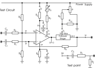
C C FBias OP-O OP-F R R R R R R R R R P R R J J J J J TP TP TP TP TP TP V X X X X X TPX X 1 1 1 2 2 2 3 3 4 4 5 5 6 7 8 9 10 + Vin Vin _ Follower Stage VDD VSS Bias Power Supply Test Circuit C TP X Ri Rj tp 1 Test point
Figure 2: Test circuit for the op-amp showing the output source follower stage as a separate block, and current monitoring links. The EMI injection circuit (test point) is shown separately.
The published EMI macro–models concentrate on mimicking the demodulation effects of EMI at the input terminals of a 741 (or similar) op-amp. However EMI may enter through any terminal and macro–models are required which will accurately mimic the complete circuit behaviour. Work is currently being carried out at the University of York, in collaboration with KIHWV to develop full macro–models which mimic the interaction of EMI between all terminals.
A significant entry point for EMI is via the power supply rails of a circuit. It is in this area that this paper presents some results.
The work described above and the remainder of this paper considers only interference entering the chip from outside via the circuit connections. This approach is valid for many applications because the small physical size of the chip means that direct pick-up by the chip itself is negligible.
II The CMOS Integrated Circuits
A CMOS integrated circuit fabricated as part of a student project at the Katholieke Industriele Hogeschool West-Vlaanderen (KIHWV), Belgium, is used for the work carried out in this study because the detailed device parameters are available. On the chip are fabricated two op-amps, and two operational transconductance amplifiers (OTAs). The two op-amps use the same circuit configuration but different transistor geometries; as do the two OTAs.
The op-amp circuit is shown in Figure 1. The input stage is a differential amplifier input stage (M1 & M2) with current mirror active loads (M3 & M4). This is followed by a common source stage (M5) with a constant current active load (M6). A source follower output stage (M9) is used with a constant current load (M10). The bias current for the differential amplifier and common source stages are supplied via the current mirror circuit M6, M7, and M8. The current in M8 is set by an external bias circuit and controls the current in M6 and M7. The current in the output stage is set by the gate bias voltage applied to M10. Closed loop stability is ensured by the on-chip miller capacitance Cc.
The test chip is encapsulated in a 40-pin dual in-line package with each circuit having separate power supply and ground connections.
III The test circuit
[image:3.595.73.272.185.327.2]ICF
CIN
VIN
-VIN+
R1
R2
VCM ISS
R3 C1 R4
EOS
G2VA
G1VA
R7
R8
C2
C3
R9
R10
VA
VB
VDD
VSS
[image:4.595.70.279.15.145.2]VF
Figure 3: PMI Macro–model (input circuit).
D5 D6
D3
D4
VF
D7 D8
G13 G14
V3
V4
G11
G12
R23
L5
R24
VDD
VSS
[image:4.595.80.278.182.297.2]Out
Figure 4: PMI Macro–model (output stage).
circuit board with one side dedicated to a continuous ground plane. The presence of a ground plane provides well defined parasitic capacitances for the circuit board and minimises inter-track coupling. Test points were included to allow radio-frequency interference to be injected at any pin of the IC with minimal effect on normal circuit operation. Current monitoring jacks (J2 and J5) were also provided to allow the circuit quiescent conditions to be set accurately.
IV The Macro–model
The enhanced Boyle macro–model of Alexander and Bowers of Precision Monolithics Inc. (PMI) [6] is used to determine the low frequency performance of the amplifier. This is shown in Figures 3, 4, and 5. The input stage is simplified version of the real op–amp. Subsequent stages using voltage controlled current sources (VCCSs) allow the frequency response of the amplifier to be set with an arbitrary degree of accuracy.
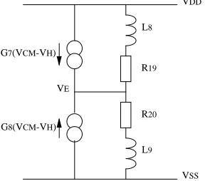
The output stage also uses a number of VCCSs (Figure 4) with diodes to limit the output voltage swing and to provide output current limiting. The common mode gain and frequency response is set independently by further VCCSs (Figure 5). The voltage,VE generated by the common mode circuit
is scaled and added to the input offset voltage source in Figure 3. This part of the model can easily be created directly from the manufacturer’s data sheet for any op-amp.
G7(VCM-VH)
G8(VCM-VH)
L8
L9
R19
R20
VSS
VDD
VE
[image:4.595.86.230.563.690.2]VIN+
VCVS
CIN1+ DIN1+
RIN1+ RIN2+ CIN2+
Eos
Figure 6: Addition to the PMI Macro–model to model demodulation effects at each input of the op–amp.
In order to model the demodulation effects in the op–amp a separate circuit can be included (Figure 6). The ac coupled input waveform is directly rectified and a scaled version fed to the offset voltage source in Figure 3. Though a simple frequency independent network has been used here, it would be straightforward to add a frequency dependent network to cause the demodulation to have a variation with frequency. A polynomial source could be used to model the real non-linearity more closely.
In order to model coupling from the power supply pin to the output of the op-amp a frequency dependent network was developed (Figure 7) which mimics the small signal response of the full circuit model. An additional non–linear network (currently of the same form as Figure 3) is used to account for additional demodulation effects in this coupling path. These networks control a current source (GDD) which acts in parallel with those in the output stage (4).
VDD
RDD1
Control
of GDD
GDDin CDD0 RDD0
CDD2
GDD1
RDD2
LDD2
[image:5.595.70.282.257.392.2]GDD1
Figure 7: Addition to the PMI Macro–model to mimic coupling from Vdd to the output of the op–amp.
V Results
V.1 Frequency response
-100 -80 -60 -40 -20 0 20
100 1000 10000 100000 1e+06 1e+07 1e+08
Gain (dB)
Frequency (Hz) Inverting input to output
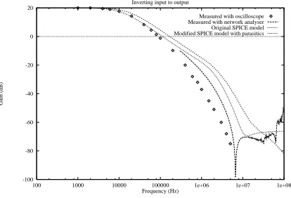
[image:5.595.192.399.483.624.2]Measured with oscilloscope Measured with network analyser Original SPICE model Modified SPICE model with parasitics
Figure 8: Frequency response of op-amp circuit – computed (full circuit models) and measured.
-200 -150 -100 -50 0 50 100 150 200
100 1000 10000 100000 1e+06 1e+07 1e+08
Phase (deg.) 0,0
Frequency (Hz) Inverting input to output
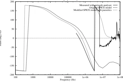
[image:6.595.192.399.11.148.2]Measured with network analyser Original SPICE model Modified SPICE model with parasitics
Figure 9: Phase response of op-amp circuit – computed (full circuit models) and measured.
The measured and computed (SPICE full circuit model) frequency and phase responses of the op-amp, inverting input (non-inverting open circuit) are shown in Figures 8 and 9. It can be seen that the measured and computed responses begin to diverge at 1 MHz. The addition of the parasitic capacitances around the circuit improves matters to some extent but there is still a significant dif-ference between computed and measured curves. The parasitic capacitances of each track to ground (2 pF approx.) affect the frequency response around 1 MHz whilst a very small coupling capacitance (0.01 pF) between input and output connections causes the leveling of the frequency response above 10 MHz.
-100 -80 -60 -40 -20 0 20
100 1000 10000 100000 1e+06 1e+07 1e+08
Gain (dB)
Frequency (Hz) Inverting input to output
[image:6.595.190.399.281.419.2]Original SPICE model SPICE model with parasitics PMI Macro-model with parasitics
Figure 10: Comparing the amplitude response of the PMU Macro–model with the full (SPICE) circuit models.
-200 -150 -100 -50 0 50 100 150 200
100 1000 10000 100000 1e+06 1e+07 1e+08
Phase (deg.)
Frequency (Hz) Inverting input to output
[image:6.595.191.400.467.605.2]Original SPICE model SPICE model with parasitics PMI Macro-model with parasitics
Figure 11: Comparing the phase response of the PMI Macro–model with the full circuit models.
-70 -60 -50 -40 -30 -20 -10 0 10
100 1000 10000 100000 1e+06 1e+07 1e+08
Gain (dB)
Frequency (Hz) Vdd to output
[image:7.595.189.397.7.150.2]Spice model with parasitics PMI model PMI model with EMI effects
Figure 12: Comparing amplitude response Macro–models with the full circuit models.
-120 -100 -80 -60 -40 -20 0 20 40 60 80 100
100 1000 10000 100000 1e+06 1e+07 1e+08
Gain (dB)
Frequency (Hz) Vdd to output
[image:7.595.192.402.186.322.2]Spice model with parasitics PMI model PMI model with EMI effects
Figure 13: Comparing the phase response of the Macro–models with the full circuit models.
V.2 Time response
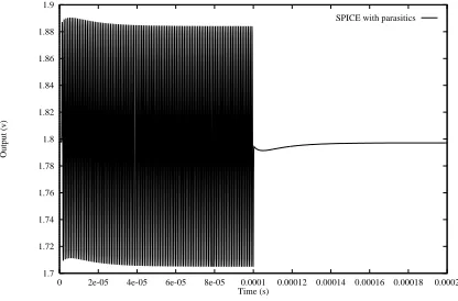
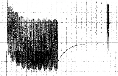
In order to observe the demodulation effects a short burst of 1 MHz sine–wave was injected into the Vdd rail and the output observed. Figure 14 shows the response of the full circuit SPICE model, and 15 shows the response of the EMI enhanced PMI macro-model. It can be seen that the major effect is carrier feedthrough. A small low–frequency disturbance can be seen near the start of each burst. This is due in part to the non-linearity in the path from Vdd to the output and partly to the non–linear response of the the input circuit to energy from the pulse coupled via other circuit elements (the separate effects can be observed if parts of the PMI model are selectively disabled). The PMI model was tuned to match the full–circuit SPICE model, however when measurements were carried out the real circuit showed a smaller carrier feedthrough and a larger non–linear effect (Figure 16). The PMI macro model can easily modified to follow this as is shown in Figure 17.
1.7 1.72 1.74 1.76 1.78 1.8 1.82 1.84 1.86 1.88 1.9
0 2e-05 4e-05 6e-05 8e-05 0.0001 0.00012 0.00014 0.00016 0.00018 0.0002
Output (v)
Time (s)
SPICE with parasitics
[image:7.595.191.399.506.643.2]1.7 1.72 1.74 1.76 1.78 1.8 1.82 1.84 1.86 1.88 1.9
0 2e-05 4e-05 6e-05 8e-05 0.0001 0.00012 0.00014 0.00016 0.00018 0.0002
Output (v)
Time (s)
[image:8.595.190.397.10.148.2]PMI Macro-Model
[image:8.595.196.394.192.320.2]Figure 15: Amplitude response of the PMI Macro–models with 0.2Vpp 1 MHz tone burst on Vdd rail.
Figure 16: Measured response of op-amp circuit to 0.2Vpp 1 MHz tone burst on Vdd rail (scale: 20 µs,
20 mV per div).
VI Conclusions
The paper has suggested some ideas for further developing EMI macro–models for operational amplifier circuits. It is important that all terminals are considered if the effect of EMI on electronic circuits is to be modelled. The ingress of EMI via the power rails (and other terminals) is a topic which must be addressed if susceptibility modelling of circuits is to be possible.
The particular macro–models suggested are intended to demonstrate some possibilities. Further work must be carried out to optimise the models and determine the degree of accuracy required.
The work presented has shown results for small signal coupling, and non-linear effects in limited circumstances. If EMI macro–models are to be used effectively further work must be carried out to determine the measurements required to develop an adequate model.
1.72 1.74 1.76 1.78 1.8 1.82 1.84 1.86 1.88 1.9
0 2e-05 4e-05 6e-05 8e-05 0.0001 0.00012 0.00014 0.00016 0.00018 0.0002
Output (v)
Time (s)
’ckt4/tdxqgm3d.tds’
Figure 17: Amplitude response of the PMI Macro–model with 0.2 Vpp 1 MHz tone burst on Vdd rail:
[image:8.595.191.399.519.658.2]VII Acknowledgements
Thanks are due to:
• DRA Malvern for funding some of this work.
• Prof. J Catrysse of the Katholieke Industriele Hogeschool West-Vlaanderen (KIHWV), Belgium,
for the loan of the ICs used in this work.
References
[1] B. A. Wooley, S. J. Wong, & D. O. Pederson,A computer aided evaluation of the 741 amplifier, IEEE J. Solid-state Circuits, Vol. SC–6, No. 6, pp. 357–366 Dec. 1971
[2] G. R. Boyle, B. M. Cohn, D. O. Pederson, & J. E. Solomon ,Macromodeling of integrated circuit operational amplifiers, IEEE J. Solid-state Circuits, Vol. SC–9, No. 6, pp. 353–363 Dec. 1974 [3] G. Krajewska, & F. E. Holmes,Macromodeling of FET/Bipolar operational amplifiers, IEEE J.
Solid-state Circuits, Vol. SC–14, No. 6, pp. 1083–1087, Dec. 1979
[4] C. Turchetti, & G. Masetti, A macromodel for all–MOS operational amplifiers, IEEE J. Solid-state Circuits, Vol. SC–18, No. 4, pp. 389–394, Aug. 1983
[5] B. Perez–Verdu, J. L. Huertas, & A. Rodriguez–Vazquez,A new nonlinear time-domain op-amp macromodel using threshold functions and digitally controlled network elements, IEEE J. Solid-state Circuits, Vol. 23, No. 4, pp. 959–971 Aug. 1988
[6] M. Alexander & D. F. Bowers,SPICE compatible op–amp macro–models, Precision Monolithics, Application note 138, reprinted from EDN, Feb. 15th & Mar. 1, 1990.
[7] C. E. Larson & J. M. Roe,A modified Ebers-Moll Transistor model for RF–interference analysis, IEEE Trans on EMC, Vol. EMC–21, No. 4, pp. 283–290, Nov. 1979
[8] J. G. Tront, J. J. Whalen, C. E. Larson & J. M. Roe,Computer–aided analysis of RFI effects in operational amplifiers, IEEE Trans on EMC, Vol. EMC–21, No. 4, pp. 297–306, Nov. 1979 [9] P. R. Gray & R. G. Meyer,MOS operational amplifiers design — A tutorial overview, IEEE J.
Solid-state Circuits, Vol. SC-17, No. 6, pp.969–981 Dec. 1982
[10] S. Graffi, G. Masetti, & D. Golzio,New macromodels and measurements for the analysis of EMI effects in 741 op–amp circuits, IEEE Trans on EMC, Vol. 33, No. 1, pp. 25–34, Feb. 1991 [11] D. Golzio, S. Graffi, Zs. M. V. Kovacs, G. Masetti, Opamp macromodel design techniques for
EMI simulation, 10th Int. Zurich Symposium on EMC, 9–11 March, 1993, pp. 207–212
[12] H. Naert & A. Nissenne,Analoog ontwerp met behulp van symbolisch layout–programma, project report, Dept. of Electronics, Katholieke Industriele Hogeschool West-Vlaanderen, 1987
[13] Paul W Tuinenga, 1992,SPICE A guide to circuit simulation and analysis using PSPICE, 2nd Edition, Prentice Hall