This is a repository copy of
GeSn lasers for CMOS integration
.
White Rose Research Online URL for this paper:
http://eprints.whiterose.ac.uk/113233/
Version: Accepted Version
Proceedings Paper:
Buca, D, von den Driesch, N, Stange, D et al. (9 more authors) (2017) GeSn lasers for
CMOS integration. In: Electron Devices Meeting (IEDM), 2016 IEEE International. IEEE
International Electron Devices Meeting (IEDM), 03-07 Dec 2016, San Francisco, USA.
IEEE , pp. 588-591. ISBN 978-1-5090-3902-9
https://doi.org/10.1109/IEDM.2016.7838472
© 2016, IEEE. This is an author produced version of a paper published in Electron Devices
Meeting (IEDM), 2016 IEEE International. Personal use of this material is permitted.
Permission from IEEE must be obtained for all other users, including reprinting/
republishing this material for advertising or promotional purposes, creating new collective
works for resale or redistribution to servers or lists, or reuse of any copyrighted
components of this work in other works. Uploaded in accordance with the publisher’s
self-archiving policy.
[email protected] https://eprints.whiterose.ac.uk/
Reuse
Unless indicated otherwise, fulltext items are protected by copyright with all rights reserved. The copyright exception in section 29 of the Copyright, Designs and Patents Act 1988 allows the making of a single copy solely for the purpose of non-commercial research or private study within the limits of fair dealing. The publisher or other rights-holder may allow further reproduction and re-use of this version - refer to the White Rose Research Online record for this item. Where records identify the publisher as the copyright holder, users can verify any specific terms of use on the publisher’s website.
Takedown
If you consider content in White Rose Research Online to be in breach of UK law, please notify us by
GeSn Lasers for CMOS Integration
D. Buca
1, N. von den Driesch
1, D. Stange
1, S. Wirths
1, R. Geiger
2, C. Schulte Braucks
1, S. Mantl
1, J.M. Hartmann
3, Z.
Ikonic
4, J. Witzens
5, H. Sigg
2, D. Grützmacher
11 Peter Grünberg Institute 9, Forschungszentrum Jülich GmbH, Jülich, Germany
2Laboratory for Micro- and Nanotechnology (LMN), Paul Scherrer Institute, CH-5232 Villigen, Switzerland 3CEA, LETI, MINATEC Campus and Université Grenoble Alpes, F-38054 Grenoble, France 4Institute of Microwaves and Photonics, University of Leeds, Leeds LS2 9JT, United Kingdom
4Institute of Integrated Photonics, RWTH Aachen, 52074 Aachen, Germany
E-mail: [email protected]
Abstract - In search of a suitable CMOS compatible light source
many routes and materials are under investigation. Si-based group IV (Si)GeSn alloys offer a tunable bandgap from indirect to direct, making them ideal candidates for on-chip photonics and nano-electronics. An overview of recent achievements in material growth and device development will be given. Optically pumped waveguide and microdisk structures with different strain and various Sn concentrations provided direct evidence of gain in these alloys and of the width of the emission wavelength range that can be covered. With the final aim being the fabrication of electrically pumped lasers, a set of different homo-junction light emitting diodes and more complex heterostructure SiGeSn/GeSn LEDs is presented. Detailed investigations of electroluminescence spectra indicate that GeSn/SiGeSn heterostructures will be advantageous for future laser fabrication.
I. INTRODUCTION
Since 2016, the semiconductor industry research plan is no longer primarily centered on Moore’s law, i.e., on improving chip performance first and then focusing on applications. Thus, the integration of additional, value-added functionalities on future silicon dies will be key for upcoming strategies, which will start with the application defining the functionality of chips. This will require the integration of a large variety of devices such as amplifiers, ultra-low power switches and optoelectronic devices on the very same Si substrate. In this respect, silicon/group IV Photonics promises to reduce the power consumption of electric circuits through the addition of optical components. In order to transfer electrically stored information to an optical circuit, an on-chip laser is highly desireable. Enormous effort has been spent on the development of III-V growth on Si or alternative solutions for the integration into CMOS processing. However, group IV materials such as Ge and (Si)GeSn offer a promising perspective for CMOS integration and represent possible candidates for light emission in the SWIR-NIR range. In the past few years, the epitaxy of GeSn and SiGeSn alloys has improved dramatically. As a result, industry-compatible epitaxial reactors for wafer sizes of 200-300 mm can be used nowadays, indicating the enormous potential of these alloys for large-scale optoelectronic integration.
II. GESN LASERS
For the presented laser experiments, GeSn epilayers of up to 800 nm thickness (Fig.1), with Sn concentrations ranging between 8.5-14 at.% [1], were grown on 2.5 m thick Ge buffers employing reactive gas phase epitaxy and growth temperatures below 400°C. Subsequently, Fabry-Pérot and microdisk laser cavities were formed using Si CMOS compatible processing, as shown in Fig. 2. GeSn mesas were anisotropically dry-etched using Cl2/Ar reactive ion etching. Parts of the waveguides were
selectively underetched, up to approx. 4 m undercut, with CF4
chemistry. All samples were passivated using Al2O3. This step is
especially important in order to reduce the surface recombination of carriers. It is shown schematically in Fig. 3 for non-underetched Fabry-Pérot waveguides. The Al2O3 passivated
cavities show a much lower temperature dependence of lasing threshold. The unsaturated surface states induce a temperature dependent carrier density associated with a decrease of the non-radiative lifetime (Fig. 4). The lasing characteristics, however, indicate that, at 20 K, the threshold is not limited by surface recombinations.
The underetching of cavities, as shown in Fig. 5a, improves the device performance in terms of optical mode overlap and strain relaxation; due to the higher refractive index difference between GeSn and the surrounding air, the mode overlap with the direct bandgap GeSn material increases from 60% to about 100%, as shown in the inset of Fig. 5a. On the other hand, (compressive) strain relaxation in the layer enlarges the so-called directness, defined as the energy difference between the indirect L- and direct -valleys. Waveguides with a width of 10 m show a directness of about 15 meV, which can be improved to > 30
meV by underetching the cavity by 3.6 m, as simulations
indicate (cf. Fig. 5b). As a consequence, the higher carrier density in the direct valley, available for radiative recombination, leads to an improved lasing performance.
from approx. 430 kW/cm2 to 206 kW/cm2 for the undercut cavity
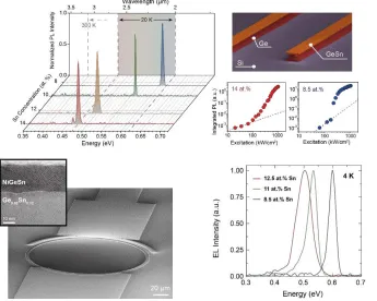
and the slope efficiency of the laser is more than doubled in underetched waveguides (x2.2). Additionally, the temperature range of operation is extended in underetched devices. While lasing originally vanishes at temperatures above ~90 K, underetched structures show lasing up to 135 K, despite the reduced capacity for excess heat dissipation in this type of structures. We attribute the improved performance to the increased directness of the material. Similar results are also obtained for micro-disk GeSn cavities (Fig. 7). The high resolution spectra of the whispering gallery laser modes are shown in Fig 8.
The emission of the GeSn lasers can be tuned to cover a broader range of the SWIR spectrum. Along with strain engineering, Sn incorporation strongly influences the emission wavelength. Fig. 9 presents the measured laser emission at 20 K, between 2µm and 2.6 m for Sn contents of 8.5, 10, 12.5 and 14 at.%. If room temperature lasing is obtained, the available range should come
up to 3 m, due to temperature-related bandgap narrowing.
III. GESN-BASED LIGHT EMITTING DIODES
On the road to an electrically pumped GeSn laser, the electroluminescence is first studied in GeSn light emitting diodes (LEDs). The complete p-i-n layer stack is grown in-situ on relaxed GeSn buffers. GeSn homo-junctions with Sn contents between 8.5 and 12.5 at.% were processed using standard CMOS technologies. The mesa and the contact areas are defined by optical lithography and reactive ion etching (Cl2/Ar plasma)
followed by an Al2O3/SiO2 passivation. Finally, ~20 nm thick
stanogermanide contacts [4] are formed. Figure 10 shows an SEM image of a processed LED. Light emitting diodes are characterized by pulsed bias EL measurements with a duty cycle of 50%. Three homo-junction GeSn LEDs with diameters of 100 µm are compared and the spectra at 4 K shown in Fig. 11. The emission peak energy is blue-shifted from 0.5 eV up to 0.6 eV with decreasing Sn concentration due to the corresponding increase of the bandgap. Similar to PL experiments [5] the temperature dependent EL spectra (Fig. 12) of Ge0.92Sn0.08 diodes are typical for indirect semiconductors,
whereas band structure calculations reveal that the Ge0.89Sn0.11
diodes are at the indirect-to-direct bandgap transition, which is verified experimentally by a steady EL increase with decreasing temperature (cf. Fig. 12).
Increase of EL can be obtained via carrier confinement in
multi-quantum-well (MQW) heterostructure LEDs.
Ge0.9115Sn0.085 as an active material and Ge or SiGeSn (with
10.5 at.% Si and 11 at.% Sn) as barriers were used in such stacks (Fig. 13a). In these ternary alloys, the band alignments allow more efficient carrier injection. MQWs were pseudomorphically grown on partially relaxed Ge0.915Sn0.085 buffers with different
thicknesses. The residual compressive strain of the GeSn/strained Ge (20 mn/14 nm) and of the GeSn/SiGeSn (19nm/11nm) structures amount to -0.71% to -0.2%, respectively. The strain induced shift of the energy bands causes a red-shift of the emission energy of the GeSn/SiGeSn MQW (Fig. 13). A clear increase of the emitted light intensity is observed for GeSn/SiGeSn MQW devices, which is attributed to the increased directness of the sample and predominantly to an improved
carrier confinement in the well. Figure 13b and c show the calculated band structure of MQWs with Ge and SiGeSn as barrier materials, respectively. In contrast to the band alignment with Ge barriers, the GeSn/SiGeSn configuration offers a clear Type-I band alignment, confining both electrons and holes inside the well. Holes of the GeSn/Ge structure are more confined in the barrier than in the well [6]. In the GeSn/Ge structure the holes actually pile up in the barrier, rather than in the well layers. Intensities integrated over the whole temperature range and normalized to the room temperature signals are provided in Fig. 14. The measurement again confirms the superior performance of GeSn/SiGeSn MQWs compared to GeSn/Ge MQWs: at RT, the EL increase is about 6x and about 20x at 20K. In the used setup a minimum injection current density of 20 mA/cm2 was
necessary to detect EL. Duty cycle and power dependent measurements were also performed on the GeSn/SiGeSn MQW LEDs. The emission peak position is tracked to identify possible heating effects, which could result in a decreased emission energy. Results are presented in Fig. 15. Increasing the peak current density leads to band filling for low injection current densities while, above 100 Acm-2, the emission energy remains
constant. Also, increasing the duty cycle does not change the emission energy, indicating that heating effects do not influence the measured results.
Conclusion
We have shown that direct bandgap GeSn is a promising optical material for Si-based laser fabrication. Four optically pumped GeSn lasers with different Sn content, and with two different laser cavities were demonstrated at low temperature. With electrically pumped lasers being the final target, type I SiGeSn/GeSn MQW LED were successfully tested, showing operation with injection currents as low as 10 mA at 20K and 50 mA at 300K. Investigations of Fabry-Pérot laser cavities using such advanced Sn based MQW layers are in progress.
REFERENCES
[1] N. von den Driesch, D. Stange, S. Wirths, G. Mussler, B. Holländer, Z. Ikonic, J. M. Hartmann, T. Stoica, S. Mantl, D. Grützmacher, and D.
Buca, “Direct Bandgap Group IV Epitaxy on Si for Laser Applications,”
Chem. Mater., vol. 27, no. 13, pp. 4693–4702, Jun. 2015.
[2] S. Wirths, R. Geiger, N. von den Driesch, G. Mussler, T. Stoica, S. Mantl, Z. Ikonic, M. Luysberg, S. Chiussi, J. M. Hartmann, H. Sigg, J. Faist, D.
Buca, and D. Grützmacher, “Lasing in direct-bandgap GeSn alloy grown
on Si,” Nat. Photonics, vol. 9, no. January, pp. 88–92, Jan. 2015. [3] D. Stange, S. Wirths, R. Geiger, C. Schulte-Braucks, B. Marzban, N. von
den Driesch, G. Mussler, T. Zabel, T. Stoica, J.-M. Hartmann, S. Mantl,
Z. Ikonic, D. Grützmacher, H. Sigg, J. Witzens, and D. Buca, “Optically
pumped GeSn Microdisk Lasers on Si,” ACS Photonics, vol. 3, No. 7, p. 1279-1285, Jun. 2016.
[4] S. Wirths, R. Troitsch, G. Mussler, J.-M. Hartmann, P. Zaumseil, T.
Schroeder, S. Mantl, and D. Buca, “Ternary and quaternary Ni(Si)Ge(Sn)
contact formation for highly strained Ge p- and n-MOSFETs,” Semicond. Sci. Technol., vol. 30, no. 5, p. 055003, May 2015.
[5] D. Stange, S. Wirths, N. von den Driesch, G. Mussler, T. Stoica, Z. Ikonic, J. M. Hartmann, S. Mantl, D. Grützmacher, and D. Buca, “Optical transitions in direct-bandgap Ge1–x Snx alloys,” ACS Photonics, vol. 2, no. 11, pp. 1539–1545, Nov. 2015.
[6] D. Stange, N. von den Driesch, D. Rainko, C. Schulte-Braucks, S. Wirths, G. Mussler, A. T. Tiedemann, T. Stoica, J. M. Hartmann, Z. Ikonic, S.
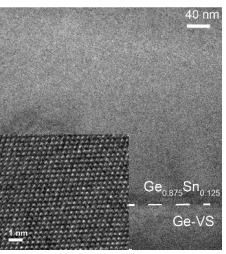
Fig. 1: Cross-section Transmission Electron Mircoscopy image showing high quality Ge0.875Sn0.125 with a thickness of 414 nm.
Fig. 2: Fabrication of Fabry-Pérot lasers by GeSn waveguide patterning and Al2O3 passivation, (a-b);
Fig. 3: Light in - light out characteristics for (a) as processed and (b) Al2O3 passivated Ge0.875Sn0.125 waveguide cavity lasers.
Fig. 4: Temperature dependence of the laser threshold for passivated and unpassivated waveguide cavities.
Fig. 5. Underetched WG structures (a) show a high optical mode overlap (inset) and an improved band structure directness EL-E (b).
[image:4.612.104.217.53.180.2]Fig.7: Underetched GeSn microdisk cavity.
Fig. 6: L-L plot for undercut (red) and non-undercut (blue) Ge0.875Sn0.125 cavities at 20 K (a) and the corresponding normalized edge emission spectra (b)
Fig. 8: High resolution laser spectra for GeSn microdisks
Al2O3
b)
[image:4.612.255.529.58.173.2] [image:4.612.76.541.210.705.2] [image:4.612.80.526.229.349.2] [image:4.612.75.397.403.507.2]Fig. 9. Low temperature laser wavelength tuning from 2 up to
the Sn content
from 8% up to 14%. Note that the GeSn layers exhibit some residual compressive strain.
Fig. 10. 3D SEM image of a processed LED structure. Inset: TEM micrograph of the resulting NiGeSn contact.
Fig. 11. Homojunction LEDs with different Sn contents show a shift in low temperature EL emission peak.
Fig. 12. Temp. evolution of the
integrated EL for two
homojunction LEDs
Fig. 14: Temperature dependent EL emission trend for MQW LEDs with different barrier types.
Fig. 13. a) Comparison of room temperature EL of GeSn-based MQW LEDs and band structures with either b) Ge or c) SiGeSn barriers.
[image:5.612.77.422.64.340.2] [image:5.612.71.555.78.686.2] [image:5.612.78.375.407.649.2]