International Journal of Innovative Technology and Exploring Engineering (IJITEE) ISSN: 2278-3075, Volume-8 Issue-9, July 2019
Abstract: In this paper, we have proposed the development of the Enhanced 8-bit RISC architecture and the temporal performance analysis of the enhanced architecture. The enhanced 8 bit RISC architecture is powered with the additional block called as Co-operative Arithmetic and Logical Unit (CALU). The 8 bit core is designed using FPGA as SPARTAN-6 XC65LX9-3TQG144. The purpose of designing is to integrate number of instructions with additional instructions, which are 16 bits with keeping all original instructions execution having 8 bit format. We have designed the enhanced of 8 bit processor for improvement in speed as well as to speedup of the execution cycle, so that improvement in clock cycles per second for execution of an instruction. The Enhanced RISC architecture is fully compatible with the original core along with old instruction set. The CALU is designed to enhance the multi-byte capabilities of the core. The performance improvement in terms of the clock cycle savings has been recorded. The performance enhancement of average 71% has been recorded by the Enhanced core. The Enhanced RISC core has been developed and simulated on Xilinx Vivado 2017.3.
Index Tems: CALU, FPGA, RISC, Temporal.
I. INTRODUCTION
The field of microprocessors is continuously evolving since its invention. The capabilities of the processors have been improved over the time. But increasing demand of speed, less power consumption and the reduced area has kept this journey alive. Microprocessor has become an indivisible part of the human life. Now a day’s every electronic gadget is powered with some or the other processors. Due to the growing demand of the Application Specific microprocessors have also entered in the market. Many researchers have given their contribution to this journey and suggested some unique ways to address the challenges in the performance improvement of the microprocessors as well as microcontrollers.
As in [1], authors designed the 32 bit re-configurable RISC processor which is based on the BETA Instruction Set Architecture developed by MIT, USA. The design has introduced the re-configurable data paths that are non-pipelined to provide the matrix multiplication, making it suitable for DSP applications [1]. As in [2], authors have developed a RISC processor that is 64-Bit having Built-in Self Test. The processor is designed to fulfill the control and
Revised Manuscript Received on July 09, 2019
Tanaji M. Dudhane, Dept of ETCE, Sathyabama Institute of Science and Technology, Chennai, India.
Ravi T, Dept. of ECE, Sathyabama Institute of Science and Technology, Chennai, India.
automation applications needs. It has been powered with the 33 instructions [2]. Paper [3] designed an (BSFQ) bit rapid single-flux-quantum microprocessor which is 8 bit and named CORE e4. This CORE e4 has four general-purpose registers and can execute 20 instructions. The recorded power consumption was 2.03mW and performance recorded was 333 MIPS [3]. As paper [4] has presented the matrix algebra coprocessor for the reconfigurable embedded platform. It has been observed that many applications in the field of signal processing, kinematics, machine learning, control dependant matrix operations need to perform the matrix algebra, performing the matrix operations is quite tedious and time-consuming task for general purpose microprocessors. The author has designed FPGA based CAMEO coprocessor System on Chip platforms. The complex computations like matrix algebra have been handled by the processor in very short span of time. The author designed and demonstrated the 32-bit RISC processor compatible with ARM7 architecture. It consists of the 3-stage pipelined architecture, 32-bit ALU, 6 register banks and the 4-cycle multiply and Accumulate unit. The core has been designed using the latch based methodology in order to reduce the power consumption and complexity [5]. Also work was illustrated by some other author who shows the design of high speed pipeline execution unit of 32-bit RISC processor and its architecture. To make core suitable for high speed applications, the author has provided six stages of pipeline architecture. The processor design has been developed using Verilog HDL and synthesis of this design using 0.13-micron standard cell technology with frequency 714 MHz at synthesis level [6]. As in [7], authors presented paper an energy-efficient sensor node processor (SNP) for intelligent sensing in the Internet of Things (IoT) applications. The ultralow energy consumption has been achieved by incorporating an ARM Cortex-M0 RISC core and diverse hardware accelerators. Dual-bus architecture with automatic bus sensing and reconfigurable memory access scheme has been employed. It has been recorded that when applied to neural spike classification and vehicle speed detection, the SNP consumes only 39 and 29 pJ.cycle-1, respectively. Jikku Jeemon has developed an 8-bit RISC processor design based on Spartan-6 SP605 platform operating at 25 MHz and employs VHDL. Pipelining is used to improve performance and clock gating technique is used for specific modules to reduce dynamic power, so it works on 2.5V supply. Processor executes program with 262,
Temporal Performance Analysis of Enhanced 8
Bit RISC Architecture
144 instructions and is successfully verified on Spartan-6 with 0.0564 us [8]. To design microcontroller of 8 bit, we use low power asynchronous logic. Using asynchronous logic, two-stage pipelined MCU is successfully designed by selecting proper architecture and asynchronous signals protocols which is the combination of Completion Detection Method and Matching Delay Method. Low power asynchronous MCU achieves 16% dissipation of power which is less compared to PIC16 [9]. The author proposed the ALU using Vedic Mathematics techniques along with the reversible circuits. The designed ALU was based on the tree multiplication based structure. Product divide and conquer techniques has been applied for generating the partial products. The structure has provided the better speed performance in comparison to the others. e.g.- Booth, Modified Booth, Array, Wallance, katurba and Vedic Kasturba Multipliers. The advantage of the speed of Vedic techniques and power utilization advantage of reversible circuits has been combined by the design [10]. As in [11], designed a 16 low power pipelined RISC processor. All operations of the processor like Fetch, Decode, execute, write back is implemented in the two stage pipeline (Using negative and positive edge). The Dynamic power is minimized through the clock gating technique. All
implementations are done in XILINX KINTEX
XC7K1607-3fbg676 in which kit 28 nm technology is used. The simulation illustrations are as follows: total power dissipated by the processor is approximately 0.220 W, and Latency 1.5 cycle [11]. As in [12], author presented hyper-scalar lightweight reconfigurable dual-core architecture proposed in order to diversify the workload. Dynamic task assignment has been employed. It also consists of an instruction analyzer which analyzes the program in order to switch the processor cores. As in [13], authors presented Memory organization has been very important part as it affects the speed of the execution. Also, smaller code size is necessary as the memories are costly. It can be achieved by instruction encoding to a smaller size. The banked register allocation has been suggested as it improves the performance and reduces the code size. The instruction level parallelism has been achieved by the VLIW processors.
After doing the above literature survey we a proposed an 8-bit RISC processor with co-operative arithmetic and logical unit. The proposed design will be more focuses on execution cycle saving. These cycles are to be saved in case of multi-byte operation on the 8-bit processor. The design and simulation is carried out in the Xilinx Vivado 2017.3.
This paper comprises of Section II that describes 8-bit RISC architecture, Section III contains the methodology of proposed 8-bit RISC architecture, Section IV consists of the detailed of CALU. Section V contains revised Instruction Set. Section VI presents the results. Finally Section VII deals with the conclusion.
II. BASIC 8-BIT RISC ARCHITECTURE RISC is very widely uses architecture over the years in the industry. The architecture has provided power of executing the instruction within the single cycle. It improves the performance by saving the clock cycles per instruction
(CPI) over the multi-cycle instructions in CISC. It provides the small set of simple instructions over huge amount of complex instructions of the CISC architecture. Another important aspect of the RISC architecture is load and store architecture, which leads to the smaller instruction width and can maintain the fixed length of the instruction set architecture. An average throughput of the RISC processor is 1 instruction per cycle. The architecture can address any register as the source or destination. The architecture is based on the Harvard architecture, where code and data memories have been provided separately. The separate data and code memories allows the simultaneous access to both memories and improves the performance,
The RISC instructions are supported by very simple addressing modes. The complex addressing is achieved through the software. Similarly, simple instructions of RISC in contrast to the complex instructions of CISC increase the size of code in the RISC.
Here, we have proposed an Enhance 8-bit RISC architecture, which will be able to perform the multi-byte operations using very less instructions. Saving of instructions will lead to lesser execution time of the processor, which in turn leads to the reduction in the dynamic power consumption.
The proposed Enhanced architecture will consume lesser amount of instruction cycles, code memory and power dissipation at the cost of one additional block called as Co-operative Arithmetic and Logical Unit.
III. METHODOLOGY
The proposed architecture of an 8-bit Enhanced RISC is as shown in the Fig.1. It consists of 15-bit wide code memory, 8- bit wide Data RAM, 8 level deep Stack, 8-bit ALU and the 16-bit Co-operative Arithmetic and Logical Unit. CALU is the 16-bit ALU introduced in this architecture so that if there is need of 2-byte operation, it will come into the picture and perform the task. The CALU is powered by the Special 16-bit input and output registers. Following fig. 1, shows the simplified proposed 8-bit RISC architecture.
International Journal of Innovative Technology and Exploring Engineering (IJITEE) ISSN: 2278-3075, Volume-8 Issue-9, July 2019
IV. DETAILED DESIGN OF CALU
[image:3.595.61.291.155.288.2]Fig.2 shows the block diagram of CALU which can perform all the arithmetic and logical operations on the 16-bit data stored in the registers A and B, and the result stored in S register. The provision of 16-bit input and output registers has been made. As our data memory length is only 8-bit, it is divided into 8-bit register. These dedicated register are mapped in the Data memory.
Fig. 2: Simplified Block Diagram of CALU These registers are mapped as the special function registers in the internal memory organization. The address mapping of the registers is described in the following table I.
I) Address mapping of CALU registers
Register Address
AH 0C H
AL 0D H
BH 0E H
BL 0F H
SH 10 H
SL 11 H
The RTL level diagram of the Co-operative ALU is shown in the Fig.3. It has two 16-bit inputs A and B along with carry in and one 16-bit output S. It also has the input control signals like add, subtract, increment decrement, rotate right, rotate left, swap bytes, bitwise AND, bitwise OR, bitwise XOR and Compliment.
Fig. 3: RTL Diagram of CALU
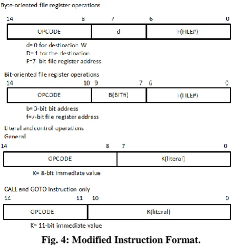
V. REVISED INSTRUCTION SET
[image:3.595.314.543.267.507.2]Integration of the CALU forces some changes in the original 8-bit RISC Core. Originally the RISC core has the instruction length of 14-bit. With the 14-bit instruction set, without affecting the original functionality of the instruction set there was no space for new instruction. So we needed to add one more bit to the instruction length. We have added this bit to the MSB side of the instruction op-code. For all the original instruction this MSB bit has been kept as '0' and for all the instruction which are added for the CALU operation this MSB bit is '1'. This bit distinguishes the old and new instructions. The change in the instruction length needed some other changes too. Like now for the new core, we need to have 15-bit wide program memory. The Addition of the 1 bit had affected the Instruction format. The modified instruction format is as shown in Fig. 4.
Fig. 4: Modified Instruction Format.
We have added 11 new instructions to the existing instruction set.
VI. RESULTS
The Implementation of 8-bit RISC core with the CALU is designed and developed in the Vivado 2017.3. The hardware platform selected for the functional verification is the Spartan 6 XC6SLX9-3TQG144.
A. Performance improvement:
The designed RISC core shows performance improvement in temporal domain for various cases. Assuming all operands are kept in data memory requires only 1 clock cycle.
Case I : 16-bit addition original core movf 30h,0;
[image:3.595.59.292.601.773.2]Fig. 5: 16-bit addition on original core 16-bit addition on enhanced core
addword; requires one clock cycle. Case II: 16-bit subtraction original core movf 30h,0;
[image:4.595.314.545.57.314.2]subwf 32h, 1; movf 33h,0; btfsc 03h,0; sublw 01h; addwf 31h,1;
Fig. 6: 16-bit subtraction on original core 16-bit subtraction on enhanced core
subword;
Case III: 16-bit AND operation original core movf 30h,0;
andwf 32h,1; movf 33h,0; andwf 31h,1;
Fig. 7: 16-bit AND operation on original core
16-bit AND operation on enhanced core andword;
Case IV: 16-bit OR operation original core movf 30h,0;
iorwf 32h,1; movf 33h,0; iorwf 31h,1;
Fig. 8: 16-bit OR operation on original core 16-bit OR operation on enhanced core
orword;
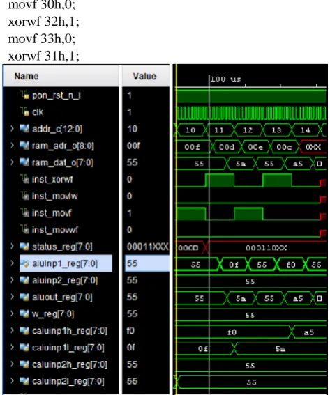
Case V: 16-bit XOR operation original core movf 30h,0;
xorwf 32h,1; movf 33h,0; xorwf 31h,1;
Fig. 9: 16-bit XOR operation on original core 16-bit XOR operation on enhanced core
xorword;
Case VI: 16-bit SWAP operation original core movf 04h,0;
[image:4.595.311.548.360.644.2] [image:4.595.61.296.508.772.2]International Journal of Innovative Technology and Exploring Engineering (IJITEE) ISSN: 2278-3075, Volume-8 Issue-9, July 2019
16-bit XOR operation on enhanced core swapword;
Case VII: 16-bit Increment operation original core movf 04h,0;
addlw 01h,0; movf 06h,0; btfsc 03h,0; addlw 01h;
16-bit Increment operation on enhanced core incword;
Case VIII: 16-bit Decrement operation original core movf 04h,0;
sublw 01h,0; movf 06h,0; btfsc 03h,0; sublw 01h;
16-bit Decrement operation on enhanced core Decword;
Case IX: 16-bit Right Shift operation original core rrf 06h,1;
rrf 04,1;
16-bit Right Shift operation on enhanced core rrword;
Case X: 16-bit Left Shift operation original core rlf 06h,1;
rlf 04,1;
[image:5.595.310.545.48.242.2]16-bit Left Shift operation on enhanced core rrword;
Fig.10: Execution of CALU instructions
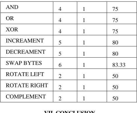
Fig. 10 shows 16-bit operations executed in Enhanced core with instructions of CALU. It can be observed that all the operations which needed 2 to 6 instructions have been completed in the single instruction, leading to the clock cycle saving. Percentage clock cycle saving is shown in the table below.
II) Percentage Clock Cycle Savings
16-BIT CYCLES
REQUIRED
% CYCLE
OPERATION
ON OLD PIC
ON MODIFI ED PIC
SAVING
ADDITION 6 1 83.33
SUBTRACTION 6 1 83.33
AND 4 1 75
OR 4 1 75
XOR 4 1 75
INCREAMENT 5 1 80
DECREAMENT 5 1 80
SWAP BYTES 6 1 83.33
ROTATE LEFT 2 1 50
ROTATE RIGHT 2 1 50
COMPLEMENT 2 1 50
VII. CONCLUSION
In the era of Internet of Things, It is needed to collect and process the data on the sensor nodes. For applications like sensor node processing industries demand low power consumption chips with maximum data handling and processing capabilities. In such an application our Enhanced 8-bit RISC can provide a solution. It consumes 15mW power. The core is powered by the Cooperative Arithmetic and Logical Unit, which has enhanced the data processing capabilities of the core.
The Implementation of 8-bit RISC core with CALU is designed and developed in the Vivado 2017.3. The hardware platform selected for the functional verification is the Spartan 6 XC6SLX9-3TQG144. The maximum clock frequency achieved on the selected device is 34.99MHz. The performance improvement has been recorded in terms of the clock cycles savings. Average performance improvement is 71% in multi-byte operational cases.
REFERENCES
1. R. P. Singh, A. K. Vashishtha, R. Krishna, "32 Bit re-configurable RISC Processor Design and Implementation for BETA ISA with inbuilt Matrix Multiplier," 2016 Sixth International Symposium on Embedded Computing and System Design (ISED), Patna, (2016), pp. 112-116.
2. R. Sharma, V. K. Sehgal, N. Nitin, P. Bhasker and I. Verma, "Design and Implementation of a 64-bit RISC processor using VHDL," 2009, 11th International Conference on Computer Modelling and Simulation, Cambridge, (2009), pp. 568-573.
3. Y. Ando, R. Sato, M. Tanaka, K. Takagi, N. Takagi, A. Fujimaki, "Design and Demonstration of an 8-bit bit-serial RSFQ microprocessor: CORE e4," in IEEE Transactions on Applied Superconductivity, vol. 26, no. 5, Aug.( 2016), pp. 1-5.
4. H. Woehrle, F. Kirchner, " CAEMO - A Flexible and Scalable High Performance Matrix Algebra coprocessor for Embedded Reconfigurable Computing Systems, in the journal “Microprocessors and Microsystems, vol. 56, Feb. (2018), pp. 47-63.
5. G. Jeong, J. Park, H. Jo, B. Yoon, M. Lee, "ARM7 compatible 32-bit RISC processor design and verification," Proceedings. The 9th Russian-Korean International Symposium on Science and Technology, 2005. KORUS 2005., Novosibirsk, Russia, (2005), pp. 607-610.
7. X. Liu, "An ultralow-voltage sensor node processor with diverse hardware acceleration and cognitive sampling for intelligent sensing," in IEEE Transactions on Circuits and Systems II: Express Briefs, vol. 62, no. 12, Dec. (2015), pp. 1149-1153.
8. J. Jeemon, "Low power pipelined 8-bit RISC processor design and implementation on FPGA," 2015 International Conference on Control, Instrumentation, Communication and Computational Technologies (ICCICCT), Kumaracoil, (2015), pp. 476-481. 9. Y. Ying, Z. Lei, M. Hao, "Design and VLSI Implementation of an
Asynchronous Low Power Microcontroller," ASICON 2001. 2001 4th International Conference on ASIC Proceedings (Cat. No.01TH8549), Shanghai, China, (2001), pp. 797-799.
10. A. Gupta, U. Malviya, V. Kapse, "Design of speed, energy and power efficient reversible logic based vedic ALU for digital processors," 2012 Nirma University International Conference on Engineering (NUiCONE), Ahmedabad, (2012), pp. 1-6.
11. P. Trivedi, R. P. Tripathi, "Design and analysis of 16 bit RISC processor using low power pipelining," International Conference on Computing, Communication and Automation, Noida, 2015, pp. 1294-1297.
12. J. Chiu, K. Yang, Y. Chou, "A Hyperscalar dual-core Architecture for Embedded Systems," in the journal “Microprocessors and Microsystems vol. 37, Issue 8, Part B, Nov. (2013), pp. 929-940 13. G. A. Malazgirt, A. Yurdakul , S. Niar," Customizing VLIW
Processors from Dynamically Profiled Execution Traces, " in the journal Microprocessors and Microsystems, vol. 39, Issue 8, Nov. (2015), pp. 656-673.
AUTHORS PROFILE
First Author Tanaji M.Dudhane received B.E.in Electronics Engineering in the year 1994 from Mumbai University and Pursued M.E. in VLSI & Embedded System from Savitribai Phule University of Pune, Maharashtra, India in the year 2011. Now Pursuing Ph.D. from Satyabama Institute of Science and Technology, Chennai, India.