Theses Thesis/Dissertation Collections
8-2013
Power Profile Obfuscation using RRAMs to
Counter DPA Attacks
Ganesh Chandrakantrao Khedkar
Follow this and additional works at:http://scholarworks.rit.edu/theses
This Thesis is brought to you for free and open access by the Thesis/Dissertation Collections at RIT Scholar Works. It has been accepted for inclusion in Theses by an authorized administrator of RIT Scholar Works. For more information, please [email protected].
Recommended Citation
Counter DPA Attacks
by
Ganesh Chandrakantrao Khedkar
A Thesis Submitted in Partial Fulfillment of the Requirements for the Degree of Master of Science in Computer Engineering
Supervised by
Dr. Dhireesha Kudithipudi Department of Computer Engineering
Kate Gleason College of Engineering Rochester Institute of Technology
Rochester, New York August 2013
Approved by:
Dr. Dhireesha Kudithipudi, Associate Professor Thesis Advisor, Department of Computer Engineering
Dr. Marcin Łukowiak, Associate Professor
Thesis Co-Advisor, Department of Computer Engineering
Dr. Amlan Ganguly, Assistant Professor
Rochester Institute of Technology Kate Gleason College of Engineering
Title:
Power Profile Obfuscation using RRAMs to Counter DPA Attacks
I, Ganesh Chandrakantrao Khedkar, hereby grant permission to the Wallace Memorial
Library to reproduce my thesis in whole or part.
Ganesh Chandrakantrao Khedkar
Dedication
Acknowledgments
I would like to express my deepest appreciation to all countless faculty, staff and friends,
who provided me the possibility to complete this work. A special gratitude I give to my
thesis advisor, Dr. Dhireesha Kudithipudi for her continual guidance, suggestion and help
to coordinate this work. I would like to thank Dr. Marcin Łukowiak for his precious
assistance improving my understanding of Side Channle Attacks and also for serving as a
committee member. I would also like to thank Dr. Amlan Ganguly for taking time out of
his busy schedule to serve as a committee member.
Furthermore I would also like to acknowledge with much appreciation the crucial role of
the Mr. Emilio Del Plato and Mr. Richard Tolleson who gave the permission to use all
required servers to complete the lengthy simulation tasks. A special thanks goes to Xuan
Tran, who helped me for the part of DPA attack. Last but not least, many thanks goes to
Cory Merkel, Sundarraman Mohanram, Sam Skalicky, and Gorden Werner for time to
Abstract
Side channel attacks, such as Differential Power Analysis (DPA), denote a special class of
attacks in which sensitive key information is unveiled through information extracted from
the physical device executing a cryptographic algorithm. This information leakage, known
as side channel information, occurs from computations in a non-ideal system composed of
electronic devices such as transistors. Power dissipation is one classic side channel source,
which relays information of the data being processed. DPA uses statistical analysis to
identify data-dependent correlations in sets of power measurements.
Countermeasures against DPA focus on hiding or masking techniques at different levels
of design abstraction and are typically associated with high power and area cost. Emerging
technologies such as Resistive Random Access Memory (RRAM), offer unique
opportuni-ties to mitigate DPAs with their inherent memristor device characteristics such as variability
in write time, ultra low power (0.1-3 pJ/bit), and high density (4F2).
In this research, an RRAM based architecture is proposed to mitigate the DPA attacks
by obfuscating the power profile. Specifically, a dual RRAM based memory module masks
the power dissipation of the actual transaction by accessing both the data and its
comple-ment from the memory in tandem. DPA attack resiliency for a 128-bit AES cryptoprocessor
using RRAM and CMOS memory modules is compared against baseline CMOS only
tech-nology. In the proposed AES architecture, four single port RRAM memory units store the
intermediate state of the encryption. The correlation between the state data and sets of
power measurement is masked due to power dissipated from inverse data access on dual
RRAM memory. A customized simulation framework is developed to design the attack
scenarios using Synopsys and Cadence tool suites, along with a Hamming weight DPA
attack module. The attack mounted on a baseline CMOS architecture is successful and the
AES cryptoprocessor yielded unsuccessful results with no keys recovered, demonstrating
Contents
Dedication. . . iii
Acknowledgments . . . iv
Abstract . . . v
1 Introduction and Background . . . 1
1.1 Resistive Random Access Memory . . . 1
1.2 Advanced Encryption Standard Algorithm . . . 4
1.2.1 SubBytes . . . 5
1.2.2 ShiftRows . . . 6
1.2.3 MixColumn . . . 6
1.2.4 AddRoundKey . . . 7
1.3 Side Channel Attacks . . . 7
1.4 Power Analysis Attack . . . 8
1.4.1 Simple Power Analysis . . . 10
1.4.2 Differential Power Analysis . . . 10
1.5 Contributions . . . 12
2 Related Work and Contributions . . . 14
2.1 DPA vulnerability in AES algorithm . . . 15
2.2 DPA mitigations techniques . . . 16
2.2.1 Masking . . . 16
2.2.2 Hiding . . . 17
2.3 Summary . . . 18
3 Hardware Architecture . . . 20
3.1 RRAM . . . 20
3.1.1 RRAM and other memory technologies . . . 20
3.1.2 RRAM Architecture . . . 21
3.2.1 AES Encryption Unit . . . 25
3.2.2 Memory Balancing Logic . . . 27
4 Simulation and Attack Framework . . . 31
4.1 Simulation Framework . . . 31
4.1.1 Power extraction for CMOS implementation . . . 32
4.1.2 RRAM power extraction . . . 34
4.2 Attack Framework . . . 35
4.3 Summary . . . 37
5 Result and Analysis . . . 38
5.1 Memristor . . . 38
5.2 RRAM power dissipation . . . 40
5.3 Balance Logic and Inverse State Memory . . . 43
5.4 DPA Attack Results . . . 46
5.5 Summary . . . 50
6 Conclusions and Future Work . . . 51
6.1 Conclusions . . . 51
6.2 Future Work . . . 52
List of Tables
2.1 Comparison chart depicting the cost incurred due to implementation of
each countermeasure when compared with unprotected design. . . 19
3.1 Qualitative Comparison between RRAM and other emerging and
commer-cialized memory technologies . . . 21
List of Figures
1.1 High-level overview of RRAM block architecture.[48] . . . 3
1.2 Generic Representation for the AES Algorithm . . . 5
1.3 The ShiftRows Transformations . . . 6
1.4 Types of unintended information leakage from cryptographic function im-plementation . . . 8
1.5 Overview of the power analysis attack flow [32] . . . 9
1.6 SPA Trace of entire DES algorithm [34] . . . 11
2.1 Basic overview of Masking approach [57] . . . 16
2.2 Architectural view of Multiprocessor balancing [6] . . . 18
3.1 Block level view of an NxM RRAM. . . 22
3.2 Power switching using a single power device . . . 24
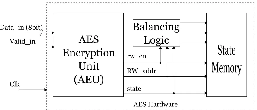
3.3 Top view of the proposed AES hardware design . . . 25
3.4 RTL representation of the AES Encryption Unit . . . 26
3.5 AES Control Unit State Machine . . . 26
3.6 RTL representation of the State Memory with Regular State Memory Bank and Inverse State Memory Bank . . . 29
3.7 RTL block diagram for the Balancing Logic with the snooper to engage both Regular Memory and Inverse Memory modules. . . 29
4.1 Top Level Simulation Flow for Power Extraction . . . 32
4.2 Synthesis flow to generate netlist and gate level simulation model . . . 33
4.3 Power modeling flow for AES Encryption Unit. . . 34
4.4 Power extraction flow for RRAM state memory model. . . 35
4.5 Top view of the attack module. . . 36
4.6 Differential Power Analysis overview for a single byte attack. . . 36
5.1 The I-V curve produced by linear memristor model. . . 39
5.2 The I-V curve produced by linear memristor model with temperature vari-ation. . . 39
5.4 Power dissipation when (a) Writing a one to the RRAM crossbar (b) Writ-ing a zero to the RRAM crossbar (c) ReadWrit-ing across the RRAM crossbar [32]. . . 41
5.5 Voltage variability analysis for the RRAM crsoosbar, when writing to 31st
bit in the first row. [32]. . . 42
5.6 Temperature variability analysis for the RRAM crsoosbar, when writing to
31st bit in the first row. [32]. . . 43
5.7 Waveform for read/write cycle on regular state memory and inverse state
memory. . . 43
5.8 Power dissipation for 1 round of AES for (a) Regular CMOS Memory (b)
Inverse CMOS State Memory (c) Total CMOS State Memory. . . 45
5.9 Power dissipation for 1 round of AES for (a) Regular RRAM Memory (b)
Inverse RRAM State Memory (c) Total RRAM State Memory . . . 46 5.10 Power comparison of Single/ Dual CMOS and RRAM memory
implemen-tation . . . 47
5.11 (a) Differential trace for AES with Regular CMOS state memory with 10, 000 power traces, all 16 key bytes (b)Confidence ratio for AES with
Regu-lar CMOS state memory with 10,000 power traces . . . 48
5.12 (a) Differential trace for AES with Regular RRAM state memory with 10, 000 power traces, all 16 key bytes (b)Confidence ratio for AES with
Regu-lar RRAM state memory with 10,000 power traces . . . 49
5.13 (a) Differential trace for AES with inverse CMOS state memory with 40, 000 power traces, all 16 key bytes (b)Confidence ratio for AES with inverse CMOS state memory with 40,000 power traces . . . 49 5.14 (a) Differential trace for AES with inverse RRAM state memory with 40,
Chapter 1
Introduction and Background
Modern security systems use cryptographic algorithms to provide confidentiality, integrity
and authentication of data. These cryptographic algorithms rely on mathematically
com-plex and difficult operations to enhance the security [61]. Research in cryptanalytic
tech-niques has demonstrated that secret information can be extracted by exploiting weaknesses
of a cryptographic algorithm’s implementation at hardware/software level [3]. As the
con-ventional hardware implementations are based on CMOS technology, efficacy of
counter-measures are confined by the technology limitations. These limitation include high static
and dynamic power dissipation. Several emerging technologies such as memristive devices
are being commercialized and adopted in the IC design market, it is equally important to
understand the effect of these devices on the overall system to improve resiliency against
cryptanalytic techniques.
1.1
Resistive Random Access Memory
The Resistive Random Access Memory (RRAM) is a crossbar resistive memory array, in
which the storage elements are two-terminal resistive switching element, known as
memris-tor. Memristor is a two terminal, passive circuit device that imposes a non-linear
relation-ship between electrical charge and magnetic flux linkage [13, 15]. From a behavioral point
of view, these devices are characterized by a pinched hysteresis current-voltage relationship
[14], indicating that their instantaneous resistance depends on the history of applied
Ron. The memristor’s resistance states can be read by applying a small non-destructive
voltage yielding a non-volatile memory behavior.
Unlike RRAM, many emerging non-volatile technologies such as Phase Change
Mem-ory (PCM), Spin-torque transfer random access memMem-ory (STTRAM), are being actively
researched [66, 78]. Compared to the conventional CMOS memories such as SRAM, these
emerging technologies are non-volatile, requiring a little/zero power to maintain the stored
state. Memristor based RRAM is a viable technology for future computing with high
den-sity, ultra-low static power consumption (limited by CMOS leakage power), low dynamic
power consumption (≈0.1-3 pJ/bit), high retention and endurance [77]. Semiconductor
companies such as HP, Toshiba are exploring the possibility of replacing SRAM on-chip
memory with the emerging memories like RRAM in the near future [75].
Memristor device modeling is a challenging task due to the diversity of physical
imple-mentations and proposed switching mechanisms [76, 77]. A common method, especially
in the case of transition metal oxide thin film implementations, is to treat the switching
region of the device as two variable resistors in series, where the total resistance is given
byRm =xRon+ (1−x)Rof f, wherexis a state variable that ranges from 0 to 1 [48, 69].
In the case of TiO2 switching regions,xis the fraction of the TiO2−x phase present in the
switching region. Analytically, this model can be described by
Rm(t) =Rm0 s
1−2η4Rφ(t)
D2R2 m0
µRon, (1.1)
where Rm0 is the maximum resistance (Rm0 ≈ Rof f), D is the film thickness,η (±1) is
the polarity of the applied voltage, Q0 the charge required for x to change from 0 to 1,
4R = Rof f −Ron, φ(t)is the time integral of the applied voltage, andµis the mobility
of defects or ion species. Based on equation (1.1) it is clear that the write time, or latency,
necessary to achieve target high and low resistance states will vary from device to device.
...
...
... ... ...
[image:15.612.180.440.86.367.2]...
Figure 1.1: High-level overview of RRAM block architecture.[48]
latency.
A generalized illustration of a CMOS/RRAM architecture is shown in Figure 1.1 [48].
The AnN×Mcrossbar array of thin-film memristors is used as the storage medium.
Cross-bar circuits offer high density and addressability [74]. The gray area represents
CMOS/-nano interface. All the components outside the gray box are implemented using CMOS,
everything inside the box is using nano-CMOS paradigms [47]. A single memristor from
the crossbar can be accessed via row and column multiplexers based on the address
pro-vided. A read/write control circuit is used to apply a read or (positive or negative) write
voltage depending upon value ofrw¯ . RRAM block is isolated using two tri-state buffer and
enable signal. Note that this is a bit-addressable block, so we combinebof these blocks in
1.2
Advanced Encryption Standard Algorithm
Advanced Encryption Standard (AES) algorithm is the standard for encryption, approved
by National Institute of Technology and Standard (NIST) in 2001 [1]. It is a symmetric
block cipher that processes 128-bit data blocks and can operate on keys with length of 128,
192, or 256 bits. The number of rounds depends on the key length.
The different transformations of the algorithm architecture operates on the intermediate
data blocks, knows as State. The State consists of 16 bytes arranged as a rectangular array
of four rows and four column. As a symmetric key encryption algorithm, the identical key
is used for the encryption and decryption of data. The equation (1.2) shows order followed
to access data during transformations.
State=
00 04 08 0C
01 05 09 0D
02 06 09 0E
03 07 0A 0F
(1.2)
There are several rounds of transformation, dictated by the key length. This number could
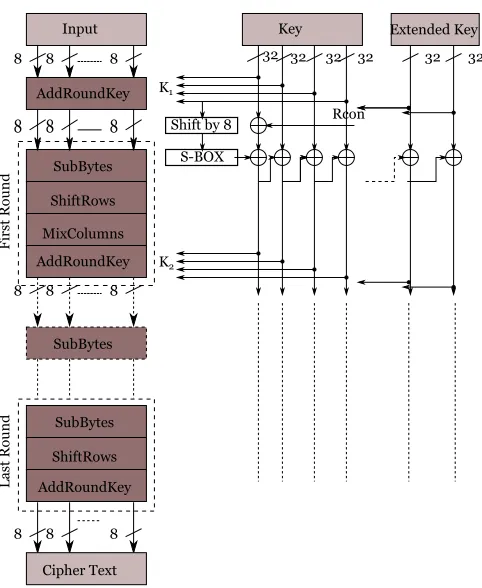
be 10, 12 and 14 for the key length of 128, 192 and 256 bit respectively. Figure 1.2 shows
the generic representation of the AES algorithm. Each round is consists at the max four
transformation, namely SubBytes, ShiftRows, MixColumns and AddRoundKey as shown
in Figure 1.2. The encryption cycle always begins with AddRoundKey transformation and
continues with internal rounds with all four transformations. The final round consists of
SubBytes, ShiftRows and AddRoundKey transformations only. Figure 1.2 also shows the
key expansion unit which generates the key for every round, from the primary key. When
all the rounds of transformation are performed, the cipher data of same block size as of
8 8 8
AddRoundKey
SubBytes
MixColumns ShiftRows
Input
SubBytes
ShiftRows
FirstTRoun
d
8 8 8
AddRoundKey
LastTRound
8 8 8
CipherTText
Key
K1
AddRoundKey
SubBytes
ShiftTbyT8 S-BOX
K2
Rcon 32 32 32 32
8 8 8
[image:17.612.190.431.89.383.2]ExtendedTKey 32 32
Figure 1.2: Generic Representation for the AES Algorithm
1.2.1 SubBytes
The SubByte transformation is the only nonlinear transformation within AES algorithm.
The byte substitution operates independently on each byte of the state using a substitution
box (S-box). This table is constructed using two transformations: multiplicative inverse
and affine transformation. First, the multiplicative inverse in the finite field of GF (28)
is taken, and then an affine transformation over GF(2) is applied. The SubByte can be
implemented as simple as Lookup Table (LUT) or can be calculated dynamically during
the transformation. The affine transformation for the encryption process is defined as
`
whereSi is theith bit of input byte and C(i)is the ith bit of the byte constant C with the
valueC = [01100011], as specified in the algorithm [1].
1.2.2 ShiftRows
The rows of the state are cyclically shifted over different offsets. This is done according to
the equation (1.4) [10], as shown in below
Sr,c =Sr,(c+shif t(r,N))modN (1.4)
As a result, the first row is unchanged, while the second, third and fourth row are cyclically
shifted to the left by one, two and three respectively as shown in Figure 1.3. This
transfor-a00 a10 a20 a30 a01 a11 a21 a31 a00 a10 a20 a30 a00 a10 a20 a30 a03 a13 a23 a33
a00 a01
a11 a21 a31 a00 a10 a20 a30 a00 a10 a03 a13 a23 a33 a02 a12 a22 a32
Figure 1.3: The ShiftRows Transformations
mation adds the diffusion property to each round transformation to confuse the relationship
between the plaintext input and ciphertext output.
1.2.3 MixColumn
The MixColumn transforms maps each of the input state to a new column in the output
state. Each input column is considered as a polynomial over GF(28) and multiplied with
p(x) = 03x3+ 01x2+ 01x+ 02mod(x4+ 1) (1.5a)
`
S(x) = p(x)⊕s(x) (1.5b)
1.2.4 AddRoundKey
At the end of every round, a round key is added to the data using a simple bitwise XOR
operation. The actual key is used only at the beginning of the AES encryption before
Round 1. During internal rounds AddRoundKey transformation Round keys are derived
from the key schedule using the initial cipher key using Rijndael key expansion algorithm.
The equation (1.6) illustrates the each round’s subkey computation.
W[i] =
w[i−4]⊕w[i−1] ifi mod 46= 0
w[i−4]⊕SubByte(RotW ord(w[i−1]))⊕Rcon[i] ifi mod 4 = 0 (1.6)
Wherew[i]is the expanded key. TheRotW ord()is a simple cyclic permutation of a word
change[a0, a1, a2, a3]to[a1, a2, a3, a0]. TheRcon(i)is the exponentiation of 2 performed
in Rijndael’s finite field in polynomial form as shown below.
Rcon[i] =x(i−1) modx8+x4+x3+x+ 1 (1.7)
And SubByte will apply S-box value in SubByte transformation to each of key byte.
1.3
Side Channel Attacks
The cryptographic algorithms are usually strong against mathematical attacks. The only
way to unlock the secret key is to try all possible combinations. A cipher is said to be
secure if larger the number of required combinations such that a complete search becomes
impossible. For instance, RSA-2048 bits can be used at least till the year 2030 before the
Traditional cryptanalysis views a cryptographic algorithm as a black box operation that
transforms the plaintext into ciphertext using a secret key and could attempt to exploit
the algorithm by analyzing imperfections in its mathematical structure [58]. However,
the cryptographic algorithm has to be implemented on a physical device, which will leak
additional information related to internal operation through unintended inputs and
out-puts knows as side channels [34]. Figure 1.4 shows such unintended information leakage
sources in the form of power, timing, electromagnetic induction etc.
Cryptographic Function Tamper Resistance
Electromagnetic Induction Power
Consumption
Computational
Fault Execution Time
Plaintext Ciphertext
Secrete Information
Figure 1.4: Types of unintended information leakage from cryptographic function implementation
Side Channel Attacks (SCA) attempt to exploit these side channels in order to extract
secret information from a cryptographic function implementation [2]. Depending upon
the targeted side channel information, attacks can be based on power [34], timing [20],
electromagnetic radiations [59].
1.4
Power Analysis Attack
In 1999, Kocher showed that instantaneous power consumption of a cryptographic system
can be related to secret data within the system [34]. This kind of attack can be mounted in
These attacks have been implemented against hundreds of devices, including
implementa-tions in ASICs, FPGAs, and softwares [35, 43]. The target devices ranges from tiny
single-purpose chips to complex devices whoes power measurements are noisy and obfuscated by
unpredictable parallel operations.
The goal of power analysis is to identify a relationship between the changing internal
state of the cryptographic device with respect to instantaneous power consumption. A
prop-erly identified intermediate step related to sensitive information will improve the chances
of successful extraction [3]. For instance, in an AES implementation, output of the first
transformation in the first round is dependent only on a known plaintext input and the
se-cret key. As a result, if a relationship can be found between this intermediate state and
circuit’s power consumption, then it could be possible to extract the secret key.
Figure 1.5 shows the overview of the power analysis attack flow. A cryptographic
func-tion takes a plaintext and compute an intermediate cipher using a secret key. Generally,
a sensitive data will represent the data stored in intermediate registers after computation
phase. The associated computational leakage will be observed. This sensitive data will be
attempted to predict using different key guess in attack model. In order to correlate the
sensitive data with each power trace, a leakage model must be constructed to describe the
power consumption of the device. The Hamming Weight and Hamming Distance are some
of the most typically used models to describe the leakage of these circuit elements [24].
Plaintext
Compute Secret Key
Guess Key Predict Computational
Leakage Model
Computational Leakage
Secrete Estimation
Cryptographic Function Attack Model
The Hamming Weight model is the straightforward representation of a device’s power
consumption. It is based on the assumption that power consumption is proportional to
num-ber of bits switched on. Though, power consumption using this model is weakly described,
but it is useful when little knowledge about the underlying hardware is available [24]. On
the other hand, Hamming Distance assumes that, number of bit transition is proportional to
power consumption of the circuit [50].
1.4.1 Simple Power Analysis
Simple Power Analysis (SPA) is a basic power analysis technique which involves direct
interpretation of power consumption measurements collected during a cryptographic
oper-ation . Number of power traces are observed to identify apparent characteristics that may
be useful to reveal information about sensitive operations [34]. This apparent features are
SPA weakness caused by operations performed based on key bits. This visible variations
results mainly from differences in the power consumption of different operations. Thus,
SPA is more helpful in determining the overall structure of an algorithm, not specifically in
determining its key.
For instance, Kocheret.al.[34], completed SPA on the Data Encryption Standard (DES)
algorithm in order to determine when each round occurs. Figure 1.6 clearly shows all 16
rounds of the DES algorithm. As identification of individual rounds within an encryption
operation helps to focus on the samples more likely to correlate thereby improving chances
of success of the attack [22]. This makes SPA useful tool for more sophisticated attacks.
As, SPA is limited to visual inspection, it is susceptible to noise or measurement errors.
1.4.2 Differential Power Analysis
Differential Power Analysis (DPA) is significantly more powerful statistical analysis
Figure 1.6: SPA Trace of entire DES algorithm [34]
[35]. The main advantage of DPA over SPA attacks is that no knowledge of the
crypto-graphic system and circuit is necessary [34]. However, DPA requires many traces of the
algorithm to work properly, often requiring several thousand traces.
A DPA attack attempts to guess secret information by establishing a relationship
be-tween the secret information and the instantaneous power consumption of the device. To
achieve this, a state within the system that is dependent upon both the secret and some
known quantity is identified. This state is referred to as the sensitive value, and may be
estimated by guessing the secret value by applying some known input. If the sensitive
value is correlated to the circuit’s power consumption, then a correct guess of the secret
will correlated to the power consumption [34, 35].
For instance, to perform a DPA attack on a block cipher, a selection functionD(P, b, Ks)
is defined for the plaintext (or ciphertext) P, for target bits b of sensitive state with key
guess Ks. Then encryption operations observed will haven corresponding power traces
ofksamples each, labeled asT1..n[1..k], along with related plaintext (or ciphertext)P1..n.
The two average traces are computed,A0 andA1. The average traceA1 is computed as
teh average of the power traces for whichD(P, b, Ks)produces one, andA0 as the average
of the power traces for which D(P, b, Ks) produces zero. Then distance between these
∆D[j] = Pn
i=1D(Pi, b, Ks)Ti[j] Pn
i=1D(Pi, b, Ks) −
Pn
i=1(1−D(Pi, b, Ks))Ti[j] Pn
i=1(1−D(Pi, b, Ks)) ≈2(
Pn
i=1D(Pi, b, Ks)Ti[j] Pn
i=1D(Pi, b, Ks) −
Pn i=1Ti[j]
n )
(1.8)
For incorrect guess ofKs, the bit computed usingDwill differ from the actual target bit
for about half of the plaintextPi. Thus, making selection functionD(Pi, b, Ks)completely
uncorrelated from the actual computation. As the power traces are divided in to two subsets
A1 andA0 randomly, the difference between the two average traces should approach zero
as the number of power traces increases [34, 35] as shown below.
lim
n→∞∆D[j]≈0 (1.9)
However, computed value of D(Pi, b, Ks) will be equal to actual value of target bit b
with probability 1 if theKsis correct. As a result,∆D[j]will approach to the actual power
consumption asn→ ∞.
1.5
Contributions
The primary goal of this research is to explore possible role of emerging technologies
such as RRAM in improving resiliency against DPAs in order to develop secure hardware
designs. This work expands upon an existing attack methodology developed for power
analysis attacks on a simulated implementation of the AES block cipher [65]. In order to
accomplish this goal,
• The existing RRAM architecture [47] has been altered to make it compatible to
exist-ing AES CMOS implementation.
• AES design also been modified to support RRAM and in order to provide a fair and
• Two architecture with CMOS memory and RRAM are developed and studied in a
simulated environment using Synopsys and Cadence tools.
• A DPA attack module is implemented and resiliency with and without countermeasure
is been tested.
The rest of the document is organized as follows: the related work of this thesis are
discussed in Chapter 2. Chapter 3 discusses the proposed architecture in detail. Simulation
and attack framework is discussed in Chapter 4. The results are discussed and analyzed in
Chapter 2
Related Work and Contributions
Side channel attacks attempt to reveal the secure data through information extracted from
physical implementation of a cryptographic function [49]. The device leaks information
through unintentional environmental interactions in the form of power, timing,
electro-magnetic radiations. Such unintentional information leakage occurs because computations
occur on a non-ideal system, composed of electronic devices such as transistors, wires,
power supplies, memory, and peripherals. Each of these component have characteristics
that vary with the instructions and data being processed. When this variance (side channel
information) is measurable, it becomes access point to an otherwise secure system.
One such side channel information is the instantaneous power consumption of a system.
Power attacks such as DPAs use power traces to correlate with secure data processed by
a cryptographic algorithm implementation [34, 49]. Several successful attacks to extract
secure key from a cryptographic system includes memory encryption/decryption schemes
[17] and power consumption randomization [19]. Successful attacks on embedded
sys-tems such as Virtex-II FPGA [51], Virtex-4/5 FPGA [52] bitstream encryption, and Atmel
Cryptomemory non-volatile memory [9] proves that these attacks are practical and lethal.
Therefore, it is critical to evaluate countermeasures that hamper power attacks.
Counter-measures are mainly focused on achieving a disconnect between the secured data/operation
executed and its power consumption [55].
In this chapter, AES algorithms vulnerability towards DPA is discussed first. In
2.1
DPA vulnerability in AES algorithm
The encryption cycle of AES algorithm, as discussed in section 1.2, processes plaintext
using the round keys derived form cipher key in multiple rounds. At any point within
dat-apath where the state (derived from the plaintext) and the round key (derived from cipher
key) enter a logic gate, the dynamic power consumption of this gate depends on both the
cipher-key and plaintext. If this information sampled, DPA attack can be mounted
success-fully. In essence, the output of any transformation in AES could be considered for an attack
[57]. Thus, the DPA vulnerability of the intermediate results is greatly dependent on the
specific implementation of the datapath.
The ShiftRows function is a simple bit permutation, and is realized using only wiring
for 128-bit parallel datapaths and hence, is not suitable for DPA attacks. Any non-linear
function increases the efficiency of the statistical attacks such as a DPA [35, 49]. Thus, an
efficient attack would target the output of the SubBytes transformation.
The MixColumn transformation is also a non-linear operation and is defined for 32 bits.
Attacking this output will require key hypothesis of232. Thus, making it a costlier, in terms
of required time and memory, compared to alternatives AES transformations. Finally, the
AddRoundKey transformation involves round key XORed with intermediate state. This
function is directly related to round key, but it is less efficient to attack than SubByte as
operation is linear.
A successful DPA attack on the AES implementation is presented in [44, 54]. Both
designs use 128-bit data path and one entire round transformation is performed in a single
cycle. Design attacked in [54], is a unprotected implementation of the AES. This attack
required 64,000 measurements for a successful extraction of the entire AES key. On the
other hand, design in [44] is protected implementation of AES using masking and required
2.2
DPA mitigations techniques
DPA Countermeasures attempts to obscure the relationship between the power profile and
the data/operation executed. To mitigate DPA, there are two broad categories of
counter-measures: masking and hiding. In this thesis, we base our solution on hiding.
2.2.1 Masking
Masking obscures the actual computation information by either adding or multiplying
ran-dom number’s to algorithm’s input and intermediate output values, making it difficult
to build correlation between power consumption and different cryptographic operations
[18]. This involves concealing every intermediate valuev by a random maskmsuch that
vm = v ∗m [43] as shown in Figure 2.1. In this way all the intermediate data appears to
be nonaligned within the cryptographic system. There are mainly two types of masking :
boolean and arithmetic [18]. Boolean masks work by exclusive-oring the data value with
the mask given asvm =v⊕m. Arithmetic masks work by either adding or multiplying the
mask to the data using modular addition or multiplication.
Masking Plaintext
Masking Algorithm
Modified -Encryption Algorithm
Un-masking
Ciphertext
Figure 2.1: Basic overview of Masking approach [57]
Once mask is inserted into the intermediate values, it must be eventually removed as
shown in Figure 2.1. Masking the S-Box is a difficult task. This difficulty is associated
with non-linearity [67]. Different method have been proposed to achieve masking of
S-BOX in [63, 67]. However, implementation of these measures is highly algorithm-specific
the intermediate data and the power consumption, but are not most effective against higher
order DPA [63].
2.2.2 Hiding
The goal of hiding technique is to level the system’s temporal power profile. In other
words, these techniques cause the instantaneous power consumption to be approximately
constant, regardless of the cryptographic operation being performed [17, 56, 64]. This
can be achieved either by randomizing the power consumption over a given period [28]
or by flattening the power consumption so that the power used by device is equal over all
operations [53]. Some of the techniques used are randomization [28, 39, 45], dual rail logic
[25, 56, 62, 72], current flattening[8, 36, 53], bit-balancing [6, 7].
The main intent behind the randomization is to prevent power trace alignment,
there-fore thwarting the DPA. This can be achieved by either inserting random access pattern
[45] or randomizing the execution pattern of the algorithm [28]. As in [45], random
reg-ister renaming is used to disassociate the power consumption from its re-accessing. This
methodology requires a random number generator and a bigger register file to improve the
probability of the desired randomness. In case of [28], instructions are randomly executed
in run time to generate random power profile. Both techniques are highly algorithm
de-pendent and require pseudo-randomness. An efficient pseudo-random number generator
should have minimal effect on the size and speed of the circuit.
One of the well-known hiding countermeasure is to flatten the power signature of all
components, within the circuit’s hardware, independent of data value. An effective method
is performed at the cell level using Dual-Rail Precharge (DRP) logic blocks [56]. The
concept behind the DRP logic is to create logic cells that make power consumption constant
during each clock cycle. Every input and output into cell is paired with its inverse and
therefore a constant balance of ’0’s and ’1’s is maintained at any given point of time [25,
power dissipation logic for any bit transition. Though leveling power profile proves to be
effective, it will double the size of the circuit, increase the power required by 2-3X [6, 28],
and finally slows the circuit down by at least 50% due to additional stages [55].
Similar to flattening, bit-balancing attempts to balance bit-flips for every intermediate
value. This balancing is achieved by executing similar algorithm processing inverted data
in tandem [7] as shown in Figure 2.2. The Hamming Weight for all the intermediate
val-ues will be equal when normal and inverted data execution is considered. Although, the
architecture should be combined such that footprints related to execution in separate cores
cannot be inferred [6]. It is evident that bit-balancing doubles the area and power used
Normal Processor
Balancing Processor
Application Complement
Application
Figure 2.2: Architectural view of Multiprocessor balancing [6]
by the circuit. However, the overhead circuitry doesn’t change the speed of the algorithm
distinctly [6, 7].
2.3
Summary
Two main DPA countermeasures that are effective for AES are hiding and masking. Hiding
attempts to camouflage the key message with random (or additive) noise generated from
the underlying circuit/logic or use other means such as timing variance to disassociate the
information and the power signal [23]. Masking hides the actual computation information
[18]. Each of these countermeasures can be applied at multiple levels of integration -
algo-rithm level, logic level, and/or circuit level. Countermeasures such as WDDL [72], current
flattening [53], and multiplicative masking [73], have been adopted at different integration
levels, albeit at a high cost in performance, power consumption, and area. Table 2.1
com-pares cost in design parameters introduced by implementing a few of such countermeasures
Masking Randomization Dual Rail Logic Bit Flip
Type Logic Level Architectural/Algorithm Level Circuit/Logic Level Architectural level
Area 1.6X <1.3X 2X 2X
Time 1.3X - 1.4X 1.2X - 1.5X 1.5X - 1.7X 1.1X
Power 1.4X-1.6X 1.15X-1.3X 2X-3X 2X
Traces 20,000 [21] 30,000 [] 35,000 [] 40,000 []
Table 2.1: Comparison chart depicting the cost incurred due to implementation of each countermeasure when compared with unprotected design.
Few of these countermeasures can be applied to only private-key crypto systems and
few of them are suitable for public-key crypto systems. Furthermore, all of these
counter-measures have been explored as conventional CMOS implementations.
These countermeasures are highly algorithm dependent and require significant design
time effort. The effectiveness of any countermeasure is measured by the number of power
traces needed to extract a key. The goal is then to create a countermeasure that is a)
al-gorithm independent, b) consumes less power, c) has less effect on execution time, and d)
requires minimum design time efforts.
Since several emerging technologies such as memristive devices are being
commercial-ized and adopted in the IC design market, it is equally important to understand the effect of
Chapter 3
Hardware Architecture
An AES core module with S-BOX implementation has been used for power analysis attack
in this work. At abstract level, the design consists of AES transformation modules along
with RRAM based state memory.
This chapter starts with discussing the RRAM and its internal architectural details. In
subsequent section, the AES design has been discussed with proposed method to counter
the DPA.
3.1
RRAM
In this section characteristics of RRAM are compared with other emerging and commercial
memory technologies. In addition, the architecture of the RRAM used in this work is also
discussed.
3.1.1 RRAM and other memory technologies
Continued technology migration in to nanometer domain, has initiated research in several
hybrid CMOS/nano logic and memory architectures, each of these technology targets high
density and low power consumption with little or no performance degradation [16]. The
discovery of memristance in nanoscale metal-oxide devices [13, 68] has boosted the work
in nanoscale architectures to implement nonconventional logic to improve memory and
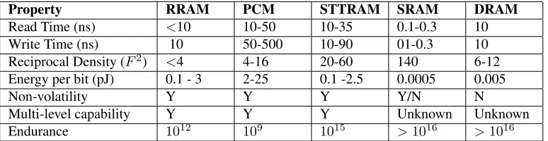
logic density [30]. Table 3.1 [42, 77] shows a qualitative comparison between RRAM and
Property RRAM PCM STTRAM SRAM DRAM
Read Time (ns) <10 10-50 10-35 0.1-0.3 10
Write Time (ns) 10 50-500 10-90 01-0.3 10
Reciprocal Density (F2) <4 4-16 20-60 140 6-12
Energy per bit (pJ) 0.1 - 3 2-25 0.1 -2.5 0.0005 0.005
Non-volatility Y Y Y Y/N N
Multi-level capability Y Y Y Unknown Unknown
[image:33.612.118.505.89.189.2]Endurance 1012 109 1015 >1016 >1016
Table 3.1: Qualitative Comparison between RRAM and other emerging and commercialized memory tech-nologies
due to smaller cell size. In addition, RRAM offers low operating voltages and multi-level
cell storage. A 40 nm 3-bit/cell and 2-bit/cell RRAM operation was demonstrated in [12].
The RRAM has very good write and read speed compare to other emerging technology but
lower than conventional SRAMs. Although RRAM has high leakage power as compare to
PCM and STTRAM, dynamic power consumption is very low. RRAM can withstand the
temperature up to 200◦ C [38]. However, RRAM has the problem of limited endurance.
RRAM suffers from the problem known as sneak path [40]. Previous work on resistive
memories with bidirectional resistive switches employed diodes and transistors to
elim-inate sneak paths reduce leakage current [26, 27, 37]. More sophisticated circuit level
techniques has been proposed to further suppression of sneak path in [42, 31]. Despite the
above challenges, the advantages such as low static power, low dynamic power compared
to conventional CMOS memories makes a power efficient replacement in this work.
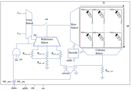
3.1.2 RRAM Architecture
A RRAM is the bit-addressable memory as shown in Figure 3.1 and is based on [47] .
CMOS/memristor RRAM architecture combines memristor crossbar circuits with
addi-tional CMOS circuitry to yield high-density non-volatile RRAM. Figure 3.1 depicts
gen-eralize CMOS/memristor hybrid RRAM architecture. In the top-right corner, an NxM
crossbar array is used as the physical storage medium. Each memristor stores a single bit
back-end CMOS process. The purple color square around the crossbar array represents the
CMOS/nano interface. Multiplexers are used to select data from a specific row or column
depending on the address given. A single memristor is isolated from the crossbar with the
Row Select
Column Select Decode
addr vrow
Select
Rref_wo Rref_w1 Rref_rd
Rpd_ref
vcoms
Rpd_col Reference
Select
vwr
vrd
rw
en rw
rw_en rw_en
data addr rw en en
N
[image:34.612.100.520.161.455.2]M
Figure 3.1: Block level view of an NxM RRAM.
help of address decoder. A read/write control circuit applies a read or write voltage
de-pending on the value ofrw¯ . Two tristate buffers and an enable signal are used to isolate the
RRAM block when it is not being used.
Read Operation
In the read operation,enshould be high andrw¯ should be low. This selects the read voltage,
vr, to be applied to the positive terminal of the memristor at the row and column specified
by the address. The read voltage is small enough such that it doen’t disturb the state of
voltage. The reference voltage is given by the voltage division
vref =vrow ×
Rpd col
Rref i+Rpd col
(3.1)
where vrow is the voltage applied to the selected crossbar row, andRref i is either Rref r,
Rref w0, orRref w1, depending upon operation.
Write Operation
Write operation is the most power consuming operation. The rate of change in the
mem-ristance depends on the voltage applied, and time [68]. There are two regions of operation
in case of memristor, linear and nonlinear. The linear mode of operation yields very low
energy metrics with a larger write time penalty while the nonlinear mode provides for much
faster speed but with higher power consumption [42]. In this work, the linear mode of the
operation is used as it is necessary to have low power dissipation and minimum difference
of power dissipation as compare to read operation.
The base design proposed in [47], requires two different voltage sources depending on
the data to be written. A positive voltage is required if the data signal is high, which forces
the memristor in low resistance state. A negative write voltage ensures a high resistance
state, when data signal is low.
To support multiple voltages in CMOS circuitry a DC-DC converter is required [11].
The current architectural optimization in CMOS technology has enabled supply voltage in
the order of 1V. This constrains the DC-DC circuitry to be highly efficient, low voltage and
low-current [11, 29].
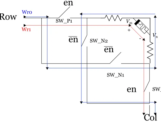
In this research, a simple approach has been used to eliminate the requirement of two
different power supply. Four control switches has been connected as shown in Figure 3.2.
Any two switches will be closed during each operation. To write ’1’ in the memristor, a
positive voltage needs to be applied at Vm with respect toVn. To ensure this SW P1 and
en
en
en
en
Row
Col
Wr1
Wr0
SW_P1
SW_P2 SW_N2
SW_N1 Vm
+
[image:36.612.177.449.100.309.2]- Vn
Figure 3.2: Power switching using a single power device
terminal (−), as shown by red line. If data to be written is ’0’, then a negative voltage
needs to be applied atVm with respect to Vn. Thus, effectively enabling current in reverse
direction. This is achieved by enabling SW N1 and SW N2 during data ’0’ writing, and
current direction is depicted by blue line in Figure 3.2.
3.2
AES architecture
The AES implementation used in this research is based on [65], designed to encrypt with a
128-bit cipher key. This design is constructed in a structural manner. Figure 3.3 depicts the
top view of the AES implementation under consideration. It consists of two main blocks,
1) AES Encryption Unit (AEU) and 2) Memory Balancing Logic.
The AES encryption unit performs transformation at byte level which uses the state
memory to store the intermediate state. The balancing logic block generates balancing
rw_en
RW_addr
state
AESg
Encryptiong
Unit
(AEU)
Data_ing(8bit)
Valid_in
Clk
Balancingg
Logic
Stateg
Memory
[image:37.612.100.530.91.275.2]AESgHardware
Figure 3.3: Top view of the proposed AES hardware design
3.2.1 AES Encryption Unit
This is a single entity which acts as a execution and control unit for the AES design. The
encryption unit has all the execution units for the four transformations of AES:
AddRound-Key, SubByte, ShiftRows, and MixColumns.
Figure 3.4 illustrates the RTL representation of the AES Encryption Unit. The
execu-tion units for the four transformaexecu-tions of AES are lined up and grouped together along
with a control unit. The SubByte unit performs the non-linear inversion in the Galois Field
GF(28). This is implemented as a look-up table. The ShiftRows transformation is
imple-mented as direct connection, as it changes only the location and not the byte values of the
state values during transformation. The control unit reorders the byte during this step of
the encryption. The bytes are simply read from a location and then written to a different
row address in the State memory.
The MixColumns requires access to a byte in all four rows simultaneously. This is
the driving factor behind having separate memory blocks for each row in the state matrix.
AddRoundKey is a simple XOR operation between an input byte of the state and a byte
W SubBytes ShiftRows MixColumns AddRoundKey KeyWMemory Block Decoder Key_addr RD_ROW WR_ROW DATA_IN OP_SEL RW_addr AESWControl WUnit RW_ADDR RW_EN STATE
Figure 3.4: RTL representation of the AES Encryption Unit
Memory Block.
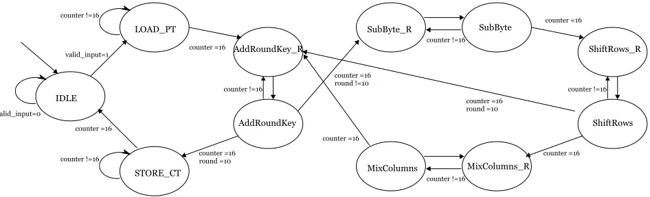
The AEU module also has a simple state machine to drive the datapath using AES
con-trol unit. This concon-trol state machine is shown in Figure 3.5. The concon-trol unit orchestrates
the datapath blocks to process one byte of the state matrix every two cycles. One cycle
to fetch the data from state memory and second to process the data. Therefore, each AES
transformation requires 32 clock cycles.
IDLE valid_input=0 LOAD_PT counterKy=16 valid_input=1 STORE_CT counterKy=16 counterK=16 AddRoundKey_R AddRoundKey counterK=16 counterK=16 counterKy=16 roundK=10 SubByte_R counterK=16 roundKy=10 SubByte counterKy=16 ShiftRows_R ShiftRows counterKy=16 counterK=16 MixColumns MixColumns_R counterKy=16 counterK=16 counterK=16 roundK=10 counterK=16
Figure 3.5: AES Control Unit State Machine
[image:38.612.100.573.501.645.2]This is followed by initial operation AddRoundKey. For every other clock cycle, each byte
will be fetched during AddRoundKey R state and XORed with cipher key in
AddRound-Key state. Since the operation is independent between bytes in the state, the output byte
is stored by replacing the input byte. SubByte operation is also performed in same
fash-ion. The ShiftRows operation changes the location of the state data of each row of state
matrix. This is achieved by relocating bytes from one bank to another bank. During the
MixColumns transformation, the four bytes of each column of the state matrix are
com-bined using an invertible linear transformation. This single step will be performed over 8
clock cycles. During which each input byte will affect all four output bytes. Hence, the
output bytes are stored in different memory bank in the state memory.
MixColumns transformation is not performed during final round of encryption cycle.
So, control is transfered from ShiftRows to AddRoundKey. Finally, the ciphertext is
re-trieved and stored one byte at a time, requiring an additional 16 cycles. The total encryption
requires 1344 clock cycles, as summarized in equation 3.2, wheretranf cyclerepresents
the number of transformation multiplied by clock cycles per transformation.
T otal cycles =Load P T+AddRoundKey+rounds×transf cycle+Store CT (3.2)
T otal cycles= 16 + 32 + 10×(4×32) + 16 (3.3)
T otal cycles = 1344 (3.4)
3.2.2 Memory Balancing Logic
Memory balancing logic consists of state memory, dual state memory and balancing logic.
There are four identical memories in the state memory and the dual state memory, named
as row memory as shown in Fig. 3.6. Each memory unit stores a row of the state matrix.
The power consumption of the memory is dependent of the data being read or written. For
instance, power dissipation for writing data ’1’ is different than writing data ’0’. This
noticeable difference in power dissipation can server as a side channel information for
the power attacks. The power consumption adds up as multiple bit data accessed. For
example, in case of 8-bit data bus, power consumption while writing data B’1111 0000 will
be addition of power dissipation of four one’s and four zero’s when accessed separately.
Also it is found that, the power dissipation is additive if multiple memories are accessed
simultaneously. The maximum power dissipation occurs when the accessed eight bit data
is all ’1’. Thus, for a data access having less than eight 1, a another data with remaining
number of 1’s should be accessed to yield the total eight 1’s. This additional data can be
simultaneously accessed from another memory of equal size. This was the motivation for
introducing a dual equal size memory in tandem. However, the additional memory will
incur cost in terms of power and area. Hence, minimizing this extra cost was one of the
motivation for looking beyond the conventional CMOS memory.
Emerging technologies such as RRAM, has high density, and ultra low power [77]
mak-ing them viable next generation on-chip memory. Additionally, a few research groups
are exploring the applicability of RRAM technologies for hardware security enhancement
[32, 41, 60]. Thus, a logical choice for alternative memory technology was RRAM which
helps to minimize power and area overhead with improved security. Therefore, regular
memory and inverse memory are implemented using RRAM. When a row memory from
state memory is accessed, then associated row memory from inverse state memory will also
be accessed in tandem. The dual memory is interfaced to the AES control block using the
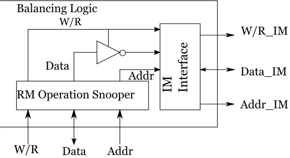
balancing logic block (BL).
The balancing logic block is a CMOS-based digital logic block. Fig. 3.7 depicts the
internal structure of the balancing logic block. The balancing logic block snoops the access
Row1 RRAM wr_rd wr_addr Data Row2 RRAM wr_rd wr_addr Data Row3 RRAM wr_rd wr_addr Data Row4 RRAM wr_rd wr_addr Data
Regular State Memory
wr_rd[4 bit] Addr Data Row1 RRAM wr_rd wr_addr Data Row2 RRAM wr_rd wr_addr Data Row3 RRAM wr_rd wr_addr Data Row4 RRAM wr_rd wr_addr Data
Inverse State Memory
Addr Data
[image:41.612.176.449.94.410.2]wr_rd[4 bit]
Figure 3.6: RTL representation of the State Memory with Regular State Memory Bank and Inverse State Memory Bank
and then generates correlated actions for inverse state memory. The snooping function
W/R Data Addr
W/R_IM Data_IM Addr_IM Balancing Logic Data Addr RM Operation Snooper IM Inte
rfac
e
W/R
[image:41.612.168.451.509.663.2]monitors the type of operation (read or write), address being accessed, and data. In the
case of a write operation a byte is written to the state memory while its complement is
written to the dual state memory. The goal is to consume power required for writing all
ones at any given point of time. For example, when the write operation on the regular state
memory is ”13”(H) then the data written on the dual state memory will be ”EC”(H). Thus,
Chapter 4
Simulation and Attack Framework
This chapter discusses the simulation framework to trigger a DPA attack on the proposed
architecture. To mount DPA attack, power traces are generated by simulating the execution
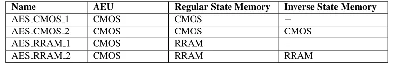
of hardware implementation. Four different architectures, as shown in Table 4.1, have been
simulated and attacked.
Name AEU Regular State Memory Inverse State Memory
AES CMOS 1 CMOS CMOS −
AES CMOS 2 CMOS CMOS CMOS
AES RRAM 1 CMOS RRAM −
[image:43.612.110.509.361.427.2]AES RRAM 2 CMOS RRAM RRAM
Table 4.1: AES design variations under consideration
In section 4.1, the simulation framework used in this work is discussed. Attack
frame-work is discussed in section 4.2.
4.1
Simulation Framework
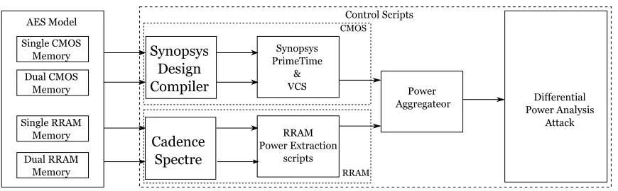
A customized flow is designed in this work due to the use of CMOS and RRAM modules in
the design. Figure 4.1 depicts the simulation power extraction flow for CMOS and RRAM
modules. Power extraction of CMOS involves two steps and is based on the work in [65].
First the hardware design is compiled and synthesized into an gate level implementation.
Then this gate level implementation is simulated several times with different plaintext
evaluation. This flow utilizes Synopsys tools for compilation, synthesis, and simulation of
the hardware design.
[image:44.612.99.534.143.278.2]AESfModel SinglefCMOSf Memory DualfCMOSf Memory SinglefRRAMf Memory Synopsysf Designf Compiler Synopsys PrimeTime & VCS RRAM PowerfExtraction scripts ControlfScripts Cadencef Spectre Differentialf PowerfAnalysisf Attackf DualfRRAMf Memory Power fAggregateor CMOS RRAM
Figure 4.1: Top Level Simulation Flow for Power Extraction .
In case of RRAM, power extraction involves simulation using Cadence tools. Power
information is extracted and stored along with input plaintext information. Several other
scripts are used for supporting the simulated power extraction. A plaintext input generator
(not shown in figure) is used to ensure that the similar plaintext is fed into CMOS and
RRAM simulation.
This research requires the collection of several thousands of power traces. The fact that,
each encryption cycle for a plaintext in independent of one another, opened the possibility
of dividing the number of encryption cycles over multiple cores to accelerate the power
extraction process. A top level Python based script has been created to control this feature
and entire flow.
4.1.1 Power extraction for CMOS implementation
Compilation and synthesis is one time overhead to generate the gate level simulation model.
The power extraction is automated using a Makefile which is invoked by top python script.
This ensures the dependency tracking for the intermediate resources. The arguments for
The modified hardware model of the AES used in this research is written in the
Sys-temVerilog. Figure 4.2 shows the entire flow for synthesis and simulation executable
gen-eration for CMOS implementation of AES. DC Shell reads the HDL along with technology
library (120nm) to generate the gate level simulation model and netlist.
SystemVerilog Source
technology_lib.db
DC Shell
aes_encryption_unit.vg *.syn
[image:45.612.156.468.189.317.2]synth_script
Figure 4.2: Synthesis flow to generate netlist and gate level simulation model .
For the purpose of extracting instantaneous power consumption for the AES Encryption
Unit, the activity data (VCD) in generated and fed to the power analysis engine directly as
shown in Figure 4.3. The piped simulation of the VCS tool with pt shell reduces the
over-head of performing a separate simulation. The SystemVerilog testbench reads the plaintext
inputs from the external file. The length of the plaintext file is specified by Verilog plusargs.
Testbench is also interfaced with state memory model written in SystemVerilog. This
en-sures the correctness of encryption without extracting the power for memory.
Each simulation generates two types of output files. A Nanosimout formatted
wave-form containing the power traces for each operation simulated (power waveform.out)
and a file containing plaintext and ciphertext along with start timestamp (simulation.txt).
Listing 4.1 shows one such example of simulation file. The trace loader requires the initial
Pt_Shellx
VCSx power_analysis.script
AES_encryption_unit.vg
constrain.sdc
testbench.sv
State_Memory_model.sv
power_waveform.out
simulation.txt plaintext.txt
[image:46.612.98.524.91.252.2]Make
Figure 4.3: Power modeling flow for AES Encryption Unit.
1 50 d54b6b3b4f95b25b328cb43566101a1f 6ceba27832d6ce7f742df828fe5e974c
2 21550 59e11bb21c78c469d6087640d827d51c 0a1777abff9f1f522552c49536a7d2f9
3 43050 de4f8f069101b56ca380a674ffa00181 465bd05353c8d6e308e536305cf1614b
4 64550 34f02c1c9a154dcb7a270964f7ac73c5 706838ca365c1b89ae841390f729c634
5 86050 bbcdb3228f3e2049868a39cbcff8608c 6614cef4179f401cee269e4362b42f1a
6 107550 2acbe0bf56a8744da769fd6c1fd2290c 3eee12b2bd16589f14b2f452c3f74204
7 129050 f94f15a15781bd384628aa995d305d62 a2fab777bc30464830cef5be640865b2
8 150550 0ab7395021af42cd86470e68b4273202 07755c83221deb57cca68b5f95bb1e15
9 ... ... ...
Listing 4.1: Simulation timestamp with plaintext and ciphertext
4.1.2 RRAM power extraction
The scond part of the extraction flow is for the RRAM section of the design. The
mem-ory system including row and column decoders and read/write circuitry is implemented
using 45nm CMOS transistors and gates (Berkeley PTM models). The memristor used
has following metrics Ron = 10KΩ, Rof f = 1MΩ, width = 40 nm, hight=60nm and is
been implemented in 60 nm technology [4, 5]. The entire RRAM system, circuits and
devices were modeled using Verilog-AMS language. This RRAM is interfaced with AES
encryption model implemented using Verilog. Thus, it is necessary to use a tool set with
a mixed signal simulation environment. Cadence Virtuoso AMS Designer tool compiles,
tool is a waveform database (.trn). A python based script is used to calculate the power
information and generate the power waveform similar to Nanosimoutfile format.
ncvlog ncelab ncsim
CadencefVirtuosofAMSfDesigner
RRAMfState Memory.fvams
testbench.v
AESfencryption model.v
controlfscript *.tcl
*.scs
waveformfdatabase *.ftrn
simulation.txt
Shellfscript
Power extractionfscript
power_waveformf *.fout
[image:47.612.98.577.136.329.2]pythonfscript plaintext.txt
Figure 4.4: Power extraction flow for RRAM state memory model.
Finally a power extracted from CMOS based AES encryption unit and RRAM is summed
up and stored inpower waveform.outformat, along with simulation timestamp file.
4.2
Attack Framework
The goal of the attacking framework is to achieve consistency in evaluating each of the
simulated designs for power analysis and secret key extraction. The attacking module
requires access to a number of instantaneous power consumption traces sampled over the
time during which the secret key was used to encrypt the given plaintext.
The main concern is maintaining data precision, in order to avoid losing valuable
in-formation for a successful attack. Timing accuracy is less of a concern since it is assumed
the power traces are accurately capturing the power consumption when the target execution
sequence is exercised. Choosing to operate on the subset of the provided power samples
requires the maintaining this accuracy.
could be several power waveform files along with associated simulation timestamp files.
File read operation involves disk I/O which is a bottleneck for the performance of the
Trace Reader Crypto
Instance
Bin Generation
Average Power trace bin / byte
Byte Attack Instance
[image:48.612.101.516.142.225.2]thread
Figure 4.5: Top view of the attack module.
attack module. Once a trace has been read using a trace reader module, crypto instance
segregates them according to key byte guess. These byte level bins can be independently
processed by byte level attack instance to calculate the differential trace. Using the final
differential trace, a final key byte guess can be made.
A single byte attack has been illustrated in Figure 4.6. For each plaintext out ofpnumber
of plaintexts is combined withk possible key byte guesses to generate cipher textCp,k. In
Pp P2 P1 Kk K2 K1 CryptographicA Function
C1,1 C2,1 Cp,1 C1,2 C2,2 Cp,2 C1,k C2,k Cp,k
KeyAGuess PlaintextAInputs
IntermeditateACiphertext
PowerAModelA
A0,1 A0,2 A0,p-t A1,1 A1,2 A1,t
AverageABinsAforAKeyAGuessA1
A0,1 A0,2 A0,p-t A1,1 A1,2 A1,t
AverageABinsAforAKeyAGuessAk
D1 Dk
DifferentialA Trace
Figure 4.6: Differential Power Analysis overview for a single byte attack.
this case number of possible key byte guesses are 256. These computations associated with
power traces and grouped as high and low traces. These high and low traces are labeled as
A1 andA0, and are summed with each new trace based on the output of the power model.
[image:48.612.109.513.422.574.2]compute the average high and low traces. The difference between these two average traces
is computed to produce the differential trace. The final output of the DPA attack module is
the differential trace.
4.3
Summary
This chapter has discussed the simulation environment for extracting the power of the
mixed signal design. A customized simulation environment was designed to simulate and
extract power of CMOS and RRAM modules and then to generate the combined power
Chapter 5
Result and Analysis
In this chapter, the memristor behavior is studied. Furthermore, a simple crossbar
struc-ture has been analyzed and its power dissipation related to different access operation is
discussed. Additionally, functional behavior of the balancing logic along with their effect
on overall power dissipation are described in later section. Followed by the result of power
analysis attack discussion.
5.1
Memristor
HP’s [68] initial analysis of memristor device behavior led to a simple model with ohmic
electronic conductance and linear ionic drift in a uniform field. In this research linear model
of a memristor based on a physical metal-oxide device is been used. Equation 5.1 is the
current-controlled memristive system [68],
vm(t) = [Ronx+Rof f(1−x)]im(t) (5.1)
where x is the state variable, Ron is the memristor resistance when x = 1, Rof f is the
memristor resistance when x = 0, vm(t) is the terminal voltage, and im(t)is the current
through the memristor.
Figure 5.1 shows the simulation run of a thin-film memristor with Ron = 103KΩ,
Rof f = 1MΩ. The hysteretic pattern of the curves is a result of the changing
memris-tance that relates voltage to current. Hence, power dissipation of the memristor is different
−2 −1.5 −1 −0.5 0 0.5 1 1.5 2 −4
−3 −2 −1 0 1 2 3 4
Voltage(V)
[image:51.612.177.443.97.311.2]Current(uA)
Figure 5.1: The I-V curve produced by linear memristor model.
−2 −1.5 −1 −0.5 0 0.5 1 1.5 2
−4 −3 −2 −1 0 1 2 3 4
Voltage(V)
Current(uA)
T=290 T=295 T=300 T=305 T=310
Figure 5.2: The I-V curve produced by linear memristor model with temperature variation.
the temperature also impacts this hysteretic behavior as shown in Figure5.2. Temperature
[image:51.612.178.444.357.570.2]5.2
RRAM power dissipation
Countermeasures of DPA are dependent on the accomplishing variations in the power
dis-sipation of a device. Hence, it is important to understand power disdis-sipation trends for the
device under study. A crossbar structure as shown in Figure 5.3 has been simulated. The
WRL0
RDL0 RDL1 RDLN
WRL1
WRL2
[image:52.612.196.419.198.408.2]WRLM
Figure 5.3: Generic representation of an MxN RRAM crossbar[32].
crossbar structure has four bit data bus (M=4) and sixty-four address locations (N=64).
Additional resistance in the rows and columns of the crossbar architecture represents the
nanowire resistances. Circuitry used to decode the address and data
multiplexer/demulti-plexer are similar to that used in the RRAM architecture discussed in section 3.1.2.
Different access operations such as writing a ’1’, writing a ’0’, and reading a ’0’ have
been performed on this crossbar. Each operation is performed on all sixty-four address
locations sequentially. Power dissipation has been measured for each such operation and
graphically represented as shown in Figure 5.2. In these plots, X-axis represents the bit
address and Y-axis represents power dissipation of the entire crossbar while accessing a
0 10 20 30 40 50 60 70 0.45 0.46 0.47 0.48 0.49 0.5 0.51 0.52 0.53 0.54 0.55 Bit Address Power(mW) (a)
0 10 20 30 40 50 60 70
0.02588 0.025885 0.02589 0.025895 0.0259 0.025905 0.02591 0.025915 Power(mW) Bit Address (b) (c)
0 10 20 30 40 50 60 70
[image:53.612.135.494.94.489.2]0.07225 0.07226 0.07227 0.07228 0.07229 0.0723 0.07231 0.07232 0.07233 0.07234 0.07235 Bit Address Power(uW)
Figure 5.4: Power dissipation when (a) Writing a one to the RRAM crossbar (b) Writing a zero to the RRAM crossbar (c) Reading across the RRAM crossbar [32].
The power dissipation across RRAM crossbar, while writing a ’1’ to different
mem-ristor devices is shown in Figure 5.4(a). It can be observed that the power dissipation is
decreasing linearly when farther memristor is accessed. As expected, the power dissipation
variation is significant if we compare the best (N=1) and worst (N=64) cases, is as high
as 11%. This address dependent power dissipation disparity can be seen in the operations
like writing a ’0’ and reading to/across the crossbar as shown in Figure 5.4(b) and 5.4(c),
is 90%. Also the power dissipation for write is two orders higher than that of the read.
This implies that, if identical data (one or zero) is accessed from two different address
locations, power dissipation will be different. Considering a scenario, where different sets
of data are accessed from multiple memories in tandem, the disparity in the address based
power dissipation is furthermore deceiving.
Every device has some level of susceptibility towards the variations such as voltage,
temperature. RRAM is no exception and has high susceptibility to such variations. The
power trends with varying voltages (within±2% range), when writing to specific bit (31st),
are as
![Figure 1.1: High-level overview of RRAM block architecture.[48]](https://thumb-us.123doks.com/thumbv2/123dok_us/106546.9913/15.612.180.440.86.367/figure-high-level-overview-of-rram-block-architecture.webp)