Multispectral time-of-flight imaging using
light-emitting diodes
A
LEXANDERD. G
RIFFITHS,
1,*H
AOCHANGC
HEN,
2D
AVIDD
AY-U
EIL
I,
2R
OBERTK. H
ENDERSON,
3J
OHANNESH
ERRNSDORF,
1M
ARTIND. D
AWSON,
1 ANDM
ICHAELJ. S
TRAIN11Institute of Photonics, Department of Physics, SUPA, University of Strathclyde, 99 George Street, Glasgow,
G1 1RD, UK
2Faculty of Science, University of Strathclyde, 16 Richmond Street, Glasgow, G1 1XQ, UK 3Institute for Integrated Micro and Nano Systems, School of Engineering, University of Edinburgh,
Edinburgh, EH9 3JL, UK *[email protected]
Abstract: Multispectral and 3-D imaging are useful for a wide variety of applications, adding valuable spectral and depth information for image analysis. Single-photon avalanche diode (SPAD) based imaging systems provide photon time-of-arrival information, and can be used for imaging with time-correlated single photon counting techniques. Here we demonstrate an LED based synchronised illumination system, where temporally structured light can be used to relate time-of-arrival to specific wavelengths, thus recovering reflectance information. Cross-correlation of the received multi-peak histogram with a reference measurement yields a time delay, allowing depth information to be determined with cm-scale resolution despite the long sequence of relatively wide (∼10 ns) pulses. Using commercial LEDs and a SPAD imaging array, multispectral 3-D imaging is demonstrated across 9 visible wavelength bands.
© 2019 Optical Society of America under the terms of theOSA Open Access Publishing Agreement
1. Introduction
surface normals to be calculated along with spectral information [16]. Using a conventional RGB camera and 3 sources allows colour 3D imaging [17], and multispectral imaging can be achieved using either additional illumination conditions [18] or a passive multispectral camera with filters or dispersive optics [16]. There is a significant computational element to 3D reconstruction using these methods, in particular when dealing with large discontinuities in the image field, and though the equipment is of relatively low cost and complexity, the requirement for varying illumination angle can make the arrangements quite large.
Imaging based on the arrival time of single photons is an established approach for a number of applications, such as depth imaging [19] and fluorescence lifetime imaging microscopy (FLIM) [20, 21]. Time-of-flight ranging systems using supercontinuum lasers can retrieve spectral and depth information by scanning the beam across a scene and recording received signals with dispersive optics and an arrayed receiver [22], or by wavelength-to-time mapping of optical pulses [23].
Here, we present a multispectral imaging system based on LED illumination and an unfiltered single-photon avalanche diode (SPAD) image sensor. Reflectance information is recovered from temporally structured, pulsed illumination. A SPAD image sensor is used, as these are capable of detecting single photons with a timing resolution below 100 ps and can be fabricated with digital in-pixel processing capabilities [24]. Time-correlated single photon counting (TCSPC) methods, commonly used with SPAD arrays for FLIM and depth imaging [19,20,23], are used to construct a histogram of photon arrival times at the receiver. Here, the time-of-arrival can be uniquely associated with a particular incident wavelength by synchronising the image sensor and illumination conditions. In this demonstration, imaging at 9 visible wavelengths is performed, spanning 415 to 660 nm. In addition, by cross-correlation of the entire multi-pulse waveform with a reference measurement, depth can be determined on a cm scale, despite the relatively long optical pulses. Thus we produce 3-D multispectral images with low size, weight and power hardware, and low computational requirements. It should be noted that while this report is aimed towards imaging with reflectance, similar techniques could be applied for transmittance, and may also have applications in photoluminescence exitation imaging.
2. Methods
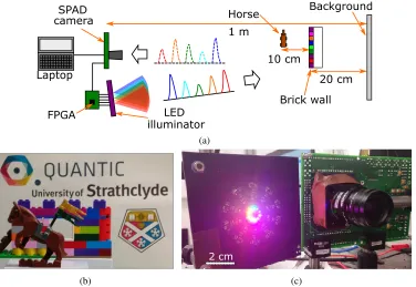
A top-down schematic of the experimental arrangement can be seen in Fig. 1(a). LED illumination is provided by an array of commercial LEDs, operated in a pulsed manner with each LED pulse on a different delay with respect to a trigger signal from the SPAD camera. Both LED array and SPAD camera are controlled with field-programmable gate array (FPGA) modules. Details and characterisation of the LED illuminator and camera can be found in the Appendix. To demonstrate measurement of varying visible reflectance spectra, a scene with many colours was constructed from Lego bricks. A photograph of the scene taken with a conventional camera is shown in Fig. 1(b). In order to show depth capability, a background plane with colour logos was positioned 1 m from the SPAD camera, with a brick wall 20 cm closer, and a horse minifigure a further 10 cm closer. The train of optical pulses emitted by the LEDs are reflected with intensities modified due to the reflectance characteristics of objects in the scene. Reflected pulses are captured by the SPAD camera and sent to a laptop via a USB3 connection to be processed. The timing functionality is performed on the SPAD chip, producing a single time-of-arrival value per frame for each pixel. The TCSPC histogram is constructed and analysed offline on the laptop.
1 m
20 cm 10 cm
Background
Brick wall SPAD
camera
LED illuminator
Horse
FPGA Laptop
(a)
(b)
2 cm
(c)
Fig. 1. (a) Top-down schematic of the experimental setup. (b) Image of the target scene taken with a conventional camera. (c) Photograph of the LED board and camera system. The LEDs are distributed in a 1 cm diameter ring.
Due to the time taken for photons to travel from the LEDs to the scene and back to the camera, the entire waveform will be shifted in time depending on the distance to the imaged object. As the scene used has depth variations on the order of 10 cm, the temporal shifts will be below 1 ns. On a 300 ns long, multi-pulse waveform with a histogram bin width of 642 ps and varying relative peak intensities, such a shift is a challenge to measure precisely. However, taking a reference histogram at a known distance, an example of which is also shown in Fig. 2(a), allows the time shift to be determined accurately by cross-correlation. The result of cross-correlating the example reference and image histograms is shown in Fig. 2(b). The peaks are still approximately 10 ns wide, however the time delay can be determined with improved precision by finding the centroid, or weighted mean, of the middle peak. In this case, a delay of 4.3 ns is determined, corresponding to a distance of 65 cm relative to the reference plane, which is 40 cm from the camera, resulting in a distance measurement of 105 cm. This particular example pixel is imaging the background in Fig. 1(a), which is 1 m away from the camera. This method provides sub-ns scale resolution of the time delay, despite the long pulse train and wide histogram bins, resulting in cm-scale depth resolutions, as demonstrated in the following results section. By performing this process on a pixel-by-pixel basis, a depth map can be determined across the scene. In addition, the cross correlation of measurement and reference signals automatically accounts for any systematic variation in the timing measurements introduced by signal propagation through the sensor. Such variations would cause the histograms in Fig. 2(a) to arrive at different times, depending on the pixel’s location in the SPAD array. However, because both reference and image histograms are affected equally, the relative time delay measurement is unchanged.
[image:3.612.121.497.92.351.2]-80 -60 -40 -20 0 20 40 60 80 Delay (ns)
0 0.5 1
Cross correlation (a.u.)
(b)
Cross correlation Middle peak centroid
0 50 100 150 200 250 300 350
Photon arrival time (ns) 0
0.5 1 1.5
Counts (normalised)
(a)
Reference Image
4.3 ns
Fig. 2. (a) Example received reference and image histograms for a single pixel of the SPAD camera. The image histogram has been vertically offset for clarity. (b) Cross correlation of the histograms in (a), with the middle peak centroid indicated. Note that the centroid value is determined with a higher precision than the bin width of the histogram. The time lag corresponds to a depth measurement.
0 50 100 150 200 250 300
Photon arrival time (ns)
0 50 100 150
Counts
536 1149 1619 1252 1034 302 1117 1104 1707
[image:4.612.137.464.106.301.2]Histogram 659 nm 632 nm 623 nm 597 nm 525 nm 498 nm 469 nm 445 nm 418 nm
Fig. 3. Example histogram with wavelength-assigned time bins indicated. Representative sums of counts within a time bin region are indicated above the histogram.
each LED based on a reference measurement, dictating which bins in the TCSPC histogram are associated with which illuminating LED, and therefore wavelength. Figure 3 shows an example histogramhbacross binsb. The bin ranges, denoted[lλ,rλ](left to right) for each wavelengthλ are shown as coloured bars. Measurements of relative reflectanceRλ, for a given wavelength λ, can be made through summation of photons arriving in the time windows[lλ,rλ]. The total number of counts received from a particular LED is indicated above the histogram. The values will depend on the reflectance of the imaged scene, the spectral sensitivity of the pixels, and the amount of light originally emitted by the LED. Therefore, a suitable correction factorαλmust
[image:4.612.129.480.380.493.2]Rλ=αλ rλ
Õ
b=lλ
hb. (1)
In this manner, the spectral information has been mapped to timing data, similar to the wavelength-time encoding of Reference [23].
As discussed above, the varying depth of the scene causes the full waveform to shift in time. This means the summation ranges[lλ,rλ], determined by a reference measurement, will
not produce accurate count values according to Eq. (1), as the pulse edges may be outside the windows when significant temporal shifts are present. However, as time delay is already calculated for the depth measurement, it can also be applied to the bin ranges. The nearest integer number of time bins equal to the time delay, denotedd, is applied to the reflectance calculation
to account for the histogram shift. Equation (1) therefore becomes:
Rλ=αλ rλ−d
Õ
b=lλ−d
hb. (2)
From Eq. (2) and the time delay calculation, spectral and depth information can be recovered from the same TCSPC histogram. With the arrayed SPAD camera system, this allows 3-D multispectral imaging.
3. Results
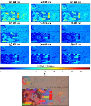
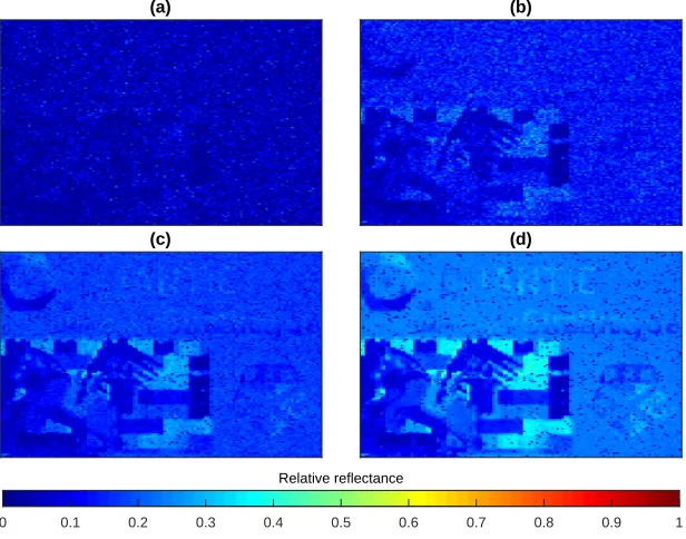
Images were reconstructed from the target scene by acquiring 10,000 TCSPC frames. Such a large number of acquisitions was chosen deliberately to avoid the Poissonian noise which will dominate in low photon-count images. Each frame is from an exposure of 1 ms, which covers many repetitions of the waveform as the trigger signal is sent every 320 ns. However, the SPAD sensor records timing information for only the first photon to arrive within the exposure [25]. Therefore, each frame consists of, at most, one timing measurement per pixel. The current FPGA implementation has not been optimised to use the maximum frame rate achievable with the chip (18.6 kfps [25]), and records at 480 fps. Therefore the 10,000 frame datasets shown here have an acquisition time of 21 s. A reference measurement was taken with a white sheet of paper placed 40 cm from the camera, for determining the time bin ranges and for the cross correlation process. Figure 4 shows the multispectral images taken of the target scene, and the example histograms used in Figs. 2 and 3 are from the same dataset. We refer to Fig. 1(b) for a reference image of the scene taken with a conventional camera. Figures 4(a) - 4(i) are the relative reflectance maps for each wavelength channel, specified by the LED wavelengths. It can clearly be seen by comparison with the reference image that the different coloured areas in the scene reflect more light in the expected channels, such as the intense reflection of red (659 - 623 nm) light by the bricks at the wall edge (Figs. 4(a)-4(c)). From the reflectance images, an approximation of an RGB colour image can be reconstructed from three channels as shown in Fig. 4(j). The “hot pixels” for this RGB image, where the SPAD pixels are firing continuously and producing meaningless data, have been replaced by interpolating the surrounding pixels. It should be emphasised that this colour image is for illustrative purposes only, and we cannot expect an ideal match between the two images as colour matching and reconstruction is a complex process [6, 26]. Most of the objects in the scene are well represented in the RGB image, with clear colour distinctions. The “Quantic” and “University of Strathclyde” text, although visible, is difficult to make out due to glare from the transmitter reflecting from the glossy printed ink. The recovered images all feature a random spread of dark pixels, caused by SPADs which are either non-functional or “hot-pixels”, which fire continuously and therefore record no useful data.
(a) 659 nm
0 0.1 0.2 0.3 0.4 0.5 0.6 0.7 0.8 0.9 1
Relative reflectance
(b) 632 nm (c) 623 nm
(d) 597 nm (e) 525 nm (f) 498 nm
(g) 469 nm (h) 445 nm (i) 418 nm
[image:6.612.134.479.91.496.2](j)
Fig. 4. Multispectral imaging of the scene in Fig. 1(b). (a) - (i) Relative reflectance images for each (respectively labelled) wavelength channel. (j) RGB approximation constructed from the 623, 525 and 445 nm channels with hot pixels replaced by interpolation. (k) Reflectance spectra for selected areas in the image, as identified by the labels inset.
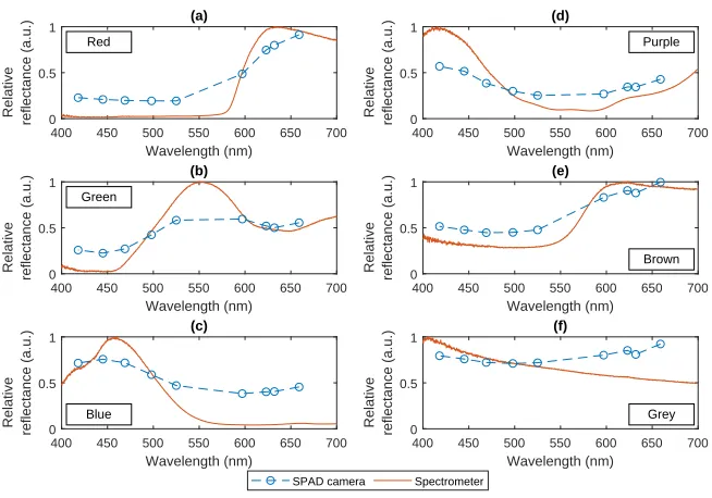
green brick, blue brick, purple brick, the horse and the saddle, respectively. For comparison, the spectra of each of the bricks was also measured using a commercial spectrometer (Avantes Avaspec-2048L) and halogen light source (Ocean Optics HL-2000-FHSA). The SPAD camera recovers the general trends of the spectra as expected, however, the ratio between high and low reflectivity portions of the spectra is reduced compared with the spectrometer results. Although the relative intensity of the different wavelength LEDs was used to calibrate the detector response, the variation in spectral width between the emitters was so far unaccounted for. These variations, and related overlap of the spectra of different emitters may contribute to this reduction in extinction ratio.
400 450 500 550 600 650 700
Wavelength (nm)
0 0.5 1
Relative reflectance (a.u.)
(a)
400 450 500 550 600 650 700
Wavelength (nm)
0 0.5 1
Relative reflectance (a.u.)
(b)
400 450 500 550 600 650 700
Wavelength (nm)
0 0.5 1
Relative reflectance (a.u.)
(c)
400 450 500 550 600 650 700
Wavelength (nm)
0 0.5 1
Relative reflectance (a.u.)
(d)
400 450 500 550 600 650 700
Wavelength (nm)
0 0.5 1
Relative reflectance (a.u.)
(e)
400 450 500 550 600 650 700
Wavelength (nm)
0 0.5 1
Relative reflectance (a.u.)
(f)
SPAD camera Spectrometer Blue
Green
Red Purple
[image:7.612.138.465.102.331.2]Grey Brown
Fig. 5. Coarse spectral data for various example areas within the image. (a) Red brick, (b) green brick, (c) blue brick, (d) purple brick, (e) horse, (f) saddle. A measurement with a spectrometer is included for comparison.
(a) 50 60 70 80 90 100 Depth (cm)
20 40 60 80 100 120
Horizontal pixel 50 60 70 80 90 100 110 Depth (cm) (b) 56 139 Truth 56 Truth 139 Vertical pixel
Fig. 6. (a) Depth map of the target scene. (b) Horizontal slices of the depth map. The standard deviation across row 139 is 3.41 cm
[image:7.612.129.487.385.509.2]the experimental setup. Shorter bin widths would permit more accurate depth measurements, but as the total number of bins is limited to 511, this would limit the full temporal range for the histogram, preventing the full 9 pulse waveform from being captured. Nevertheless, the standard deviation across the background line is 3.41 cm, well below the time bin resolution of 9.63 cm.
(c) (b)
0 20 40 60 80 100 120 140 160 180 200
Depth (cm) (a)
20 40 60 80 100 120
Horizontal pixel 20
40 60 80 100 120 140 160 180
Depth (cm)
(d)
0.5 m, map (a) 1.0 m, map (b) 1.5 m, map (c)
[image:8.612.142.462.164.421.2]0.5 m truth 1.0 m truth 1.5 m truth
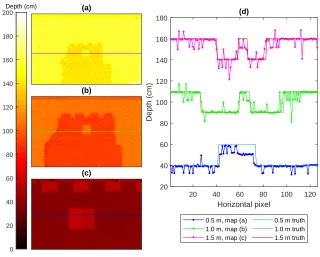
Fig. 7. Depth map performance at experimental distances of (a) 0.5, (b) 1.0 and (c) 1.5 m. Horizontal profiles through the depth maps are shown in (d), along with ground truth measurements.
To demonstrate that the depth imaging approach works over varying distances between the camera and target, measurements were taken at 0, 0.5 and 1.5 m distances. In each case, a background was placed a further distance of 10 cm from the camera, and the brick wall placed 10 cm closer. For example, in the 0.5 m case, the background was placed at 0.6 m, and the brick wall at 0.4 m. The resulting depth maps are shown in Fig. 7(a) - 7(c), for 1.5, 1.0 and 0.5 m respectively. Horizontal profiles through these maps are shown in Fig. 7(d), with the ground truth measurements for comparison. The performance at each of these ranges is very similar, with resolution strongly limited by the bin width and Poissonian nature of the approach, as discussed above. Range appears to have no significant effect on the performance. It can be seen that the measurement at a distance of 0.5 m exhibits increased a larger area within the window that cannot be accurately measured, as the shadowing from the brick wall reduces the number of received photons, as is also the case in Fig. 6.
4. Discussion
of the SPAD pixels. The number of spectral channels is also flexible, as increased numbers of LEDs simply requires a longer time window to collect TCSPC data. Conversely, fewer channels allows shorter acquisition times. Alternative transmitters such as lasers, RCLEDs, photonics crystal LEDs and superluminescent diodes may be of interest for narrower spectral line widths and could be applied to the same approach here, however the construction of a suitable illuminating array would have additional practical considerations, such as electrical driving, heat management and illumination optics.
(a) (b)
(c) (d)
0 0.1 0.2 0.3 0.4 0.5 0.6 0.7 0.8 0.9 1
[image:9.612.153.461.190.432.2]Relative reflectance
Fig. 8. Variation in image quality with (a) 10, (b) 100, (c) 1000, and (d) 10000 TCSPC frames for the 445 nm channel.
As mentioned in the results section, the SPAD sensor was operated at a frame rate of 480 Hz, resulting in an acquisition time of 20.83 s. Clearly this timescale is not suitable for video rate or high speed imaging. However, it first should be noted that the frame rate is currently limited by the control FPGA, and not the SPAD chip or experimental approach. A future system utilising high speed clocks for readout should achieve the 18.6 kfps frame rates possible for the SPAD chip [25], resulting in the same number of frames being captured in 0.54 s. Secondly, the acquisition of 10,000 frames is for demonstration purposes, to avoid the Poissonian noise of low photon count images. Acquisition times can be directly reduced by capturing fewer frames, though image quality will also be reduced. Figure 8 for example, shows the difference in image quality for the 445 nm channel (Fig. 4(h)) with fewer acquired frames. It can be seen that Fig. 8(a), with 10 frames, is dominated by noise, and the image is difficult to distinguish. However, the improvement in image quality between Figs. 8(c) and 8(d) is limited, despite the acquisition time increasing by a factor of 10. With the full chip frame rate of 18.6 kfps, video rate (30 fps) capture could be performed with 620 acquired TCSPC frames per video frame, which would provide an image quality between that of Figs. 8(b) and 8(c).
in-pixel counting and timing circuits. Nevertheless, it is highly likely that sensors with increasing resolution will be developed in the future. Recently, a 1024×8 line sensor was demonstrated with on-chip histogram capabilities [28]. Such an array could be used with the approach described here and using a line scanning system to achieve high resolution images.
0 5 10 15 20 25 30 35 40
Range (cm) 0
10 20 30 40
Measured range (cm)
Actual Measured
0 5 10 15 20 25 30 35 40
Range (cm) 1.0
0.5 0.0 0.5
Measured range residual (cm)
[image:10.612.178.419.165.366.2]Actual Measured
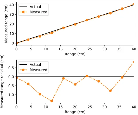
Fig. 9. Potential precision of the depth ranging when not limited by timing bin width.
The ranging resolution in the current experimental results is strongly limited by the TCSPC bin width of 642 ps, as this affects the resolution of the cross-correlation. This width is necessary as the timing counter has a maximum value of 511, and in order to capture the full pulse waveform, a minimum range of 300 ns is required. Finer bin widths should significantly improve ranging resolution, so it is important to consider the performance under the limitations of the approach rather than current hardware. Ranging experiments were performed using the same LED emitters and pulse trains, but with a single SPAD (Thorlabs SPCM20A) connected to a time-to-digital converter (TDC) module (Texas Instruments TDC7200). This allowed the same approach to ranging but with 55 ps resolution and no imaging capability. A series of measurements were made with a large, flat plane as a target at different ranges. The range measurement and residual are shown in Fig. 9. The standard deviation from the actual range is 0.64 cm, indicating a significant improvement in precision over the current imaging system. The TDC module has a timing resolution of 55 ps, corresponding to a depth resolution of 0.83 cm. As before, the standard deviation is below the expected resolution limit, indicating the cross-correlation and centroid processing produces improved depth measurements. Increased precision may be possible with shorter optical pulse widths. This could be achieved with laser emitters, or alternatively micro-LED systems [29], which would retain the advantages of simplicity, robustness and array format. In addition, as micro-LEDs are expected to become part of the next generation of display technology, it can be expected that full colour RGB arrays will be available, allowing this technique to be used to for 3D colour imaging.
5. Conclusion
400 450 500 550 600 650 700
Wavelength (nm)
0 0.5 1
Normalised power (a.u.)
Deep red
Red
Red orange
Amber
Green
Cyan
Blue
Royal blue
Violet
400 450 500 550 600 650 700
Wavelength (nm)
0 50 100
[image:11.612.181.433.96.238.2]Relative power (%)
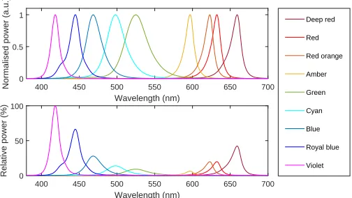
Fig. 10. Emission spectra of the LEDs used. Normalised (upper) and Received power relative to the maximum output of the violet LED (lower).
each wavelength given a specific time lag. The SPAD camera recovers TCSPC histograms for every pixel in the array, from which the amount of light received from each wavelength can be determined by the time-of-arrival of photons. Additionally, due to the time-of-flight nature of the approach, depth mapping is performed simultaneously. The experimental implementation has been demonstrated as able to distinguish spectra from a variety of colours within a scene while also showing a coarse depth measurement, well below that of the pulse width of the LEDs.
The underlying data for this work is available at:
https://doi.org/10.15129/5c4779bf-7d9c-4f21-a2fc-e6914f5af3cb
Appendix
SPAD camera
The SPAD image sensor used for this work is reported in [25], and consists of 192×128 SPAD pixels with dedicated timing electronics. Each pixel is 18.4×9.2 µm2 in area, and can be operated with TCSPC functionality, in which each pixel records the time-of-arrival for the first detected photon in an exposure period. Therefore each output frame consists of a time bin value for each pixel. Repeating this over many frames allows a histogram of arrival times to be built up in a pixel-wise manner, allowing 2-D imaged TCSPC to be performed. The image sensor is addressed and read out through an FPGA module (Opal Kelly XEM6310-LX150) with user control provided through a graphical user interface. The maximum possible frame rate of the chip is 18.6 kfps, however, the FPGA implementation for this work has not yet been optimised for speed, and the frame rate is limited to 480 fps.
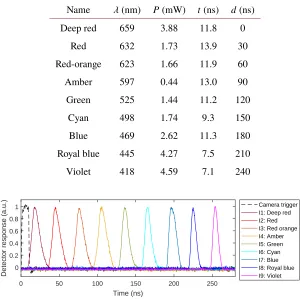
Table 1. Summary of LED characteristics. Peak wavelength (λ), average power (P), full width at half maximum (FWHM) pulse width (t) and delay time (d).
Name λ(nm) P(mW) t(ns) d(ns)
Deep red 659 3.88 11.8 0
Red 632 1.73 13.9 30
Red-orange 623 1.66 11.9 60
Amber 597 0.44 13.0 90
Green 525 1.44 11.2 120
Cyan 498 1.74 9.3 150
Blue 469 2.62 11.3 180
Royal blue 445 4.27 7.5 210 Violet 418 4.59 7.1 240
0 50 100 150 200 250
Time (ns) 0
0.2 0.4 0.6 0.8 1
Detector response (a.u.)
Camera trigger I1: Deep red I2: Red I3: Red orange I4: Amber I5: Green I6: Cyan I7: Blue I8: Royal blue I9: Violet
Fig. 11. Optical pulses from the LED array, measured with an APD. The response has been normalised for clarity, pulse intensity varies from one LED to another.
LED array
The structured illumination is here produced using LEDs, due to their simplicity, robustness and ease of integration into a 2D array. The LED array comprises of 9 commercially available LEDs (Lumileds Luxeon Z series) mounted on a PCB in a 1 cm diameter ring to minimise the difference in illumination angle between emitters. No optics were used in order to provide a reasonably uniform illumination across the target scene. The LEDs have an active area of 1 mm2
and a range of wavelengths covering the visible spectrum, chosen for demonstration purposes. The same approach can be used with any available LED wavelengths, provided they fall within the spectral response of the receiver, potentially enabling ultraviolet and infrared imaging.
200 300 400 500 600 700 800 900 1000
Wavelength (nm)
0 20 40 60 80 100
Reflectance (%)
0 400 800 1200 1600 2000
Counts
[image:13.612.190.436.99.208.2]Reference reflectance Median counts Calibrated counts
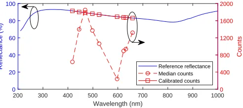
Fig. 12. Correction of the received counts from a known reflectance target.
Despite identical driving conditions, aside from the signal delay, the pulse width and average emitted power varies significantly from one LED to another, as efficiency and frequency response will vary with the semiconductor material and structure used to produce different wavelengths. In fact, the well known “green-gap” problem in semiconductors can be observed in the relative spectra of Fig. 10, where the green-yellow region shows significantly reduced emitted power. The variations in pulse width are accounted for when defining the time bin ranges[tb1(λ),tb2(λ)], and the emitted power variations can be dealt with through calibration.
Calibration process
In order to determine the spectral reflectance of a target from the number of received photons, it is important to perform a calibration process as there are a several other factors which will influence the number of counts. Firstly, the SPAD pixels have a wavelength dependent photon detection probability, with a peak around 500 nm, falling close to zero at 350 and 1000 nm [30]. Secondly, while the LEDs are all driven with short 5 V pulses, the optical emission varies strongly from one wavelength to the next, as seen in Fig. 10. Finally, the camera optics have significant variation in transmission with wavelength.
Calibration was performed experimentally by measuring a target with known reflectance across the desired spectrum. A diffuse reflector (Thorlabs DG10-120-F01) was used, with the reflectance spectra,Rλ,r e f, shown in Fig. 12 as a solid line. By comparing the measurement made with the SPAD camera to the known reference reflectance a calibration factor can be determined to correct the data. The reflector was arranged to fill a large part of the field-of-view of the SPAD camera and relative reflectance was calculated based on the methods described in Section 2. The mean reflectance values for the reflector,Rλ,mean, were calculated, so the calibration factorαλ can be determined by:
αλ= Rλ,r e f Rλ,mean
. (3)
Figure 12 shows the measured mean counts, and the calibrated counts indicating the correction factor reproduces the known spectrum.
Funding
Acknowledgments
We would also like to thank STMicroelectronics for chip fabrication, under the ENIAC POLIS project.
Disclosures
The authors declare no conflicts of interest.
References
1. N. Hagen and M. W. Kudenov, “Review of snapshot spectral imaging technologies,” Opt. Eng.52, 090901 (2013). 2. A. F. Goetz, G. Vane, J. E. Solomon, and B. N. Rock, “Imaging spectrometry for Earth remote sensing.” Science228,
1147–53 (1985).
3. Q. Li, X. He, Y. Wang, H. Liu, D. Xu, and F. Guo, “Review of spectral imaging technology in biomedical engineering: achievements and challenges,” J. Biomed. Opt.18, 100901 (2013).
4. G. Lu and B. Fei, “Medical hyperspectral imaging: a review,” J. Biomed. Opt.19, 010901 (2014).
5. J. Qin, K. Chao, M. S. Kim, R. Lu, and T. F. Burks, “Hyperspectral and multispectral imaging for evaluating food safety and quality,” J. Food Eng.118, 157–171 (2013).
6. D. H. Foster and K. Amano, “Hyperspectral imaging in color vision research: tutorial,” J. Opt. Soc. Am. A36, 606 (2019).
7. H. Liang, “Advances in multispectral and hyperspectral imaging for archaeology and art conservation,” Appl. Phys. A106, 309–323 (2012).
8. M. L. Nischan, R. M. Joseph, J. C. Libby, and J. P. Kerekes, “Active Spectral Imaging,” Lincoln Laboratory Journal 14, 131–144 (2003).
9. M. Parmar, S. Lansel, and J. Farrell, “An LED-based lighting system for acquiring multispectral scenes,” Proc. SPIE, Digital Photography VIII8299, 82990P–1 (2012).
10. H. N. Li, J. Feng, W. P. Yang, L. Wang, H. B. Xu, P. F. Cao, and J. J. Duan, “Multi-spectral imaging using LED illuminations,” 5th International Congress on Image and Signal Processing, CISP 2012 pp. 538–542 (2012). 11. S. Kim, D. Cho, J. Kim, M. Kim, S. Youn, J. E. Jang, M. Je, D. H. Lee, B. Lee, D. L. Farkas, and J. Y. Hwang,
“Smartphone-based multispectral imaging: system development and potential for mobile skin diagnosis,” Biomed. Opt. Express7, 5294 (2016).
12. J. Geng, “Structured-light 3D surface imaging: a tutorial,” Adv. Opt. Photonics3, 128 (2011).
13. A. Mansouri, A. Lathuilièere, F. S. Marzani, Y. Voisin, and P. Gouton, “Toward a 3D multispectral scanner: An application to multimedia,” IEEE Multimedia14, 40–47 (2007).
14. V. Paquit, K. Tobin, J. Price, and F. Meriaudeau, “3D and multispectral imaging for subcutaneous veins detection,” Opt. Express17, 11360–11365 (2009).
15. S. Heist, C. Zhang, K. Reichwald, P. Kühmstedt, G. Notni, and A. Tünnermann, “5D hyperspectral imaging: fast and accurate measurement of surface shape and spectral characteristics using structured light,” Opt. Express26, 23366–23379 (2018).
16. G. Nam and M. H. Kim, “Multispectral photometric stereo for acquiring high-fidelity surface normals,” IEEE Comput. Graph. Appl.34, 57–68 (2014).
17. R. Anderson, B. Stenger, and R. Cipolla, “Color photometric stereo for multicolored surfaces,” Proceedings of the IEEE International Conference on Computer Vision pp. 2182–2189 (2011).
18. G. Fyffe, X. Yu, and P. Debevec, “Single-shot photometric stereo by spectral multiplexing,” 2011 IEEE International Conference on Computational Photography, ICCP 2011 pp. 1–6 (2011).
19. A. M. Pawlikowska, A. Halimi, R. A. Lamb, and G. S. Buller, “Single-photon three-dimensional imaging at up to 10 kilometers range,” Opt. Express25, 11919 (2017).
20. D. D.-U. Li, J. Arlt, J. Richardson, R. Walker, A. Buts, D. Stoppa, E. Charbon, and R. Henderson, “Real-time fluorescence lifetime imaging system with a 32 × 32 0.13µm CMOS low dark-count single-photon avalanche diode array,” Opt. Express18, 10257 (2010).
21. D. D.-U. Li, J. Arlt, D. Tyndall, R. Walker, J. Richardson, D. Stoppa, E. Charbon, and R. K. Henderson, “Video-rate fluorescence lifetime imaging camera with CMOS single-photon avalanche diode arrays and high-speed imaging algorithm,” J. Biomed. Opt.16, 096012 (2011).
22. T. Hakala, J. Suomalainen, S. Kaasalainen, and Y. Chen, “Full waveform hyperspectral LiDAR for terrestrial laser scanning,” Opt. Express20, 7119 (2012).
23. X. Ren, Y. Altmann, R. Tobin, A. Mccarthy, S. Mclaughlin, and G. S. Buller, “Wavelength-time coding for multispectral 3D imaging using single-photon LiDAR,” Opt. Express26, 30146 (2018).
24. E. Charbon, “Single-Photon imaging in complementary metal oxide semiconductor processes,” Philos. Transactions Royal Soc. A372, 1–31 (2014).
26. H. Lee,Introduction to color imaging science(Cambridge University Press, Cambridge, 2005).
27. A. C. Ulku, C. Bruschini, I. M. Antolovic, Y. Kuo, R. Ankri, S. Weiss, X. Michalet, and E. Charbon, “A 512 × 512 SPAD image sensor with integrated gating for widefield FLIM,” IEEE J. Sel. Topics Quantum Electron.25, 1–12 (2019).
28. A. T. Erdogan, R. Walker, N. Finlayson, N. Krstaji, G. O. S. Williams, and R. K. Henderson, “A 16.5 Giga Events/s 1024 × 8 SPAD Line Sensor with per-pixel Zoomable 50ps-6.4ns/bin Histogramming TDC,” Symposium on VLSI Circuits pp. C292 – C293 (2017).
29. J. J. D. McKendry, B. R. Rae, Z. Gong, K. R. Muir, B. Guilhabert, D. Massoubre, E. Gu, D. Renshaw, M. D. Dawson, and R. K. Henderson, “Individually addressable AlInGaN micro-LED arrays with CMOS control and subnanosecond output pulses,” IEEE Photon. Technol. Lett.21, 811–813 (2009).