Laser cooled atoms are central to modern preci-sion measurements1–6. They are also increasingly important as an enabling technology for experi-mental cavity quantum electrodynamics7,8, quan-tum information processing9–11 and matter wave interferometry12. Although significant progress has been made in miniaturising atomic metro-logical devices13,14, these are limited in accuracy by their use of hot atomic ensembles and buffer gases. Advances have also been made in produc-ing portable apparatus that benefit from the ad-vantages of atoms in the microKelvin regime15,16. However, simplifying atomic cooling and load-ing usload-ing microfabrication technology has proved difficult17,18. In this letter we address this prob-lem, realising an atom chip that enables the inte-gration of laser cooling and trapping into a com-pact apparatus. Our source delivers ten thou-sand times more atoms than previous microfab-ricated magneto-optical traps and, for the first time, at sub-Doppler temperatures. Moreover, the same chip design offers a simple way to form stable optical lattices. These features, combined with the simplicity of fabrication and the ease of operation, make these new traps a key advance in the development of cold-atom technology for high-accuracy, portable measurement devices.
There have been rapid developments in quantum tech-nology since the first microKelvin atom traps19. Today many core experimental techniques can be realised us-ing atom chips16— microfabricated structures that trap, guide and detect ultra-cold atoms in a small integrated package. These offer the prospect of miniature, portable instruments based on the internal quantum states of atoms, with clocks being a good example. Bose-Einstein condensates can also be produced on a chip20, giving access to the quantum behaviour of the atomic motion for applications using phenomena such as matter-wave interference21,22 or spin entanglement23. Atom chips of-fer the tantalising prospect of portable setups, as
ultra-∗These authors contributed equally.
high-vacuum chambers24 and lasers for cooling in small packages are now available. However, the main obstacle to miniaturisation has been the lack of a simple inte-grated magneto-optical trap (MOT) to collect and cool the atoms initially and to load them onto the chip.
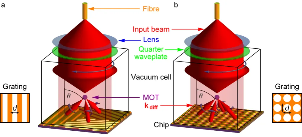
A MOT is formed near the zero of a quadrupole mag-netic field, located anywhere within the overlap region (Supplementary Section 1) of at least four appropri-ately polarised laser beams, slightly red-detuned from an atomic resonance19. A pyramidal reflector can produce the required beams from a single circularly-polarised input25, and such reflectors have recently been integrated into an atom chip17,18. However, the number of atoms captured is less than 7×10³ – far too low for appli-cations requiring degeneracy or where signal to noise is paramount. The atoms are also trapped below the chip surface, making them inconvenient to access and detect. We present a new atom chip MOT that delivers 6×10⁷ atoms in a readily accessible trap, representing a 104-fold atom number improvement over current single-beam chip traps. Reflection gratings, microfabricated on the chip surface, transform a single input beam into several suit-ably polarised beams that form a MOT when combined with a magnetic quadrupole26,27. For example, Fig. 1a shows three linear gratings producing a tetrahedral con-figuration of beams, while Fig. 1b shows a square lattice of cylindrical indentations making a five-beam arrange-ment. The diffraction angle θ depends on the wave-length λ of the light and the period d of the grating through the Bragg conditionsnxλ=dsinθ(linear) and
√
nx2+ny2λ=dsinθ(square).
FIG. 1: Concept of the grating chip MOT.Linearly-polarised light (red) diverging from the output of an optical fibre (orange) is collimated and circularly polarised (grey arrow) by the combination of a lens (blue) and quarter-wave plate (green). This single input beam diffracts from microfabricated gratings on the chip to produce the additional beams (small red arrows indicate wave-vectors,kdiff) needed to form a MOT. The light traps atoms from a low-pressure vapour inside an evacuated glass
[image:2.595.78.551.389.486.2]cell, see Methods. aThree linear gratings (pattern shown inset) diffract the light into thenx=±1 orders to form a 4-beam MOT (only trapping beams are shown). bA square array of cylindrical indentations (pattern shown inset) diffracts the input into thenx=±1 andny=±1 orders to form a 5-beam MOT. The retro-reflections (nx, ny= 0) are strongly suppressed and higher orders of diffraction are eliminated (see Methods). Magnetic quadrupole coils are omitted for clarity.
FIG. 2: The grating chips. aPhotograph of chip A which consists of three linear 8 mm×8 mm gratings of pitchd= 1200 nm (θ= 41◦). Inset: scanning electron microscope (SEM) image showing the cleaved cross section through the coated grating. b
Chip B extends the pattern of chip A inward to the centre and outward over a 20 mm×20 mm area. The SEM image shows the centre of the mask, which has a pitch ofd= 1400 nm (θ= 34◦). Inset: SEM close-up of the etched and coated chip surface.
cChip C is an array of squares covering a total area of 2 cm×2 cm, with a pitch ofd= 1080 nm (θ= 46◦). An SEM image of the mask is shown, together with a zoomed image, inset. dChip D is the same as C, but with the squares replaced by circles.
have to be protected from collisions with background gas. Our chips can be operated in a UHV chamber but they can also be used outside, with a vacuum window between the surface of the chip and the cold atom cloud. All four chips have been tested in this simple configuration, using a single input laser beam.
The number of atoms trapped in a MOT depends on the beam overlap volume, as well as the laser frequency and intensity. Figure 3a shows the number of87Rb atoms trapped by each chip from a low-pressure vapour as the laser frequency is varied. The detuning, which optimises
ôôôôôôôôôôôôôôôôôôôôôôôô
ôôôôôôôôôôôô
õõõõõõõõõõõõõõõõõõõõõõõõ
õõõõõõõõõõõõ òòòòò
ò òòò
òòòòò òòòòòòò
óóóóó
ó óóó
óóóóó óóóóóóó
æ æ
ææ
ç ç
çç ì
ìì
í íí
-2.5 -2.0 -1.5 -1.0 0
1
DetuningDG
[image:3.595.51.549.49.194.2]Atom
FIG. 3: Variation of atom number with laser detuning and intensity.aNumber of atoms trapped by each chip as the detuning was varied, measured in units of natural linewidth Γ = 2π×6 MHz. For each curve a fixed intensity, which optimised the atom number, was used. Data points are the average of 5 runs, resulting in statistical uncertainties much smaller than the plot markers. The atom number peaks at a detuning around two linewidths below resonance, which is typical for most MOTs. Inset: Fluorescence of trapped atoms above chip D at maximum atom number. bAtom number versus detuning and input beam peak intensity using chip D, obtained using the detunings inaat 11 additional intensities and interpolating a surface.
trapped. Chip B collects three times as many atoms as chip A because its diffracted beams have larger cross sec-tion, producing a larger trap volume and hence capturing faster atoms18,28. Chips C and D capture three times as many atoms again, because this geometry has a differ-ently shaped and larger overlap volume (Supplementary Section 1).
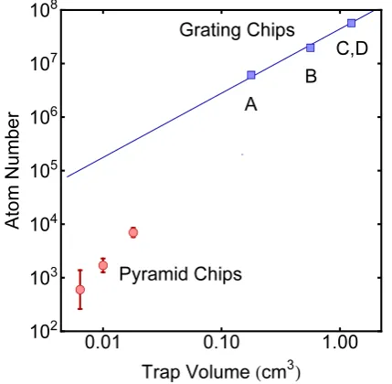
We have investigated the atom number scaling on our grating chips, and find a factor of 104improvement com-pared with previous microfabricated chip traps. In Fig. 4 we plot the peak number of trapped atoms N for each
FIG. 4: Variation of peak atom number,N, with trap-ping volume,V. Blue squares: number of atoms trapped by each of the grating chips A-D. Red circles: numbers trapped by microfabricated pyramid chips18. Where error bars are not visible, they are much smaller than the data points.
chip versus the trap volume V. The trap dimensions are large enough to follow the approximate scaling law28 N∝V1.2, indicated by the blue line in Fig. 4. The max-imum number of atoms captured by grating Chip D is 6×10⁷, essentially the same as a conventional six-beam MOT of the same volume (see Methods). By contrast, the pyramid MOT of Pollocket al.18, the only other mi-crofabricated MOT in the literature, follows aV2power law because of its small volume, capturing to date a max-imum of 7×10³ atoms as indicated in Fig. 4 by the red points.
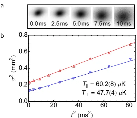
For many applications, such as the production of quan-tum degenerate gases, sub-Doppler temperatures are im-portant in order to obtain high phase space densities. We have demonstrated that our chips can reach this regime. The initial temperature of atoms trapped on our chips is
[image:3.595.70.285.446.656.2]a
[image:4.595.58.283.49.242.2]b
FIG. 5: Temperature measurements on chip B.a Se-quence of fluorescence images (2.7 mm×2.7 mm) taken during ballistic expansion, after optical molasses. b Mean square cloud radii parallel (red upward triangles) and perpendicu-lar (blue downward triangles) to the grating, versus square of expansion time t. Error bars are smaller than the size of a point. Lines: fits ofσ2=σ2
0+
kBT
m t
2to the data, wherekBis
the Boltzmann constant, T is the temperature and mis the mass of an 87Rb atom. Anisotropic expansion of a molasses is not unusual.
There is a fixed relative phase between the diffracted beams, referenced to the chip surface. This ensures a stable, periodic interference pattern of intensity and po-larisation that requires no user alignment. In this way, an input light beam diffracting from anywhere on grating chips C or D automatically creates a three-dimensional body-centred-cubic lattice of microscopic atom traps which, for suitable far red-detuned light, localises atoms in intensity maxima due to the optical dipole force. Op-tical lattices are already well established as a valuable technique in atomic clocks1 and quantum simulators30. Our gratings open the possibility of introducing lattices in a simple way to atom chips.
In conclusion we have demonstrated how a MOT can be incorporated into atom chips with the use of microfabricated optical gratings, illuminated by a single laser beam. We have shown that our MOT traps
N ∼ 108 atoms, with potential for increased number for larger chip sizes. Moreover, the chip MOT can also be switched to an optical molasses which provides sub-Doppler cooling. Our MOTs provide a key element for integrated architectures that was previously missing and opens the way for truly portable devices to be built on atom chips through a radical reduction of the footprint and simplification of the optical setup. In addition, the gratings offer a simple and stable way to introduce 3D optical lattices onto chips, dramatically extending the functionality of future portable atomic
technologies.
Methods
Chip fabrication. We etched patterns to a depth of λ/4
(λ = 780 nm), with an approximately 50:50 etched:unetched area ratio, in order to suppress zeroth-order diffraction (reflection). For all the chips, this gave less than 1% of the incident power in the zeroth-order. The first order diffracted beams are described below for each chip. In all cases over 96 % of the diffracted power had the correct polarisation for MOT operation. Higher diffraction orders are cut off becaused≤2λfor the linear gratings andd≤√2λfor the square gratings.
Chip A:Fabricated in silicon using reactive ion etching (RIE).
The groove depth was measured to be 210 (10) nm using an atomic force microscope (AFM). To achieve high reflectivity, this chip was sputter coated with 200 nm of gold, following a 10 nm adhesion layer of chromium. We measured 40(1)% of the incident light in each of the first order diffracted beams.
Chip B: Fabricated in silicon using RIE. The AFM measured
a groove depth of 206 (10) nm. With a 3 nm nickel-chromium adhesion layer, and a 100 nm aluminium reflection coating we measured 38(1)% of incident power in each first order diffracted beam. With the additional diffracted beam losses due to two uncoated glass surfaces in the cell, this chip is close to the ideal 1/3 diffraction efficiency required for optimally balanced light forces in optical molasses27.
Chips C and D:Fabricated in silicon or gallium-arsenide. The
silicon chips had the same groove depth as chip B. For the gallium arsenide versions an etch stop was used to ensure a uniform depth of 195(5) nm. The same reflective coating as B was used for both. We found very little difference in the optical behaviour of the coated Si and GaAs chips. Both varieties were tested inside and outside the vacuum chamber and had comparable performance. The data shown in this letter is from the silicon chips. We measured that 20(1)% of the incident power was diffracted into each of the four first order beams.
Vacuum, magnetic fields and imaging. All
experi-ments used an externally anti-reflection coated quartz vacuum chamber with inner dimensions 22×22×80 mm3. A base pressure
<10−9mbar was maintained by a 40 l/s ion pump. A rubidium
partial pressure < 5 ×10⁻⁹mbar was regulated by a metal dispenser. The magnetic quadrupole coils, aligned coaxially with the chip normal, were operated with an axial gradient of 10 G/cm. Three orthogonal pairs of Helmholtz coils cancelled the ambient magnetic field. The MOT fluorescence was viewed using a CCD camera placed 10 cm from the atoms, with an imaging system with transverse magnification of 0.80.
Optics and laser system.Two external cavity diode lasers were
frequency stabilised on the87Rb D2 line using saturated
absorp-tion spectroscopy. One was locked to theF = 1 →2 hyperfine transition required for repumping. The other was locked with a red detuning of 0−33 MHz relative to theF = 2→3 hyperfine transition. The latter injected a slave laser that produced up to 20 mW of cooling light. This was combined with the repumping light on a beam splitter, linearly co-polarised and coupled into a single-mode optical fibre. A fibre-coupled tapered amplifier provided optical gain up to a total power of 500 mW. Its fibre output, shown in Fig. 1, was collimated to form a Gaussian beam of 20 mm 1/e2 intensity radius, and circularly polarised using a
Acknowledgements
We acknowledge EPSRC for support, C.N.’s Knowledge Transfer account and J.C.’s support fund. Also, the ESA through ESTEC project TEC-MME/2009/66, the CEC FP7 through project 247687 (AQUTE) and the Wellcome Trust (089245/Z/09/Z). P.G. is supported by the Royal Society of Edinburgh and E.H. by the Royal Society. We thank P. Edwards for his assistance with the SEM insets in Fig. 2a and 2b. All other SEM images in Fig. 2 are courtesy Kelvin Nanotechnology Ltd., who fabricated chips B-D at the James Watt Nanofabrication Centre. We also thank J. P. Griffith and G. A. C. Jones for assistance with GaAs e-beam lithography.
Author contributions
C.N., M.V., P.G., E.R. and A.A. constructed and maintained the apparatus. C.N., J.C. and A.A. took the data which was analysed by J.C. and A.A. Chip A was designed by J.C. and E.H. Chips B-D were designed by E.R. and A.A. with fabrication directed by P.S., A.S. and C.I. The manuscript was written by J.C., E.H. and A.A. with comments from all authors.
[1] Takamoto, M., Hong, F.-L., Higashi, R. & Katori, H. An optical lattice clock.Nature435, 321-324 (2005). [2] Deutsch, C. et al. Spin self-rephasing and very long
co-herence times in a trapped atomic ensemble.Phys. Rev. Lett.105, 020401 (2010).
[3] Buning, G. K. et al. Extended coherence time on the clock transition of optically trapped rubidium.Phys. Rev. Lett.106, 240801 (2011).
[4] Bodart, Q.et al. A cold atom pyramidal gravimeter with a single laser beam.Appl. Phys. Lett.96, 134101 (2010). [5] Poli, N.et al. Precision measurement of gravity with cold atoms in an optical lattice and comparison with a classi-cal gravimeter.Phys. Rev. Lett.106, 038501 (2011). [6] Lamporesi, G., Bertoldi, A., Cacciapuoti, L., Prevedelli,
M. & Tino, G. M. Determination of the Newtonian grav-itational constant using atom interferometry.Phys. Rev. Lett.100, 050801 (2008).
[7] Specht, H. P.et al. A single-atom quantum memory. Na-ture 473, 190-193 (2011).
[8] Ritter, S.et al. An elementary quantum network of single atoms in optical cavities.Nature484, 195-201 (2012). [9] Bakr, W. S.et al. Probing the superfluid-to-Mott
insu-lator transition at the single-atom Level. Science 329, 547-550 (2010).
[10] Sherson, J. F. et al. Single-atom-resolved fluorescence
Phys. Lett. 85, 1460-1462 (2004); actual products at www.symmetricom.com.
[14] Shah, V., Knappe, S., Schwindt, P. D. D. & Kitching, J. Subpicotesla atomic magnetometry with a microfabri-cated vapour cell.Nature Photonics 1, 649-652 (2007). [15] van Zoest, T.et al. Bose-Einstein condensation in
micro-gravity.Science 328, 1540-1543 (2010).
[16] Reichel, J. & Vuleti´c, V., eds.Atom Chips(Wiley, 2011). [17] Pollock, S., Cotter, J. P., Laliotis, A. & Hinds, E. A. Inte-grated magneto-optical traps on a chip using silicon pyra-mid structures.Opt. Express 17, 14109-14114 (2009). [18] Pollock, S., Cotter, J. P., Laliotis, A., Ramirez-Martinez,
F. & Hinds, E. A. Characteristics of integrated magneto-optical traps for atom chips. New J. Phys. 13 043029 (2011).
[19] Raab, E. L., Prentiss, M., Cable, A., Chu, S. & Pritchard, D. E. Trapping of neutral sodium atoms with radiation pressure.Phys. Rev. Lett.59, 2631-2634 (1987). [20] H¨ansel, W., Hommelhoff, P., H¨ansch, T. W. & Reichel,
J. Bose-Einstein condensation on a microelectronic chip.
Nature413, 498-501 (2001).
[21] Schumm, T.et al. Matter-wave interferometry in a dou-ble well on an atom chip.Nat. Phys.1, 57-62 (2005). [22] Baumg¨artner, F. et al. Measuring energy differences by
BEC interferometry on a chip. Phys. Rev. Lett. 105, 243003 (2010).
[23] Riedel, M. F.et al., Atom-chip-based generation of entan-glement for quantum metrology.Nature464, 1170-1173 (2010).
[24] http://www.coldquanta.com
[25] Lee, K. I., Kim, J. A., Noh, H. R. & Jhe, W. Single-beam atom trap in a pyramidal and conical hollow mirror.Opt. Lett.21, 1177-1179 (1996).
[26] Vangeleyn, M., Griffin, P. F., Riis, E. & Arnold, A. S. Single-laser, one beam, tetrahedral magneto-optical trap.
Opt. Express 17, 13601-13608 (2009).
[27] Vangeleyn, M., Griffin, P. F., Riis, E. & Arnold, A. S. Laser cooling with a single laser beam and a planar diffractor.Opt. Lett.35, 3453-3455 (2010).
[28] Lindquist, K., Stephens, M. & Wieman, C. E. Experi-mental and theoretical study of the vapor-cell Zeeman optical trap.Phys. Rev. A46, 4082 (1992).