Development and simulation of soft
morphological operators for a field
programmable gate array
Development and simulation of soft morphological
operators for a field programmable gate array
Andrew J. Tickle Coventry University
Department of Aerospace, Electrical, and Electronic Engineering Priory Street Coventry CV1 5FB, United Kingdom
E-mail:[email protected]
Paul K. Harvey Jeremy S. Smith Q. Henry Wu University of Liverpool
School of Electrical Engineering, Electronics, and Computer Science Brownlow Hill Liverpool L69 3GJ, United Kingdom
Abstract. In image processing applications, soft mathematical mor-phology (MM) can be employed for both binary and grayscale sys-tems and is derived from set theory. Soft MM techniques have improved behavior over standard morphological operations in noisy environments, as they can preserve small details within an image. This makes them suitable for use in image processing applications on portable field programmable gate arrays for tasks such as robotics and security. We explain how the systems were developed using Altera’s DSP Builder in order to provide optimized code for the many different devices currently on the market. Also included is how the circuits can be inserted and combined with previously developed work in order to increase their functionality. The testing procedures involved loading different images into these systems and analyz-ing the outputs againstMATLAB-generated validation images. A set of soft morphological operations are described, which can then be applied to various tasks and easily modified in size via alter-ing the line buffer settalter-ings inside the system to accommodate a range of image attributes ranging from image sizes such as
320×240pixels for basic webcam imagery up to high quality
4000×4000pixel images for military applications.© 2013 SPIE and IS&T [DOI:10.1117/1.JEI.22.2.023034]
1 Introduction
This paper continues the research described in Refs.1and2, whilst still using the methodologies presented in them to implement the circuitry/algorithms and give them greater noise immunity to make them more robust. The system was designed in order to allow the k-value, as it is called here, to be easily changed without the internal setting having to be changed. Thisk-value is what gives the system its noise immunity. Whenk¼1, the system will operate in the same way as standard morphological operations (MO), but as this value is increased, the noise immunity is subsequently increased but at the cost of losing some of the image
data. One target application of this work can be soft morpho-logical operation (SMO) filters, which are a combination of standard MO filters and a weighted rank order filter,3,4 hav-ing the potential for very high performance image process-ing. Other possible applications include using mathematical morphology (MM) to remove noise to improve the quality and performance of automated imaging systems. These include tracking for example,5,6 by effectively removing
the data that is not required in the background or the noise in the foreground better than standard MOs. These processes could further assist in encryption and application specific systems developed for field programmable gate arrays (FPGA) using this methodology in conjunction with hand-written code.7–10 As with previous systems,
there will be two 3×3 pixel structuring element (SE) cases used to perform this work on 640×480 imagery. These circuits are able to compute the output image files for a given input file with a given k-value in one time step per pixel. In order to save time and resources during the advanced calculations of a single k-value, it would be wise to perform these operations with a single pass, rather than a cascaded effect of erosion and dilation or vice versa.11 Without the single step operation, it would require two processing passes for one advanced operation (either opening or closing), which produces a delay in the filtering process and limits the speed at which the system can be run. This cascaded process requires large amounts of memory in order to store the intermediate result, which is why the cas-cade effect is not an efficient method since the programmable interconnects and memory on an FPGA is limited.
These SMOs allow the user to perform cascaded opera-tions in the previous multifunctional system with different
k-values, which was one of the reasons why the system pre-sented in Ref.2 was designed that way. Presented in this paper are the optimal system configurations and layouts, while briefly discussing the alternatives and the reasons why they were not suitable for the applications at hand. Many computer vision applications can benefit from the inte-gration of image capture and image processing functions Paper 10053 received Aug. 22, 2010; revised manuscript received Aug. 6,
2012; accepted for publication Apr. 29, 2013; published online Jun. 25, 2013.
onto an FPGA by describing the gate level implementation in a layered structure in order to reduce delays and to aid in debugging operations.12,13 The two main layouts were a multi-k SMO system and a separated-k SMO system. With the multi-k system, all the data goes into one block and all copies and pixel values are ranked and sorted before being correctly output to the right ports. The separated-k
SMO system, on the other hand, has a block which performs each k-value operation separately in a parallel processing architecture14rather than a single block system. An overall decision block then decides which signals are output based on thek-value input via the user whilst the remaining signals are terminated. A size comparison also takes place where the circuits from Ref.1are compared to the ones developed in this paper to determine if they take up more, less, or roughly the same amount of gates as the previous systems. This com-parison will also indicate whether the systems can still be synthesized onto an FPGA or not, it also provides an idea of the robustness of the SMOs against the MOs as whenk¼
1 the output from both these systems should be the same. Furthermore, the size of the developed circuitry should try to be as close as possible to the ones from Ref. 1 so that thek-value can be varied to higher values to provide greater noise immunity without the associated proportional increase in the size and complexity of the circuitry. A pixel-by-pixel analysis is also performed on the images and the results from noisy images are also discussed. The latter were passed through the system to investigate how noise affects the results and the comparison process. The work here is to present the most basic SMOs at the two most commonly used levels/dimensions so that work can then continue
into the more advanced SMOs and their associated systems and applications.
Section 2 presents the mathematical morphology (MM) theory which is structured into circuitry and described in Sec. 3. Computational complexity, effectiveness of the circuit operations, and size comparisons are analyzed in Sec.4, whilst conclusions are drawn in Sec. 5.
2 Soft Morphological Operations
Here, the SE is divided into two parts: the core which has a weight or number of copiesk(repetition parameter) which can be equal to or greater than “1”and the soft boundary which acts in the same way as the pixels in a standard MO structuring element. This is defined mathematically as the core and the soft boundary of the SE Bby B1 and
B2, respectively, B¼B1 ∪B2. It has been proven that
soft morphological operations are advantageouvs regarding additive noise elimination and sensitivity to small variations in object shape when compared to standard morphological transforms.3,11 The shape for SE4 (a 4-connectivity SE which is defined in Ref.1) is shown where the bold numbers represent the core of the SE. Their corresponding pixel val-ues are also shown here:
SE 4¼
2
401 11 01 0 1 0
3 5¼
2
4Pixel 1Pixel 4 Pixel 2Pixel5 Pixel 2Pixel 6 Pixel 7 Pixel 8 Pixel 9
3 5: (1)
2.1 Binary Erosion
Binary soft erosion is defined as follows,15where Card½X
represents the cardinality or number of elements of the setX:
ðA⊖B1; B2; kÞðxÞ ¼
1 ifðk:Card½A∩ðB1Þx þCard½A∩ðB2Þx≥k:Card½B1 þCard½B2−kþ1Þ
0 Otherwise . (2)
Equation 2 states that in order to softly erode a binary image set A by a binary SE B, the SE is moved over the image set applying a standard MO. At each point x, the pixel intersection of A is a“1”with the translated core B1
must be found and multipliedktimes, then added to the car-dinality of the intersection ofAwith the translated soft boun-daryB2. The same operation is performed for the right-hand
side of the equation. If this result is greater than or equal to
k:Card½B1 þCard½B2−kþ1then the output pixel for that
3×3 pixelsegment is a“1.”There is some more information and examples of this process in Ref.16.
2.2 Binary Dilation
The process for binary soft dilation is very similar to erosion apart from the equation for the operation, which now becomes:
ðAB1; B2; kÞðxÞ
¼
1 ifðk:Card½A∩ðB1Þx þCard½A∩ðB2Þx≥kÞ
0 Otherwise :
(3)
2.3 Grayscale Erosion
Here,k⋄xdenotes thek-times repetition ofx. The core and the soft boundary of the SEgðzÞare denoted byαðzαÞand
βðzβÞ, respectively:
zα∈D½α; zβ∈D½β ¼D½g∕D½α; (4)
whereD½g∕D½αdenotes the set difference. The soft erosion offby a SEgwith a coreα, and a soft boundaryβis defined in Ref.16:
ðf⊖½β;α; kÞðxÞ ¼minkðk⋄ff½z
1−aðz1−xÞg ∪f½z2−βðz2−xÞÞ (5)
z1−x∈D½α (6)
z2−x∈D½β ¼D½g∕D½α; (7)
wheremink is thek’th smallest of the multiset in the
repetition is allowed. In order to grayscale soft erode an image set f by a SE g, the SE is moved over the image set as described previously, finding all the differences of the values offwith their corresponding values of the trans-lated coreα, after which all the differences of the values off
with the corresponding values of the translated soft boundary
βare produced. The resulting values are ranked in ascending order including thekcopies of the coreαand thek’th small-est is selected as the result.
2.4 Grayscale Dilation
The soft dilation offby an SEgalso with coreαand soft boundary β is defined in Ref.16:
ðf ½β;α; kÞðxÞ ¼maxkfk⋄½fðz
1Þ−aðx−z1Þ
∪fðz2Þ−βðx−z2Þg (8)
x−z1∈D½α (9)
x−z2∈D½β ¼D½g∕D½α; (10)
where maxk is now the k’th largest of the multiset in the
parentheses. The soft dilation offbygis translated spatially in the reflection ofg,gð−zÞ, so that it is located at the starting
point, after which the same steps are followed as in the soft erosion case, apart from the answer now producing thek’th highest instead of lowest.
2.5 Soft Opening and Closing
Soft opening and soft closing for both binary and grayscale systems are defined in Ref.5:
f∘½β;α; k ¼ ðf⊖½β;α; kÞ ½β;α; k (11)
f·½β;α; k ¼ ðf ½β;α; kÞ⊖½β;α; k: (12)
As with the standard morphological operations, the soft opening is a dual to soft closing and vice versa, but now unlike standard opening and closing they are neither exten-sive nor anti-extenexten-sive. In general, both soft opening and soft closing are not idempotent, and it has been proven that soft opening and closing are idempotent only under specific con-ditions. For example, in the case that g¼gS, the core
includes only one pixel which is located at the origin.16
3 Development of Systems 3.1 Binary Soft Morphology Circuitry
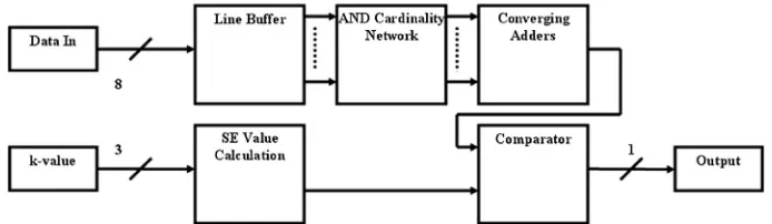
The system was designed so that thek-value is a constant throughout the system and therefore does not change. Figures1and2show two levels of abstraction for the binary system. The inputs and outputs of Fig.1, on the left and right, respectively, show the data input, clock, global reset, andk -value input. These would be the inputs and outputs of the system at the behavioral level. Also shown is the represen-tation of the signals being directed to the erosion calculator, dilation calculator, and data validator blocks, while Fig. 3 shows the basic layout of the dilation and erosion calculators. The SE value calculation block is the only section of this circuit which changes between the two systems, as this rep-resents the RHS (right-hand side) of Eqs. (3) and (4).
The two calculator circuits start by having the3×3image buffers which delay the image set in order to produce the3× 3image segment that the SE would move over if this were calculated by hand.1The soft pixel part of the SE is sent into
a series ofANDgates with a“1”going into the other input port so that if the input from the image segment is also a“1,”then the output from theANDgate will be a“1”and help calculate the cardinality of the soft part of the SE. Thus, this is theAND cardinality block. These outputs are then added together using three layers of adders (converging adders block) before a final adder adds the k-value to this in order to take into account the cardinality of the core of the SE. This latter value is obtained by sending the signal for pixel 5 from the image buffer into a product block, which is linked to the k-value input. So if pixel 5 is a “1” then the product will output thek-value to be added but if it is “0”then a
Fig. 1 Register transfer level (RTL) model for the binary system.
[image:4.630.141.488.632.733.2]“0”will be output instead. Finally, this total value is then sent into a comparator and compared with the SE value calcula-tion block output which, if greater than“1,”defines the result as “1”otherwise a“0”is the result.
The SE value calculation block of the system either adds the number of soft output pixels which comes from a con-stant block in order for them to be more easily changed (sim-ilarly from SE8 (an 8-connectivity SE, defined in a similar manner to SE4) to SE4 by changing the constant from an“8” to a“4”) to thek-value which represents the core. This is then added to a“1”value and then thek-value is subtracted for the erosion case whereas for dilation, thek-value is sent directly to the comparator at the end.
3.2 Grayscale Soft Morphology Circuitry
The behavioral level for the grayscale system is virtually identical to the binary system apart from the output data
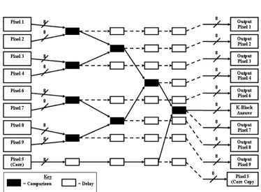
line widths having been expanded to 8 bits in order to account for the grayscale values that will be dealt with. Figures 3–5 show the register transfer level (RTL) and gate levels of abstraction for the grayscale system for the sep-arated-k SMO system, where Fig. 3 shows the series of blocks moving from left to right, which calculates the
k¼1 tok¼7 values, respectively, and sends them to the decision-maker block. In this block the correct k-value is finally output based on thek-value input into the system. The first block is an image buffer1that is modified slightly so that a“1”is either added or subtracted to all pixels in the image segment. In addition to this, a check was also added in order to prevent overflow so that a“1”would not be added or taken away if the value were“255”or“0,”respectively. This was accomplished by using a standard DSP Builder compa-rator to see if the value matches one of these values and if it does match, a“1”will be produced. It will then be inverted using aNOTgate and fed into anANDgate with a constant of
Fig. 3RTL model for the grayscale system.
[image:5.630.114.516.282.429.2] [image:5.630.127.501.456.731.2]“1”going in, so when they do not match they would both be
“1”s and so the output from theANDwould be a“1”which would then be added or subtracted, respectively. If they match however, the inputs to the ANDwould be a “1”and
“0,”respectively, so that a“0”is produced and no changes occur.
Figure4shows the basic layout of the dilation and erosion calculators in which the main elements of the system are based around the bus comparator, previously developed in Ref. 1 but now working in pairs where one would find the highest, while the other finds the lowest. The reason for this is that the system finds the highest or lowest value through a process of comparisons, then outputs the highest or lowest (depending on the operation) as the answer. However, the values which were not the highest nor the low-est need to be retained which is why the opposite operation is used in order to do this so that these values can be passed onto the next block along with a copy of the core. This effec-tively removes the highest or lowest value pixel and so the same block can be repeatedly used for the differentk-values instead of having to find the second highest, third highest, etc. and have a separate block for each. If the highest is removed, then when the process is repeated, the second high-est will obviously now become the highhigh-est. The other single comparator blocks (the delay blocks shown in Fig. 4) are there to ensure that all signals remain in synchronization with each other, such that propagation delay does not cause a major problem. These values are then sent to the next block relative to the last block, which is just a simple conversion with no need to output the nonhighest or lowest values.
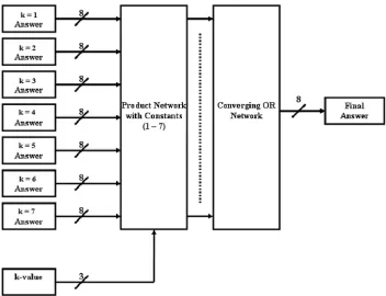
Figure 5 shows the decision-maker that decides which output from each of the possible seven k-value answers is in fact the true answer. There are the seven inputs from
the various blocks in the system which are each sent into a product block and the other input is from a comparator. These have constants ranging from 1 to 7 for the respective
k-value signals, and are compared to the actualk-value so the matching signal will produce a “1” from the comparator. When sent into the product, the output value is fed into an OR gate network which takes the signal to the output port. When the output from the comparator is a “0,” no value is sent out from the product block into theORnetwork, so it would not corrupt the true output value.
Overall, the separated-k SMO system is better than the multi-k SMO system because the separated blocks are smaller in size, less complicated, and less likely to have propagation signal errors in the output. The multi-ksystem had a series of nine blocks to find the first, second, third, etc. highest pixels and the number of copies of that pixel value. These were found by a process of comparisons to find the highest or lowest value, and then this result is compared to all pixel values to see how many other pixels also share that value, then the sum is computed and the data is output to the ranker. Eventually, all the pixel values would be “0” and the system will stop. A location signal was also sent out so that the system would know where and how to reconstruct the image segment. The ranker is also a complex piece of circuitry with over 120 possible combinations, so as a result the output was prone to propa-gation delay and dithering. The incoming signals had to have
kcopies of themselves made and the locations added up to prevent them from exceeding 15. If the value did exceed 15, the system halted due to a computational error (this is because a 3×3 pixel image segment with a core k-value of 7 can only give an end result of15¼8þ7). The signals are then sent to their correct ranked location along with their associated number of copies to be sent to the correct output
[image:6.630.138.490.57.327.2]via severalORgate networks ranging from 5 to 3 layers ofOR gates in each with 15 to 7 possible inputs. This explains why the system is not suitable, not only due to the problems men-tioned previously, but it was also too large. As stated earlier, there are limited resources on an FPGA, which is why the separated-ksystem is preferred.
3.3 Development of Advanced Systems
For each section, a series of calculations were performed and these were analyzed in order to find trends and patterns. The purpose here is that by analyzing many common configura-tions in the3×3image segment, trends for these configu-rations could give rise to a set of rules that would allow direct implementation of the advanced morphological functions rather than simply cascading the basic functions together as discussed earlier. A similar process was undertaken and the same patterns were found for both the SE4 and SE8 cases. A similar process can be carried out for other shaped and valued SEs, using this work as a template if another SE were required for a particular operation. Each case will now be considered along with the supporting mathematical proof.
3.4 Binary Soft Opening Circuitry
It was discovered from the calculations that because the ero-sion step takes place first, the image set is mainly reduced to zero apart from when thek-value is high, such as whenk¼4
and above. The latter is true for many configurations of the SE tested. The dilation step in the opening process is there-fore a carbon copy of this intermediate set if it has been com-pletely reduced to zero as there is no chance that the values can increase and since the center pixel is equal to thek-value. This is so due to the fact that it haskcopies and thus passes to the output image set while the remaining pixels (unless they are the center one) do not have enough active pixels
surrounding them to pass above the “k” threshold, so the intermediate becomes the output. Several example situations are shown here:
• 2
411 11 11 1 1 1
3
5⇒1 ifk¼1→7 0 Never
• 6 6 6
411 11 00 1 1 0
7 7 7
5⇒1 ifk¼4→7 0 if 1→3
• 6 6 6
410 01 10 1 0 1
7 7 7
5⇒1 ifk¼5→7 0 ifk¼1→4
This means that the circuit to perform binary soft opening is the same as the binary soft erosion circuit shown in the previous section depending upon whichk-value is in use.
3.5 Binary Soft Closing Circuitry
In a similar manner to the calculations shown in the previous section, if the intermediate step in the closing process has all its pixels at“1,”then the output will be“1,”otherwise it will be “0.” Therefore, a method was required to see if all the intermediate pixels will become“1”s. This involved looking at the pixels surrounding the center pixel to determine if the center pixel in each case would become a“1,”then adding the values of all the surrounding pixels. For the two common SE cases, (SE8¼9andSE4¼5) the center pixel is a“1”if it passes this SE value. The equation for soft binary dilation is shown in Eq. (4) and can thus be modified to show math-ematically what is happening here:
1 if Ppixelpixel¼¼91
8 < :
1 ifðk:Card½A∩ðB1Þx þCard½A∩ðB2ÞxÞ≥k
0 Otherwise 0 Otherwise
9 =
;≥9: (13)
Here, the investigation looks specifically at the SE8 sys-tem and some specific test cases that will prove that the aforementioned system specifications work correctly:
• 2
401 01 00 0 1 1
3
5⇒1 ifk¼1 0 ifk¼2→7
• 2 6 6 6
1 0 1 0 1 0 1 0 1
3 7 7 7⇒
1 ifk¼1→3 0 ifk¼4→7
• 6 6 6
400 10 11 0 0 1
7 7 7
5⇒1 ifk≠1→7 0 ifk¼1→7
The proof for each one of these is several pages long and has not been included here.At the time of designing the sys-tem, each pixel had to consider those surrounding it, so for each pixel situation the following combinations had to be considered:
• Pixel 1 uses pixels 1, 2, 4, and 5.
• Pixel 2 uses pixels 1, 2, 3, 4, 5, and 6.
• Pixel 3 uses pixels 2, 3, 5, and 6.
• Pixel 4 uses pixels 1, 2, 4, 5, 7, and 8.
• Pixel 5 usesallpixels.
• Pixel 6 uses pixels 2, 3, 5, 6, 8, and 9.
• Pixel 7 uses pixels 4, 5, 7, and 8.
• Pixel 8 uses pixels 4, 5, 6, 7, 8, and 9.
• Pixel 9 uses pixels 5, 6, 8, and 9.
Another significant issue was that if a group of 4 zeroes
arise in the system in the following configuration
0 0 0 0 ,
Pixel1 Pixel 2 Pixel 4 Pixel 5
Pixel2 Pixel 3 Pixel 5 Pixel6
Pixel 4 Pixel 5 Pixel 7 Pixel8
Pixel 5 Pixel 6 Pixel 8 Pixel 9
: (14)
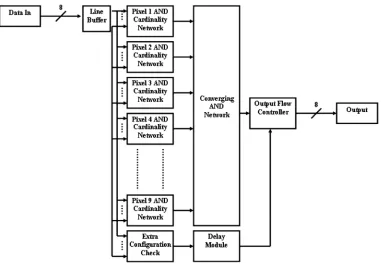
Figure6 shows the gate level designs for the binary soft closing system. The RTL level is again similar to Fig.1, apart from the two operation blocks now opening and closing and the data validator being the same. The gate level system is based around the basic SMO designs where the data input feeds the line buffers in order to create the3×3image seg-ment of the image set that will be processed. A series of AND gates with a constant value of “1” going into one input was used to detect the cardinality of the pixel configu-ration. However, instead of just using pixel 5 (the center pixel) and those surrounding it, all the pixel situations men-tioned will behave in the same way. All the pixels are added together and then subsequently added to the value of the pixel that is currently being taken as the center. This is because every pixel in turn acts as the center pixel for one situation. This is multiplied by the k-value before being added to the cardinality value from the other pixels, and before being compared to the k-value using a standard comparator. Either a“1”or “0”answer is produced for all nine pixels in the image segment; these are then ANDed together and passed through a second comparator whose threshold is set to a constant“9”and if the sum of all pixels is greater than this, then the output is a “1”and this is the final system answer to be output.
The circuitry converges from all the separate pixel groups with pixel 1 at the top and moving downward to pixel 9. At the bottom of the gate level design is the extra configuration check which is composed of four large four-inputANDgates. These gates stand to additionally safeguard against the incor-rect answer situations. Each input to these 4-inputANDgates
is inverted in order to find out when the pixel considered is a
“0.”If this condition is met then the output will be a“1”and so this is again inverted back to a“0.”This is then fed into a four-inputORgate, basic logic gates like two-inputORgates with both inputs tied together act as delays (the delay module block in Fig.6) to keep the signal in synchronization with the data passing through the other parts of the system. A product block is placed between the output from the other part of the circuit and the output port so that if the pixels are not all zeros; a “1” would be passed from the output of one of theANDgates through theORgate and delays into the product, thus allowing the system to output the data. If they are all
“0”s then a “0” is passed to the product and no data is allowed to leave the block. This condition is represented by the output flow controller block in Fig.6.
3.6 Grayscale Soft Opening Circuitry
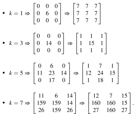
Showing all the steps with all the calculations for even a small k-value of 7 would again take several pages and so the highlights of just one example case,
0
@f∘ SE¼
$ 12 7 24
216 180 15 27 160 18
%
°
2
411 11 11 1 1 1
3 5
1 A;
are shown; the intermediate steps SE have also been omitted again for the same reason. The first matrix represents the intermediate value while the second matrix represents the final image set:
[image:8.630.348.543.350.388.2] [image:8.630.126.508.471.737.2]• k¼1⇒
2
400 06 00 0 0 0
3 5⇒
2
477 77 77 7 7 7
3 5
• k¼3⇒
2
400 140 00 0 0 0
3 5⇒
2
411 151 11 1 1 1
3 5
• k¼5⇒
2
4110 236 140 0 17 0
3 5⇒
2
4121 247 151 1 18 1
3 5
• k¼7⇒
2
415911 1596 1414 26 159 26
3 5⇒
2
416012 1607 1515 27 160 27
3 5:
From this work, a clear pattern began to form: after culating the initial stage, this rule can then be applied to cal-culate the final values which can be easily modified for the SE4 and therefore has not been shown:
• Fork¼1: all pixels become the intermediate pixel and add one.
• Fork¼2→7: add one to all pixels in the intermediate result.
The process is very similar to the binary operations thus showing how similar techniques can be applied to higher dimensional imagery. Again, this can be represented math-ematically by:
f∘½β;α; k ¼ ðf⊖½β;α; kÞ ½β;α; k
¼minkfk⋄½fðz1Þ−αxðz1Þ∪f½z2−βxðz2Þg þ1: (15)
This means that the circuitry to perform grayscale soft opening is the same as the grayscale soft erosion circuit, but with a “1” added to the result before the data is output.
3.7 Grayscale Soft Closing Circuitry Here is a single case for grayscale closing:
0
@f·SE¼
2
4211199 2731 3134 201 32 30
3 5·
2
411 11 11 1 1 1
3 5
1 A;
but as can be seen from the data there is no direct pattern. Therefore, the intermediate value of each pixel had to be cal-culated from the surrounding pixels, then the basic SMO method is used to calculate the final value. This is almost a cascaded operation, but as it uses the values directly with-out any intermediate memory storage used, it is“technically” classed as a direct implementation method.
• k¼1⇒
2
4212212 212212 3535 202 202 25
3 5⇒
2
400 340 00 0 0 0
3 5
• k¼3⇒
2
4212200 20035 3235 202 33 32
3 5⇒
2
400 320 00 0 0 0
3 5
[image:9.630.71.294.66.256.2]• k¼5⇒
2
4212200 3233 3235 202 33 31
3 5⇒
2
4320 3132 310 0 32 0
3 5
• k¼7⇒
2
4218200 2832 3235 202 33 31
3 5⇒
2 6 6 6
31 27 31 199 31 31 32 32 30
3 7 7 7.
Figure7shows the RTL level design for grayscale clos-ing. The gate level blocks are very similar to the system used previously as in Fig.4, where the bus comparators compare the signals for both highest and lowest values. In this case, the highest finds the answer for that particulark-value, while the lowest preserves the nonhighest values so that they can be used in the next block to find the next highest value. However, here a similar process is done as with the soft binary closing case where each pixel in turn acts as the center pixel, so each block outputs the nine highest pixel values for each of the nine pixel cases, while passing the unused data along with copies of the core(s) to the next block for the process to be repeated six times, in order to produce the seven k-value possibilities. These nine pixel values for each of the seven blocks are sent to the dilation decision maker block. This block works in a similar manner to the output decision block described previously.
In this final output block, all inputs are connected to prod-uct blocks which are also connected to a basic comparator block where the pixels of each block have a constant value of “1” fed into one of the inputs of the comparator only when the other input has thek-value going into the sys-tem. This comparator output is connected to the product block and is repeated for all possible combinations of pixels. For example, ifk¼1then the pixels from 1 to 9 for that case
will be allowed to continue to progress through the system, whereas all others will be turned into“0”s. Every like pixel is connected into the same OR gate network so that all pixels numbered 1 are connected together; all pixels numbered 2 are connected together, etc. Since only one will be active at any one time, the value will remain unaffected reaching the output of the network which is connected to the output port for that particular pixel. This ensures that the correct values are sent out to the next stage, which is the soft gray-scale erosion block that performs the second stage in the closing process and is then output as the answer.
4 Simulation Results, Size Comparisons, and Resource Allocations
Figure8(a)–8(d)shows the results for the binary tests. All these tests were conducted with a 640×480 color image that was converted to binary when sent into the DSP Builder simulation. The outputs from these systems were as in a previous work1 and ran through a MATLAB m-file code to compare the number of pixels and locations to a check image for validity. This check image was produced using the MATLAB image processing toolbox as a starting point and then incorporating the equations shown earlier that govern the morphology to calculate the check images in order to get the higher k-values. These were calculated using the same sweeping pattern over the image that the DSP Builder simulation would use and was originally tested on smaller images of which could be calculated by hand to provide additional validity. Some of these hand calculations are shown in a cut-down capacity due to their length in Sec.3 when the development of systems was discussed and the entire calculations can be found in Ref.17.
The results show that the DSP Builder systems and MATLABchecks that thek¼1systems are identical [Fig.8(b)
Fig. 8 Simulation results for binary operations, (a) Binary counterpart of original image. (b) Morphological dilationk¼1result, (c)MATLABdilation
[image:10.630.75.278.62.150.2] [image:10.630.137.488.457.725.2]and8(c)locations are identical] with all changes occurring in the same places. For the k¼7 case, the two situations are very similar. This occurs in both binary and grayscale situa-tions and is best described by looking at it from a ranked point of view. Dilation will be the highest. As the k-value increases it moves down the “ladder” of ranked values to lower values, whereas the erosion always stays at the same level on the “ladder” because a new copy of the core is always added with each k-value and so the lowest, second lowest, etc, always take place on the ninth highest“ladder” level. This is visualized below. The higher the k-value, the nearer the erosion and dilation output images will move towards each other. This will be more noticeable in binary images because there are only two possible data values, while with the grayscale system you can also tell a distinct difference between thek¼1andk¼7values, and how the similarity of the images become clearer.
• First ladder level¼dilation wherek¼1
• Second ladder level¼dilation wherek¼2
• Third ladder level¼dilation wherek¼3
• Fourth ladderlevel¼dilationwhere k¼4
• Fifth ladder level¼dilation wherek¼5
• Sixth ladderlevel¼dilationwhere k¼6
• Seventh ladderlevel¼dilationwhere k¼7
• Eighth ladder level¼unused
• Ninth ladder level¼erosionwherek¼1→7
• Tenth ladder level¼unused.
However, during testing there was a problem encountered with the binary erosion and so a bias value of“2”had to be added onto the existingk-value. This was because originally the output image set was saturated with zeros and upon examination of the output, it was discovered that the values in the output data stream ranged from“1”to“9”before the comparator. Therefore, if thek-value is“1”or greater then the output image will simply saturate. Different comparator settings were implemented, including having no comparator before adding a bias signal into thek-value. This was deter-mined through a trial and error process until the output from the DSP Builder model matched theMATLABtest comparison images to help eliminate design errors within the DSP Builder GUIC.
For size comparisons, the binary SMO system is virtually identical (especially the dilation system) to the binary MO system1 with the only difference being the comparator block used to compare the value obtained from the LHS of Eq. (4) to thek-value. The erosion circuit is slightly larger due to the circuitry required to calculate the value obtained from the RHS of Eq. (3) for the comparison stage of the system. Again, complexity is very similar to the standard systems, and so the soft system is better since it can do everything the standard system can and more, at the cost of an equivalent or slightly larger size. For the grayscale system, however, in either case if the separated-k or multi-ksystem is used, the size is approximately eight times larger for the SMO system than the MO system.1This is pri-marily due to the fact that there is a block similar in size to the original system for eachk-value. There is then a decision block required due to there being no other feasible way in
order to reduce the size of this any further. However, all the original functionality of the system is retained and the benefit of noise immunity is the advantage that should out-weigh the slight increase in size.
For the advanced operations, the results show that the DSP Builder systems andMATLABchecks for thek¼1 sys-tems are identical, with all of the changes occurring in all the same places as in the previous tests. There are differences and similarities between the images within the grayscale dimension. The differences in the image were far easier to spot and the user could tell a marked change in the pixel intensities for each individual operation, especially when using the “imagesc”command in the MATLAB environment rather than the“imshow”command.
The similarities were that the holes in each of the images were in the same place as in the basic operations. The differences are that some holes were eliminated and appeared to have been smoothed, and small areas like the edge change on the chest of the cat were fused together. These are all clas-sic signs of closing and thus proving the system works as expected. When thek-value is increased tok¼7for exam-ple, the opening operation output image had completely satu-rated. Investigation calculations were performed and the right-hand side of the equation for erosion≥k:Card½B1þ
Card½B2−kþ1 always gives either“5”for the SE4 case
or “9” for the SE8 case, since the core of the SE is only one pixel and this is counteracted by the −k term in the equation. Also, as thek-value increases the maximum pos-sible value on the left-hand side of the equationðk:Card½A∩
ðB1Þx þCard½A∩ðB2ÞxÞ becomes gradually greater until
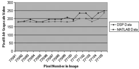
when k¼7, where it can reach a value of “11” for the SE4 case and “15” for the SE8 case, which is far above the values of“5”and “9,” respectively, thus the image set has a far greater chance of saturating at higher k-value s. The SE4 case gave more highly depleted output images because of the fewer number of active pixels inside the SE. Figure9and Table1show the details of the comparison process that took place to confirm that the DSP Builder out-put file matches the MATLABcheck image produced by the Image Processing Toolbox inspired m-file. Figure9 shows the strings of pixel values produced by the“reshape” com-mand inMATLAB. This command takes data from a matrix (i.e., the image) and presents it as a data string that can be plotted. From this graph it can be seen that the two sets of pixel values are virtually identical and follow the same trends and slopes to within a slight variation. This variation is caused by the fact that theMATLAB system has more processing power, can implement loops within the
[image:11.630.323.566.605.726.2]system more easily than the DSP Builder system (hence why they are avoided if possible) and can handle boundary con-ditions differently by simply not considering the number out-side of the image set, in DSP Builder this was assumed to be
“0.”They are also very similar as MATLABhas been used to verify all the results in every stage in the development proc-ess from standard to soft morphology and this has obviously led to a trend that the DSP Builder systems developed follow the same trends as theMATLABchecks do. In order to explore this variation in a little more detail, another DSP Builder sys-tem was designed to compare the images and produce result-ant values to indicate how similar or dissimilar the images were. The system inputs the two images simultaneously via the eight-bit-wide input lines and diverts the signals into a series of blocks that look for either an exact match or a percentage match. The blocks themselves, if not looking
[image:12.630.62.304.83.236.2]for an exact match, input the DSP Builder image data into adder and subtractor blocks and either add or subtract a con-stant value to the pixel data in order to give the percentage variation. The constant value ranged from 13 pixels (the number of pixels needed to change between to the two images to give the follow percentage match) for a 95% match to64 pixels for a 75% match. These are then fed into comparators where an AND gate is used to combine the signals so that if both are in the desired range then the output logic“1”from theANDis used to enable a counter. This counter is then divided by the total number of pixels in the image and multiplied by 100 in order to give us a per-centage match which is output to theMATLABenvironment for checking. As shown in Table 1, this produced some very accurate matches in some cases, and most interesting of all, was how the binary accuracies were in fact lower than the grayscale which was the opposite to what was expected. Upon investigation, this was found to be produced by a slight phase shift incurred when the data is passed through the line buffer convolution kernel in order to produce the3×3image segment analyzed on each clock cycle and depending on how many are used, can cause a shift of between four and seven pixels in both the binary and grayscale imagery. This is another reason for reducing the number of line buffers in the system and so it not only helps to save resources on the FPGA board, but also allows for more accurate imaging. For size comparisons, the binary SMO systems are very similar or better than the binary MO system,1with the open-ing approximately 1.25 times the size of the original system. This is due to the gates which calculate the cardinality and comparisons for one of the pixel states in the SMO system being similar to one of the comparison stages which made up the MO system. The binary SMO closing system was very good being approximately 0.125 times the size of the binary
Table 1 Image comparison tolerances summary.
Match
Binary Basic
Binary Advanced
Greyscale Basic
Greyscale Advanced
100 75 69 77 70
95 −N∕A− −N∕A− 79 72
90 −N∕A− −N∕A− 89 72
85 −N∕A− −N∕A− 93 74
80 −N∕A− −N∕A− 96 79 75 −N∕A− −N∕A− 95 91
[image:12.630.144.490.451.723.2]MO system (this being similar to one of the comparison sys-tems) and the MO system used 8 to calculate closing. Since the opening operation is so similar to the basic operation for the grayscale systems, this is again eight times larger. Due to the number of calculations that are performed to develop an
“intermediate” result for the closing operation, which is directly fed into a copy of the erosion system, this system is approximately 72 times larger than the MO grayscale clos-ing, which unfortunately is a major drawback.
These sizes were obtained by doing a basic component/ gate count and comparison between the MO and SMO sys-tems. Of course, like with the basic operations, all the func-tionality of the MO systems was retained within the SMO systems.
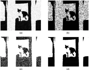
Various types of noise were added into the image in the form of Gaussian white noise with a constant mean and vari-ance, Poisson noise from the data instead of adding artificial noise to the data, and lastly“salt and pepper”noise. All of the latter was achieved using the built in functions ofMATLABand adding the noise as the data was sent into the DSP Builder simulation via the m-file to simulate as if the noise was cap-tured by a camera. This was accomplished by adding the
“imnoise” command in MATLAB into the m-file that sends the data in and out of the DSP Builder simulation environ-ment. When the images were run through the same SMO circuitry, the system produced similar results to the same margin of error as were obtained without the noise. This shows that the noise was eliminated from the white (binary
“0”) segments of the image in opening, and for closing, noise was eliminated from the black (binary“1”) segments of the image. This is shown in Fig.10(a)–10(c). When the two sep-arate images are combined, this completely removes all the noise in the image as in Fig.10(d).
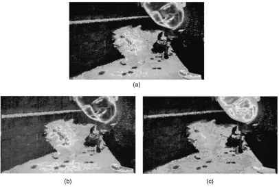
In order to provide completeness of the coverage of these simulations, Fig. 11 shows the results from the grayscale basic MOs system simulations. Shown in Fig.11(a) is the grayscale counterpart of the original image whilst Fig.11(b) and 11(c) show the dilation and erosion operations, respectively. As observed, there are changes between the original image and the two resultant steps, the main changes are that the dilation step causes the wall in Fig. 11(b) to become paler whilst the face and other features remain sim-ilar, however, the erosion step in Fig.11(c)causes the oppo-site, here the face is paler and the wall and remains the same. In all these simulations thek-value was set to“7”to focus on cases where k >7 to demonstrate this capability. These checks proved to provide valid results and the resultant imagery is similar to that shown in Fig.11(b) and11(c).
In embedded system design, there is a lot of flexibility in deciding which parts of the system should be embedded in the FPGA and which parts should remain as separate ICs. Possibly the most compelling choice is to integrate most of the system into the FPGA chip, including the processor and its peripherals (e.g., bus interfaces, parallel/serial and some of the memory, such as processor cache memory). One of the more vital aspects of the design is in performing Quartus II compilations on the produced VHDL code in order to gain an idea of how much resources these operators would use up when downloaded to a specific Altera device as these operators are designed to become part of a much larger image system which would require a capture device such as a camera which is outside the scope of this material (and hence why a complete computation time for a complete system can-not be included here). The device was changed in Quartus for the compilations by going to the Assignments>Device
[image:13.630.112.518.455.728.2]menu and selecting the appropriate board family. The results of these compilations are summarized in Table 2 for four
common board types: the APEX family using the 20K200EFC series board, the Cyclone II family using the EP2C35 series board, the Stratix I family using the EP1S25 series board, and finally the Stratix II family using the EP2S60 series board. These specifications are without the supporting NIOS processor to assist in the run-ning and real time operation of the system. The APEX board has 8320 logic elements (LE) and 376 pins, the Cyclone II has 33,216 LE and 322 pins, the Stratix I has 25,600 LE and 474 pins, and the Stratix II has 48,352 LE and 355 pins. The latter figures are shown in Table2, thus the LE usage is the un-bracketed percentage whilst the bracketed number is the pin usage. The pin usage stays the same as the same number of inputs and outputs are used on all the simulations but of course, these remaining pins are vital for when the operators are incorporated into a much larger system. Memory is not included here as each system only used eight memory delays
[image:14.630.63.567.80.227.2]in order to create the SE convolution kernel and the block type was set to automatic so that it selects the type of memory most practical for implementation from the M4K block memory or M512 block memory used on many of the Cyclone or Stratix series devices so this could differ when the operations are used in a real system. The failures are attributed to the system requiring more LE than there was available on the device and due to the large size for the direct implementation of the grayscale closing operation as no sim-ple direct method could be found. Under these situations it would be a more efficient use of resources to cascade the basic operations together rather than use the direct imple-mentation methodology as the slight increase in memory delays required would allow for an effective implementation of the advanced operations in this case. The binary direct operations are more resource efficient than the standard oper-ations and so this is the better implementation choice. Once
Table 2 Resource allocations for various Altera board families showing the percentage of logic elements (LE) and pins used.
Operation Description APEX Family Cyclone II Family Stratix I Family Stratix II Family
Binary Dilate/Erode 7%(2%) 1%(2%) 2%(1%) 1%(2%)
Greyscale Dilate/Erode Fail (2%) 8%(2%) 8%(1%) 8%(2%)
Binary Open 9%(2%) 1%(2%) 1%(1%) 1%(2%)
Binary Close >1%ð2%Þ >1%ð2%Þ >1%ð1%Þ >1%ð2%Þ
Greyscale Open Fail (2%) 24(2%) 48%(1%) 24%(2%) Greyscale Close Fail (2%) Fail (2%) Fail (1%) Fail (2%)
[image:14.630.69.554.455.738.2]again, all these trade-offs would have to be based on the end application of the system but either would be appropriate for a dedicated hardware system that could be used as part of another system. This means that the most suitable FPGA to successfully run these types of operations on would be a Stratix II family device or later as this used the least amount of resources.
The last issue to be discussed is the computation time. Figure12shows a matlab plot of the Simulink computation time for the simulation stage against the image size. The sizes of the images considered were 320×240,
640×480, 1000×1000, and 2000×2000, for an image of size 4000×4000, extra memory would need to be used in the system and so was not included. For the smaller images, the simulation time between the binary and gray-scale systems are fairly similar but when the image size increases over 640×480, this is where the two systems begin to diverge and logically, the grayscale system has a larger computation time to handle the eight-bit grayscale data in the images. The interesting point noticed was that the higher k-value morphological processes had a quicker processing time. It was discovered that this is due to the fact that in the decision making blocks and convergence net-works allow the k¼7 data to have a shorter propagation path than for k¼1 thus allowing for a quicker simulation time and system throughput.
5 Conclusions and Future Work
This paper has presented and examined a range of SMO structures for both binary and grayscale images for basic SEs. Extensive simulation results have shown that the proposed structures have improved performance over the MATLABinstructions provided by the image processing tool-box that provided the baseline for the comparison and debug-ging of this work. For higherk-values, a customMATLAB m-file was written to help provide the images for comparison purposes as the standard commands that come with the tool-box were not able to do this. The SMO operations developed here are using similar or slightly larger and more compli-cated circuitry than their MO counterparts. It is easy to inter-change image size by altering the image buffer delays and adding more buffers, along with some minor changes to the rewiring and a few constant values, allowing for a more complicated SE to be used if desired, whilst only affecting the gate level of the system. During an in-depth analysis, the system performs the same function to within the same margin of error, given that the image has been either corrupted with noise or not. This was tested several times using various types and combinations of noise and all the results provided the same verification.
The major disadvantages are that no direct implementa-tion pattern could be found for the grayscale closing, result-ing in the large increase in size of the system thus makresult-ing it undesirable to implement on an actual FPGA due to the inef-ficient use of device resources. Despite this, the advantages are that these systems have increased in size without an asso-ciated propagation delay problem that seems to have plagued previous versions of the system. These systems did not suffer as much from this problem primarily thanks to the dummy modules and delays used in their construction.
Future work will consist of developing more applica-tion specific systems for various tasks using this graphical
block methodology for robotic-based security systems such as those already developed and undergoing devel-opment,8,10,18,19 but specifically making them work on FPGA systems and with a feasibility study particularly focusing on morphology for the image processing and con-trol of robotic stereo vision systems, as well as continuing the work on implementation strategies and more detailed FPGA resource usages for these developed circuits. Implementation work will continue from the work already completed on basic SISO and SIMO systems comprising all of the res-pective levels of abstraction to obtain a practical use of the DSP Builder system for the FPGA. This work will then be combined with other work on the use of a system-on-a-programmablechip camera system, controllers of ser-vos and stepper motors, and the development of a wireless communication system, all for implementation on an FPGA so that practical real-world applications can be become a reality.
Acknowledgments
The authors would like to thank the associate editor and anonymous reviewers for their valuable comments and suggestions. Andrew Tickle would also like to thank the Engineering and Physical Science Research Council (EPSRC) for funding this research work during his PhD. Paul Harvey would also like to thank the UK Student Recruitment Office Scholarship (UKSRO) for funding his contributions during his MSc(Eng) and to Altera for their technical support.
References
1. A. J. Tickle, J. S. Smith, and Q. H. Wu,“Development of morphological operators for field programmable gate arrays,”IOP Electron. J. Phys. Conf. Ser.76(1), 012028 (2007).
2. A. J. Tickle, J. S. Smith, and Q. H. Wu,“Feasibility of a multifunctional morphological system for use on field programmable gate arrays,”
IOP Electron. J. Phys. Conf. Ser.76(1), 012055 (2007).
3. L. Koskinen, J. Astola, and Y. Neuvo,“Soft morphological filters,”
Proc. SPIE1568, 262–270 (1991).
4. J. Poikonen and A. Paasio,“A ranked order filter implementation for parallel analog processing,”IEEE Trans. Circ. Syst.51(5), 974–987 (2004).
5. C. M. Higgins and V. Pant, “A biomimetic VLSI sensor for visual tracking of small moving targets,” IEEE Trans. Circ. Syst. 51(12), 2384–2394 (2004).
6. A. J. Tickle et al.,“Image processing virtual circuitry for physics based applications on field programmable gate arrays,” Proc. SPIE7100, 71002I (2008).
7. T. Good and M. Benaissa, “Very small FPGA application-specific instruction processor for AES,” IEEE Trans. Circ. Syst. 53(7), 1477–1486 (2006).
8. A. J. Tickle et al.,“Feasibility of an encryption and decryption system for messages and images using a field programmable gate array as the portable encryption key platform,”Proc. SPIE7100, 71002N (2008). 9. L. Yang, H. Liu, and C. J. R. Shi,“Code construction and FPGA imple-mentation of a low-error-floor multi-rate low-density Parity-check code decoder,”IEEE Trans. Circ. Syst.53(4), 892–904 (2006).
10. A. J. Tickle, J. S. Smith, and Q. H. Wu,“Feasibility of a portable mor-phological scene change detection security system for field program-mable gate arrays (FPGA),”Proc. SPIE6978, 69780V (2008). 11. P. Kuosmanen and J. Astola,“Soft morphological filtering,”J. Math.
Imag. Vision5(3), 231–262 (1995).
12. P. Dudek and P. J. Hicks,“A general purpose processor-per-pixel analog SIMD vision chip,”IEEE Trans. Circ. Syst.52(1), 13–20 (2005). 13. T. Y. W. Choi, B. E. Shi, and K. A. Boahen,“An ON-OFF orientation
selective address event representation image transceiver chip,”
IEEE Trans. Circ. Syst.51(2), 342–353 (2004).
14. E. Aho et al.,“Block-level parallel processing for scaling evenly divis-ible images,”IEEE Trans. Circ. Syst.52(12), 2717–2725 (2005). 15. C. C. Pu and F. Y. Shih,“Threshold decomposition of grey-scale soft
16. R. B. Fisher,“CVonline: the evolving, distributed, nproprietary, on-line compendium of computer vision,”http://homepages.inf.ed.ac.uk/ rbf/CVonline/(November 2007).
17. A. J. Tickle,“Applications of morphological operators on field pro-grammable gate arrays,” Doctoral Thesis, Univ. of Liverpool, pp. 326–332 (2009).
18. A. J. Tickle, J. S. Smith, and Q. H. Wu,“A grayscale skin and facial detection mechanism for use in conjunction with security system tech-nology via graphical block methodologies for on field programmable gate arrays,”Proc. SPIE6978, 69780Q (2008).
19. A. J. Tickle, P. K. Harvey, and J. S. Smith,“Applications of a morpho-logical scene change detector (MSCD) for visual leak and failure iden-tification in process and chemical engineering,” Proc. SPIE 7833, 78330W (2010).
Andrew J. Ticklereceived an ME (Hons) degree in electrical engineering and electron-ics from the University of Liverpool, UK in 2005 and was ranked fourth in his year. He obtained a PhD degree in the field of com-puter electronics and robotics from the same university in 2009. His research inter-ests include embedded system development, digital signal processing, security manage-ment technologies, autonomous mobile robots, and electronics for astrophysical applications. He worked as an Engineering and Physical Sciences Research Council (EPSRC) PhD, and also as a research fellow from 2009 to 2010 whilst serving as a university teacher at Liverpool from 2009 to 2011. He is currently a lecturer of electrical/ electronic engineering at Coventry University and a nonexecutive director of Crosby Communications PLC and Crosby Systems Limited. He is a chartered engineer, chartered physicist, and is cur-rently a member of the IET, IEEE, IOP, and SPIE, serving on several conference and technical committee panels.
Paul K. Harvey graduated from the University of Liverpool in 2005 with a BE (Hons) degree in electrical engineering and electronics before completing a certificate in welding and fabrication in 2006. He later returned to the university in 2007 for his MSc (Eng) in telecommunications and micro-electronic systems. His research interests include complex plasma systems, embedded system design and simulation, and computer communication systems. He is currently working as a freelance engineering consultant.
Jeremy S. Smith graduated from the University of Liverpool and was awarded his PhD in 1990. Since then he has taken teaching positions as lecturer, senior lecture, reader, and professor at the same university. From 2006 to 2010, he was the academic dean and later the vice-president of Xi’an Jiaotong Liverpool University. His academic research interests are development of vision-based sensors and control systems to be used in advanced robotic systems for automated welding and other manufacturing processes, development of advanced digital systems based upon system-on-a-programmable chip devices and parallel processing systems, development of neural network and fuzzy logic techniques to allow the fusion of data from a number of sensors to provide control information. Other areas of research include the development of a networking system based upon the CAN bus, the development of robotic manipulator control-lers, and the development of an advanced remotely operated under-water vehicle (ROV) requiring the integration of vision and manipulator systems along with sophisticated navigation techniques.