This is a repository copy of Diffusion-Controlled Faradaic Charge Storage in High-Performance Solid Electrolyte-Gated Zinc Oxide Thin-Film Transistors. White Rose Research Online URL for this paper:
http://eprints.whiterose.ac.uk/129109/ Version: Accepted Version
Article:
Balakrishna Pillai, P. orcid.org/0000-0001-7272-9923, Kumar, A., Song, X. et al. (1 more author) (2018) Diffusion-Controlled Faradaic Charge Storage in High-Performance Solid Electrolyte-Gated Zinc Oxide Thin-Film Transistors. ACS Applied Materials and Interfaces, 10 (11). pp. 9782-9791. ISSN 1944-8244
https://doi.org/10.1021/acsami.7b14768
Reuse
Items deposited in White Rose Research Online are protected by copyright, with all rights reserved unless indicated otherwise. They may be downloaded and/or printed for private study, or other acts as permitted by national copyright laws. The publisher or other rights holders may allow further reproduction and re-use of the full text version. This is indicated by the licence information on the White Rose Research Online record for the item.
Takedown
If you consider content in White Rose Research Online to be in breach of UK law, please notify us by
Diffusion controlled Faradaic charge storage in high
performance solid electrolyte gated Zinc Oxide thin
film transistors
Premlal Balakrishna. Pillai, Ashwani Kumar, Xiaoyao Song, Maria Merlyne De Souza*
Department of Electronic and Electrical Engineering, University of Sheffield- North campus, S3 7HQ, Sheffield, UK
KEYWORDS : ionic diffusion, tantalum oxide, oxygen vacancies, synaptic memory, thin film transistors
108-109. The non-volatile behaviour of the interface charge storage and slow diffusion of ions is utilized in efficiently emulating Spike Timing Dependent Plasticity at similar time scales of biological synapses and unveils the possibility of STDP behaviour using multiple in plane gates that alleviate additional requirement of waveform shaping circuits
1. INTRODUCTION
charge storage (Faradaic type) mechanism is revealed in solid electrolyte based two terminal resistive switching devices.30,31 The charge storage mechanism in super capacitor based and battery type electrochemical storage devices has been a subject of intense research32,33 where supercapacitors are categorized as electrochemical double layer capacitors (EDLCs) and pseudo capacitors owing to their difference in the storage mechanism. EDLCs utilise reversible adsorption of ions of the liquid/solid electrolyte onto electrochemically stable electrode materials that have a high specific surface area.34 The double layer capacitance is given as
(1)
where is the relative permittivity of the electrolyte, is the dielectric constant of free space, d is the effective thickness of the double layer (charge separation distance) and A is the electrode surface area. In a typical EDLC, the separation d is of the order of the radius of the solvated ions.35,36 Pseudo capacitance, on the other hand, is given as
(2)
Despite the fact that there are multiple charge storage mechanisms possible at the metal/insulating oxide/semiconductor layers, majority of the TCO based liquid/solid electrolyte devices reported to date, have been identified as electric double layers FETs.21,25,40,41 We have recently demonstrated a solid electrolyte based three terminal Zinc oxide synaptic device featuring a gate polarity induced drift motion and accumulation of mobile vacancies in the Ta2O5 gate insulator, with an effective modulation of channel conductance depending on the density of accumulated positive charge at the channel interface.42 The present study elucidates a diffusion controlled charge storage mechanism employing oxygen ions/vacancies in the high k gate insulator using cyclic voltammetry (CV) and chronoamperometry and presents new opportunities for realising high performance thin film display and synaptic memory devices with a distinctly different charge storage mechanism from conventional EDL based thin film devices. The electrochemical charge storage mechanism in the gate insulator/semiconductor layers presents a pronounced enhancement in the induced carrier density in the semiconducting channel that leads to superior transconductance and memory retention.
2. EXPERIMENTAL METHODS
Bottom gated three-terminal thin-film transistors in this study composed of a conducting Indium Tin Oxide (ITO, 20 /square) layer as gate, a high k dielectric tantalum oxide (Ta2O5) of
dielectric constant is deposited as the gate insulator and a of zinc oxide is
semiconductor device parameter analyzer/Semiconductor characterization System interfaced with a Desert Cryogenic probe station. Measurements of Spike Timing Dependent Plasticity are performed with the help of a RIGOL 4162 arbitrary wave form generator and the B1500A Semiconductor Characterization System, where the wave forms are designed using a Keysight Bench link Waveform builder (33503A). All the electrical measurements reported in this work are carried out at room temperature at ambient atmosphere.
3. RESULTS AND DISCUSSION
Despite the fact that cyclic voltammetry is conventionally applied to three electrode systems with a working, reference and counter electrode geometry, it is proven as a suitable technique to study various solid electrochemical cells such as Pt/Ta2O5/Pt, Pt/HfO2/Pt or Pt/Ta2O5/Ta where the host ions such as oxygen and/or metal ions can be transported.44. In the present study, a solid electrolyte material (Ta2O5) is sandwiched between a metal/semiconductor layer and bottom ITO layer where the leakage current is minimized by optimizing the thickness of the insulating Ta2O5 layer, enabling the observation of ionic features (oxidation/reduction) in a two terminal geometry. In general, cyclic voltammetry is widely employed to understand the electrochemical diffusion of metal cations in oxides.31
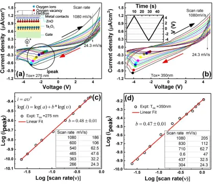
shows the accumulation of positive ionic charge towards the channel interface, due to an applied positive gate bias. A representative triangular waveform at a fixed ramp rate used for the CV sweep is shown in the inset of Figure 1b where the voltage sweep is performed from
. The oxidation (positive) and reduction (negative) current reveals a strong scan rate dependence, as highlighted in the figures, where the position of the reduction peak arising from a recombination of positively charged oxygen vacancies with negatively charged oxygen ions. As the electric field for the oxidization reaction is reduced in the backward sweep, the corresponding current also drops and the reduction process of the positive ions starts at where the current becomes negative. Sweeping the voltage to more negative values results in the reduction current attaining a peak value . The scan rate dependence of the
peak current for the 275 and 350 nm gate insulator devices are shown in Figure 1c, d respectively. The figures depict a power law relationship of between and scan
(3)
where n is the electron number involved in the electrode reaction, F is the Faraday constant= 96,500 C/mol, A is the surface area of the electrode material, C is the surface concentration of
the intercalated cation, is the transfer coefficient, R is the molar gas constant=8.3144 in J K
-1mol-1, D is the diffusion coefficient in cm2/s, T is the absolute temperature, (bt) is the
normalized current for a totally irreversible system in CV. This behaviour is fundamentally different from a capacitance dominated process valid in the case of EDLC and pseudocapacitances, where the current and scan rate relationship is34
Figure 1. Cyclic voltammetry (CV) data revealing electrochemical kinetics of the ZnO devices
measured in the Gate /Insulator /Semiconductor /Metal geometry. I-V characteristics are
acquired at different scan rates for a) 275 nm and b) 350nm Ta2O5 gate insulator ZnO TFT with
W/L of 200/2.5 µm. The area of the device is which is considered as the area
of overlap between the top and bottom electrodes. A positive gate voltage leads to the
accumulation of positive charge from the insulator at the semiconductor interface that induces
corresponding image charge (electrons) in the n-type ZnO semiconductor as shown in the inset
of (a). The reduction peak highlighted in (a) and (b) corresponds to a recombination of the
symmetric triangular waveform is used for the CV sweep, shown in the inset of fig (b). Figures
(c) and (d) reveal a power law relationship between the peak current ( ) of the reduction
reaction and the scan rate ( , where ~ 0.5 implies that the current is mainly controlled by
solid state diffusion of the mobile ions in the gate insulator48. Comparing the data from 10
devices, the variations in peak values of gate current and reduction current from device to device
is up to 0.5, 0.3 nA respectively . Hence the error bars associated with the logarithmic value of
the reduction currents in (c) and (d) are smaller than the size of the symbol and omitted in the
data. Scan rates used in (a) and (b) are tabulated in the inset of (c) and (d) respectively.
where is the area-normalized capacitance. Cyclic voltammetry is a powerful technique for identifying the respective mechanisms, even in complicated scenarios where contributions from capacitive and diffusion controlled processes are present.38,49 Following equations (3) and (4), it
can be seen that the diffusion controlled peak current (in a battery) is proportional to
following a power law relationship of between and scan rate ( ) with
. On the other hand, a capacitance controlled current in a supercapacitor varies linearly with scan rate yielding b~1. It has been unambiguously shown that capacitance controlled processes,
including intercalation pseudocapacitance, are not diffusion controlled and exhibit “b” of ~1 38,50
, unlike the present case where a dependence of with is prevalent. A similar variation
of the reduction peak current is mainly observed for battery electrode materials such as LiFePO4 51, TiO2 mesocages52, Na3V2(PO4)3 53 and Li–S 54. These results support the idea that ZnO
Figure 2. a) Dependence of the diffusion coefficient of positively charged oxygen vacancies
with varying ion concentration at the channel interface revealing two distinct regions. Region 1 ( > 100 mV/s) corresponds to a fast charging regime, where shows a steep variation with ion concentration, while in region 2 (< 100 mV/s) it is nearly independent of b) Chronoamperometric data is acquired at three applied biases, where the transient behaviour of the charging current can be well described using the Cottrell equation36 applicable for diffusion controlled Faradaic (battery) devices. Figure inset shows a similar reduction in the value with increase in . The error bar represents uncertainty arising from device to device variations in the gate current.
cm2/s at moderate scan rates compares well with others reported in the literature55 (3.5 × 10⁻¹³ cm2/s. The calculated diffusion coefficient in Figure 2a shows distinct scan rate dependence corresponding to fast charging (region 1, scan rate >100 mV/s) and a weak dependence of scan rate or ion concentration in region 2, where the scan rate < 100 mV/s (slow charging). The observed behaviour can be attributed to enhanced screening between the ions when their concentration increases (high low scan rates)31, finally resulting in saturated diffusion of ions (scan rates <100 mV/s).
The observed battery behaviour in the Ta2O5/ZnO devices is further investigated using the Chronoamperometry technique where the voltage is stepped within the region where the current is limited by diffusion controlled process, and the current is measured as a function of time. The current decreases with time because the ion concentration gradient near the electrode decreases with time as56
where x is the position, t is the time, D is the diffusion coefficient and C is the bulk concentration of reacting species.
The diffusion current from the concentration gradient is obtained as56
(6)
Here is the formal electrode potential, D0 is the diffusion coefficient of oxidising species. If
the voltage is stepped into a diffusion limited region, then E>> and
(7)
Equation (7) is the general form of the Cottrell equation36 showing the transient response of current is inversely proportional to the square root of time, whereas charging current is a capacitance controlled system generally expressed as:
�xp (8)
The charge storage induced equivalent battery voltage in our device is further investigated in supporting info Figure S1a-c. It is understood that the generated electromotive force in the device due to polarization of charge scales with logarithmic ionic charge density as shown in
Figure S1c, following the Nernst equation, ln , where is the activity of an
ion, that is related to its concentration as , where is the activity coefficient (ideally 1) and is the ionic concentration.59 Having demonstrated the occurrence of battery controlled charge storage mechanism in Ta2O5/ZnO, the consequential effect of this interface charge storage on the performance of the thin film transistors and their suitability for demonstrating neuromorphic behavior are discussed below.
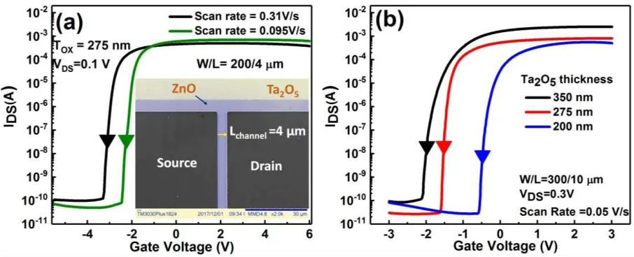
Figure 3: a) Scan rate dependence during the backward sweep (high to low) IDS-VGS characteristics of the 275 nm oxide device. (Figure inset shows the false colour SEM image of the device showing the gate insulator, ZnO mesa and Aluminium source/drain contacts, the scale bar is 30 µm) b) A comparison of backward sweep transfer characteristics of the ZnO FETs employing Ta2O5 insulator thickness of 200 nm, 275 nm and 350 nm. Device to device variations can result in up to 0.5 mA differences in the saturated on current values.
[image:15.612.84.537.72.256.2]behaviour of the mobile charge species in the insulator with that reported elsewhere for Ta2O5 based resistive switching devices.44,61
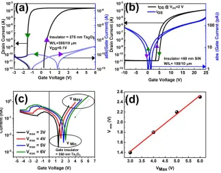
Figure 4. a) Transfer characteristics of two TFTs fabricated using a) using RF sputtered 275 nm
Ta2O5 showing a prominent counter clockwise hysteresis b) shows the characteristics of a TFT with 50 nm PECVD grown SiNx insulator, revealing a clock-wise hysteresis. c) Variation of the minimum of gate current characteristics in the device in the backward sweep when the starting voltage (Vmax) is changed from 3V to 6V for a TFT with 350 nm thickness of Ta2O5 insulator. d) Shows a linear relationship between the maximum applied voltage (Vmax) and the voltage (Vmin) corresponding to the minimum gate current in (c).
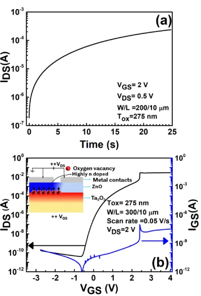
[image:16.612.153.476.136.389.2]Figure 5. a) A typical transient behavior of the drain current in the ZnO solid electrolyte FET at
[image:18.612.207.406.65.357.2]The performance metric of the ZnO based solid electrolyte TFTs in the study is considered below. From the CV data for the lowest scan rate shown in Figure 1, the induced interface electron density in ZnO corresponding to a peak gate voltage of 4.75 V is roughly estimated as
n Q � = 4.24 × 1014 cm-2. The specific capacitance corresponding to the above value is
[image:19.612.68.545.563.695.2]calculated as 14.3 µF/cm2 and is approximately 4 X higher than the specific capacitance reported in other solid electrolytes. 41,53,63,64 The induced electron density in a 40 nm ZnO channel due to the accumulated oxygen vacancies is calculated to be ~ 1.06 × 1020 cm-3 and this value is comparable to the electron density in heavily doped Al or Ti- ZnO.65,66 It can be understood that the high on-state conductance shown by these devices is primarily due to the reversible battery type charge storage of oxygen vacancies at the interface, resulting in an enhanced electron density in ZnO. The Ta2O5 based solid electrolyte devices shows greater promise compared to other technologies in terms of delivering a higher stable specific capacitance up to 15 µF/cm2 with no reduction at higher applied biases and the diffusion controlled mechanism in our devices delivers highest normalized transconductance compared to other solid EDLFETs reported in literature.41,53,64,67. The main performance parameters are summarized in Table 1, where a comparison with other ZnO based EDL FETs is also reported.
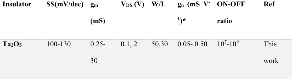
Table 1. Performance of EDL- FETs Vs Ta2O5/ZnO device.
Insulator SS(mV/dec) gm
(mS)
VDS (V) W/L gn (mS V
-1)*
ON-OFF
ratio
Ref
Ta2O5 100-130 0.25-
30
P(VDF-TrFE)a
- 0.0025 0.1 1.56 0.016 107 67
PSGb 100 0.36 1.5 12.5 0.02 >107 40
Chitosanc 65 0.2 1.2 12.5 0.01 107 41
KH550-GOd
140 0.8 2 12.5 0.03 3×10⁷ 64
ILse - 0.16 0.1 0.4 4.00 3-103 25
CSPEf 115 0.003 0.5 0.02 0.29 107 68
a (poly( -(1-4)-D-glucosamine), poly[(vinylidenefluoride-co-trifluoroethylene], bPhosphosilicate
glass, cChitosan, d 3-triethoxysilylpropyla-mine-graphene oxide, e N,N-diethyl-N-(2-methoxyethyl)-N-methylammonium bis- trifluoro-methylsulfonyl)-imide (DEME-TFSI), composite solid polymer electrolyte. *
dilemma’.71 A non- volatile redox transistor (NVRT) employing battery type materials such as
Li1-xCoO2 or Nafion electrolyte gated organic polymers as channel is proposed as a viable option to alleviate the high write voltage requirement and short term data retention limitations of the resistive switching devices for neuromorphic applications.11,72 Moreover, the three terminal configuration of these devices allows independent read operation across the source drain electrodes, while the write operation is via a potential on the gate terminal. The inherently slow diffusion of ions in these battery type materials significantly helps towards long term retention of channel conductivity in the absence of an applied gate voltage and owing to the low activation energy of mobile ions to transfer from the electrolyte to electrode materials results in low write voltages.11,72
The ZnO based solid electrolyte technology demonstrated here offers unique advantages over other reported devices owing to their improved stability arising from the inorganic structure and dramatically simpler device design. The interface Faradaic charge storage mechanism in these devices provides robust memory behaviour where the channel conductance can be maintained even after removing the gate stimuli. A more beneficial property of the solid electrolyte ZnO
synaptic device over other ‘battery like’ synaptic devices is the normally off behavior that is
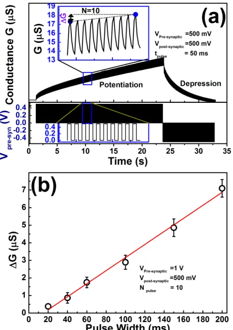
on change of synaptic weight (conductance) with potentiation evident with a pulse width as low as ~20 ms. The conductance change with these short ms pulses is associated with short term memory retention which lasts for only few seconds.
Figure 6.(a) synaptic potentiation and depression by the application of repetitive positive and
[image:22.612.187.427.166.506.2]device parameters are W/L = 300/10 µm and toxide=275 nm. The error bar represents typical device to device variations.
The limiting factor of the ionic FETs at lower pulse duration is the low mobility of oxygen vacancies/ions in the gate dielectric (~1 x 10-11 cm2/Vs). Improving the ion mobility in the oxide can significantly enhance the operation speed and reduce hysteresis at low frequency operation.
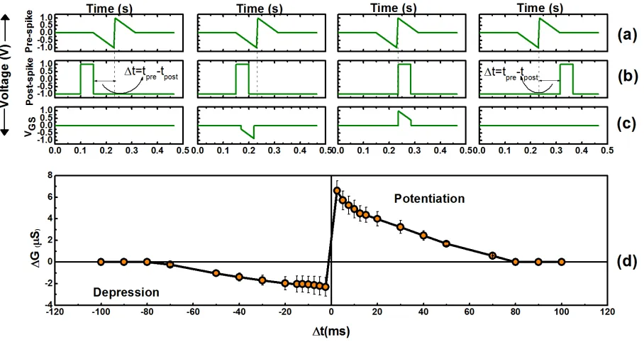
STDP behavior of synapses. The asymmetric STDP behaviour of a synapse73 is effectively emulated using the solid electrolyte ZnO TFTs as shown in Figure 7.
Figure 7. Demonstration of asymmetric spike timing dependent plasticity from a representative
ZnO synaptic FETs. a) a bipolar saw-edged wave form is selected as a pre-spike and a voltage pulse with width of 50 ms is used as the post-spike, with a pulse amplitude of 1V (b). The two wave forms are combined and the resultant wave form in (c) is fed to the gate terminal to emulate the asymmetric STDP behaviour shown in (d). The synaptic weight (conductance) is measured with a drain-source voltage of 200 mV. Device parameters are W/L = 200/4 µm, Tox = 275 nm, VDS=200 mV. The error bar in (d) represents typical device to device variation in the channel conductance.
revealed in the STDP measurements in hippocampal glutamatergic synapses by Bi and Poo 73, synaptic potentiation is demonstrated when the pre-spike precedes a post spike (
>0) and synaptic depression when the pre-neuron spikes after the post neuron signal (
). The post synaptic response across the source and drain terminals were measured using a drain voltage of 200 mV as shown in Figure 7d. The demonstrated STDP behaviour here can also be realized using two presynaptic gate terminals in the vicinity of the channel region, where respective pre-spike and post spike signals can be applied on these gate terminals. Hence using multiple gate architecture, coupled to the channel using a solid electrolyte insulator, STDP behaviour as shown in Figure 7d can be emulated using a single device, without the need of any wave shaping circuits or software based waveform mixing approaches.
4. CONCLUSION
while displaying synaptic behaviour with an induced EMF, is analogous to biological neurons with a fixed membrane potential and offer promise in realising future neuromorphic devices and circuits using fully transparent thin film technology. The solid electrolyte based technology demonstrated here is extendable to other material platforms for realising high performance memory devices that mimic biological synaptic functions.
▪ SUPPORTING INFORMATION
Additional characterization data regarding measurement of the battery voltage using CV data are presented.
▪ ACKNOWLEDGEMENT
We gratefully acknowledge funds from the ENIAC JU project E2SG under grant number 296131
REFERENCES
(1) Wen, Z.; Yeh, M.-H.; Guo, H.; Wang, J.; Zi, Y.; Xu, W.; Deng, J.; Zhu, L.; Wang, X.; Hu, C.; Zhu, L.; Sun, X.; Wang, Z. L. Self-Powered Textile for Wearable Electronics by Hybridizing Fiber-Shaped Nanogenerators, Solar Cells, and Supercapacitors. Sci. Adv.
2016, 2 (10), e1600097–e1600097.
(3) Sokolov, A. N.; Tee, B. C.-K.; Bettinger, C. J.; Tok, J. B.-H.; Bao, Z. Chemical and Engineering Approaches To Enable Organic Field-Effect Transistors for Electronic Skin Applications. Acc. Chem. Res. 2012, 45 (3), 361–371.
(4) Segev-Bar, M.; Landman, A.; Nir-Shapira, M.; Shuster, G.; Haick, H. Tunable Touch Sensor and Combined Sensing Platform: Toward Nanoparticle-Based Electronic Skin.
ACS Appl. Mater. Interfaces 2013, 5 (12), 5531–5541.
(5) Wang, Z. Q.; Xu, H. Y.; Li, X. H.; Yu, H.; Liu, Y. C.; Zhu, X. J. Synaptic Learning and Memory Functions Achieved Using Oxygen Ion Migration/diffusion in an Amorphous InGaZnO Memristor. Adv. Funct. Mater. 2012, 22 (13), 2759–2765.
(6) Saravanakumar, B.; Soyoon, S.; Kim, S.-J. Self-Powered pH Sensor Based on a Flexible Organic–Inorganic Hybrid Composite Nanogenerator. ACS Appl. Mater. Interfaces 2014,
6 (16), 13716–13723.
(7) Shim, B. S.; Chen, W.; Doty, C.; Xu, C.; Kotov, N. A. Smart Electronic Yarns and Wearable Fabrics for Human Biomonitoring Made by Carbon Nanotube Coating with Polyelectrolytes. Nano Lett. 2008, 8 (12), 4151–4157.
(8) Kim, S. L.; Choi, K.; Tazebay, A.; Yu, C. Flexible Power Fabrics Made of Carbon Nanotubes for Harvesting Thermoelectricity. ACS Nano 2014, 8 (3), 2377–2386.
Fabrication of Pseudocapacitive Glass Windows That Combine Electrochromism and Energy Storage. Angew. Chemie Int. Ed. 2014, 53 (44), 11935–11939.
(11) van de Burgt, Y.; Lubberman, E.; Fuller, E. J.; Keene, S. T.; Faria, G. C.; Agarwal, S.; Marinella, M. J.; Alec Talin, A.; Salleo, A. A Non-Volatile Organic Electrochemical Device as a Low-Voltage Artificial Synapse for Neuromorphic Computing. Nat. Mater.
2017, 16 (4), 414–418.
(12) Sayago, J.; Shafique, U.; Soavi, F.; Cicoira, F.; Santato, C.; Yamaguchi, T.; Wang, K.; Nanishi, Y.; Haller, E. E.; Ager, J. W. TransCap: A Monolithically Integrated Supercapacitor and Electrolyte-Gated Transistor. J. Mater. Chem. C 2014, 2 (48), 10273– 10276.
(13) Yuan, H.; Shimotani, H.; Ye, J.; Yoon, S.; Aliah, H.; Tsukazaki, A.; Kawasaki, M.; Iwasa, Y. Electrostatic and Electrochemical Nature of Liquid-Gated Electric-Double-Layer Transistors Based on Oxide Semiconductors. J. Am. Chem. Soc. 2010, 132 (51), 18402– 18407.
(14) Ohno, Y.; Maehashi, K.; Yamashiro, Y.; Matsumoto, K. Electrolyte-Gated Graphene Field-Effect Transistors for Detecting pH and Protein Adsorption. Nano Lett. 2009, 9 (9), 3318–3322.
(15) Cho, J. H.; Lee, J.; Xia, Y.; Kim, B.; He, Y.; Renn, M. J.; Lodge, T. P.; Daniel Frisbie, C. Printable Ion-Gel Gate Dielectrics for Low-Voltage Polymer Thin-Film Transistors?on?plastic. Nat. Mater. 2008, 7 (11), 900–906.
Gel-Polymer Electrolytes. J. Power Sources 2001, 101 (2), 213–218.
(17) Munje, R. D.; Muthukumar, S.; Panneer Selvam, A.; Prasad, S. Flexible Nanoporous Tunable Electrical Double Layer Biosensors for Sweat Diagnostics. Sci. Rep. 2015, 5 (1), 14586 (1-11).
(18) Lee, I.-K.; Lee, K. H.; Lee, S.; Cho, W.-J. Microwave Annealing Effect for Highly Reliable Biosensor: Dual-Gate Ion-Sensitive Field-Effect Transistor Using Amorphous InGaZnO Thin-Film Transistor. ACS Appl. Mater. Interfaces 2014, 6 (24), 22680–22686. (19) Zhu, L. Q.; Wan, C. J.; Guo, L. Q.; Shi, Y.; Wan, Q. Artificial Synapse Network on
Inorganic Proton Conductor for Neuromorphic Systems. Nat. Commun. 2014, 5, 3158 (1-7).
(20) Liu, Y. H.; Zhu, L. Q.; Feng, P.; Shi, Y.; Wan, Q. Freestanding Artificial Synapses Based on Laterally Proton-Coupled Transistors on Chitosan Membranes. Adv. Mater. 2015, 27
(37), 5599–5604.
(21) Yuan, H.; Shimotani, H.; Tsukazaki, A.; Ohtomo, A.; Kawasaki, M.; Iwasa, Y. Hydrogenation-Induced Surface Polarity Recognition and Proton Memory Behavior at Protic-Ionic-Liquid/Oxide Electric-Double-Layer Interfaces. J. Am. Chem. Soc. 2010, 132
(19), 6672–6678.
(22) Kapetanakis, E.; Douvas, A. M.; Velessiotis, D.; Makarona, E.; Argitis, P.; Glezos, N.; Normand, P. Molecular Storage Elements for Proton Memory Devices. Adv. Mater. 2008,
Electrolyte-Gating of ZnO Field-Effect Transistors. J. Phys. Chem. C 2012, 116 (25), 13536–13544.
(24) Shao, F.; Yang, Y.; Zhu, L. Q.; Feng, P.; Wan, Q. Oxide-Based Synaptic Transistors Gated by Sol–Gel Silica Electrolytes. ACS Appl. Mater. Interfaces 2016, 8 (5), 3050– 3055.
(25) Yuan, H.; Shimotani, H.; Tsukazaki, A.; Ohtomo, A.; Kawasaki, M.; Iwasa, Y. High-Density Carrier Accumulation in ZnO Field-Effect Transistors Gated by Electric Double Layers of Ionic Liquids. Adv. Funct. Mater. 2009, 19 (7), 1046–1053.
(26) Park, S. Y.; Kim, B. J.; Kim, K.; Kang, M. S.; Lim, K.-H.; Lee, T. Il; Myoung, J. M.; Baik, H. K.; Cho, J. H.; Kim, Y. S. Low-Temperature, Solution-Processed and Alkali Metal Doped ZnO for High-Performance Thin-Film Transistors. Adv. Mater. 2012, 24 (6), 834–838.
(27) Chen, J.-Y.; Hsin, C.-L.; Huang, C.-W.; Chiu, C.-H.; Huang, Y.-T.; Lin, S.-J.; Wu, W.-W.; Chen, L.-J. Dynamic Evolution of Conducting Nanofilament in Resistive Switching Memories. Nano Lett. 2013, 13 (8), 3671–3677.
(28) Veal, B. W.; Kim, S. K.; Zapol, P.; Iddir, H.; Baldo, P. M.; Eastman, J. A. Interfacial Control of Oxygen Vacancy Doping and Electrical Conduction in Thin Film Oxide Heterostructures. Nat. Commun. 2016, 7, 11892 (1-8).
(29) Waser, R.; Aono, M. Nanoionics-Based Resistive Switching Memories. Nat. Mater. 2007,
R. Nanobatteries in Redox-Based Resistive Switches Require Extension of Memristor Theory. Nat. Commun. 2013, 4, 1771 (1-9).
(31) Tappertzhofen, S.; M?ndelein, H.; Valov, I.; Waser, R. Nanoionic Transport and Electrochemical Reactions in Resistively Switching Silicon Dioxide. Nanoscale 2012, 4
(10), 3040–3043.
(32) Winter, M.; Brodd, R. J. What Are Batteries, Fuel Cells, and Supercapacitors? Chem. Rev.
2004, 104 (10), 4245–4270.
(33) S. Bagotsky, V.; M. Skundin, A.; M. Volfkovich, Y. Electrochemical Power Sources; The ECS Series of Texts and Monographs; John Wiley & Sons, Inc.: Hoboken, NJ, USA, 2014.
(34) Simon, P.; Gogotsi, Y. Materials for Electrochemical Capacitors. Nat. Mater. 2008, 7
(11), 845–854.
(35) Wang, H.; Pilon, L. Accurate Simulations of Electric Double Layer Capacitance of Ultramicroelectrodes. J. Phys. Chem. C 2011, 115, 16711–16719.
(36) Bard, A. J.; Faulkner, L. R. Electrochemical Methods : Fundamentals and Applications; Wiley, 2001.
(37) Wang, J.; Dong, S.; Ding, B.; Wang, Y.; Hao, X.; Dou, H.; Xia, Y.; Zhang, X. Pseudocapacitive Materials for Electrochemical Capacitors: From Rational Synthesis to Capacitance Optimization. Natl. Sci. Rev. 2017, 4 (1), 71–90.
Capacitors: Mechanism, Materials, Systems, Characterization and Applications. Chem. Soc. Rev. 2016, 45 (21), 5925–5950.
(39) Augustyn, V.; Simon, P.; Dunn, B. Pseudocapacitive Oxide Materials for High-Rate Electrochemical Energy Storage. Energy Environ. Sci. 2014, 7 (5), 1597–1614.
(40) Zhu, L. Q.; Sun, J.; Wu, G. D.; Zhang, H. L.; Wan, Q. Self-Assembled Dual in-Plane Gate Thin-Film Transistors Gated by Nanogranular SiO2 Proton Conductors for Logic Applications. Nanoscale 2013, 5 (5), 1980–1985.
(41) Jin Yu Chao; Li Qiang Zhu; Hui Xiao; Zhi Guo Yuan. Oxide Electric-Double-Layer Transistors Gated by a Chitosan-Based Biopolymer Electrolyte. IEEE Electron Device Lett. 2015, 36 (8), 799–801.
(42) Balakrishna Pillai, P.; De Souza, M. M. Nanoionics-Based Three-Terminal Synaptic Device Using Zinc Oxide. ACS Appl. Mater. Interfaces 2017, 9 (2), 1609–1618.
(43) Zhang, L.; Li, J.; Zhang, X. W.; Jiang, X. Y.; Zhang, Z. L. High Performance ZnO-Thin-Film Transistor with Ta2O5 Dielectrics Fabricated at Room Temperature. Appl. Phys. Lett. 2009, 95 (7), 072112(1-3).
(44) Valov, I.; Lu, W. D. Nanoscale Electrochemistry Using Dielectric Thin Films as Solid Electrolytes. Nanoscale 2016, 8 (29), 13828–13837.
(45) Kwon, H.-M.; Kim, M.-H.; Lee, S.-R.; Kim, Y.-B.; Choi, D.-K. Current Hysteresis by Oxygen Vacancy Exchange between Oxides in Pt/a-IGZO/TaOx/W. Appl. Surf. Sci. 2014,
J., Han, W.-Q., Janotti, A., Kim, H.-C., Eds.; Springer New York: New York, NY, 2012; pp 303–335.
(47) Wong, H.-S. P.; Lee, H.-Y.; Yu, S.; Chen, Y.-S.; Wu, Y.; Chen, P.-S.; Lee, B.; Chen, F. T.; Tsai, M.-J. Metal–Oxide RRAM. Proc. IEEE 2012, 100 (6), 1951–1970.
(48) Lindström, H.; Södergren, S.; Solbrand, A.; Rensmo, H.; Hjelm, J.; Hagfeldt, A.; Lindquist, S.-E. Li + Ion Insertion in TiO 2 (Anatase). 2. Voltammetry on Nanoporous Films. J. Phys. Chem. B 1997, 101 (39), 7717–7722.
(49) Yu, P.; Li, C.; Guo, X. Sodium Storage and Pseudocapacitive Charge in Textured Li 4 Ti 5 O 12 Thin Films. J. Phys. Chem. C 2014, 118 (20), 10616–10624.
(50) Augustyn, V.; Come, J.; Lowe, M. A.; Kim, J. W.; Taberna, P.-L.; Tolbert, S. H.; Abru?a, H. D.; Simon, P.; Dunn, B. High-Rate Electrochemical Energy Storage through Li+ Intercalation Pseudocapacitance. Nat. Mater. 2013, 12 (6), 518–522.
(51) Cabán-Huertas, Z.; Ayyad, O.; Dubal, D. P.; Gómez-Romero, P. Aqueous Synthesis of LiFePO4 with Fractal Granularity. Sci. Rep. 2016, 6 (1), 27024 (1-9).
(52) Hong, Z.; Zhou, K.; Huang, Z.; Wei, M. Iso-Oriented Anatase TiO2 Mesocages as a High Performance Anode Material for Sodium-Ion Storage. Sci. Rep. 2015, 5 (1), 11960 (1-10). (53) Song, W.; Ji, X.; Pan, C.; Zhu, Y.; Chen, Q.; Banks, C. E. A Na3V2(PO4)3 Cathode
Material for Use in Hybrid Lithium Ion Batteries. Phys. Chem. Chem. Phys. 2013, 15 (34), 14357–14363.
Polysulfides on Nonconductive Oxides for Lithium–sulfur Battery Design. Nat. Commun.
2016, 7, 11203 (1-9).
(55) Jiang, H.; Stewart, D. A. Enhanced Oxygen Vacancy Diffusion in Ta 2 O 5 Resistive Memory Devices due to Infinitely Adaptive Crystal Structure. J. Appl. Phys. 2016, 119
(13), 134502 (1-6).
(56) Bard, A. J.; Inzelt, G.; Scholz, F. Electrochemical Dictionary; Springer Berlin Heidelberg, 2008.
(57) Younis, A.; Zhang, L.; Chu, D.; Li, S. Probing Complementary Memristive Characteristics in Oxide Based Memory Device via Non-Conventional Chronoamperometry Approach. Appl. Phys. Lett. 2016, 108 (3), 033506 (1-5).
(58) Messerschmitt, F.; Kubicek, M.; Schweiger, S.; Rupp, J. L. M. Memristor Kinetics and Diffusion Characteristics for Mixed Anionic-Electronic SrTiO 3-? Bits: The Memristor-Based Cottrell Analysis Connecting Material to Device Performance. Adv. Funct. Mater.
2014, 24 (47), 7448–7460.
(59) Burgot, J.-L. Ionic Equilibria in Analytical Chemistry; Springer New York: New York, NY, 2012.
(60) Wan, C. J.; Zhu, L. Q.; Zhou, J. M.; Shi, Y.; Wan, Q. Memory and Learning Behaviors Mimicked in Nanogranular SiO2-Based Proton Conductor Gated Oxide-Based Synaptic Transistors. Nanoscale 2013, 5 (21), 10194–10199.
Three-Storage. Nano Lett. 2015, 15 (9), 6009–6014.
(62) Guo, L.; Wan, Q.; Wan, C.; Zhu, L.; Shi, Y. Short-Term Memory to Long-Term Memory Transition Mimicked in IZO Homojunction Synaptic Transistors. IEEE Electron Device Lett. 2013, 34 (12), 1581–1583.
(63) Zhou, J.; Wan, C.; Zhu, L.; Shi, Y.; Wan, Q. Synaptic Behaviors Mimicked in Flexible Oxide-Based Transistors on Plastic Substrates. IEEE Electron Device Lett. 2013, 34 (11), 1433–1435.
(64) Guo, L.; Huang, Y.; Shi, Y.; Cheng, G.; Ding, J. Indium-Zinc-Oxide Electric-Double-Layer Thin-Film Transistors Gated by Silane Coupling Agents 3-Triethoxysilylpropylamine–graphene Oxide Solid Electrolyte. J. Phys. D. Appl. Phys.
2015, 48 (28), 285103 (1-5).
(65) Sernelius, B. E.; Berggren, K.-F.; Jin, Z.-C.; Hamberg, I.; Granqvist, C. G. Band-Gap Tailoring of ZnO by Means of Heavy Al Doping. Phys. Rev. B 1988, 37 (17), 10244– 10248.
(66) Paul, G. .; Bandyopadhyay, S.; Sen, S. .; Sen, S.; Xie, Z.-Y.; Zhang, Y.; Sun, Q.-Q.; Ding, S.-J.; Zhang, D. W. Structural, Optical and Electrical Studies on Sol–gel Deposited Zr Doped ZnO Films. Mater. Chem. Phys. 2003, 79 (1), 71–75.
Voltage, and Environmentally Stable Operation of Electrochemically Gated Zinc Oxide Nanowire Field-Effect Transistors. Adv. Funct. Mater. 2013, 23 (14), 1750–1758.
(69) Shi, J.; Ha, S. D.; Zhou, Y.; Schoofs, F.; Ramanathan, S. A Correlated Nickelate Synaptic Transistor. Nat. Commun. 2013, 4, 2676 (1-9).
(70) Nishitani, Y.; Kaneko, Y.; Ueda, M.; Morie, T.; Fujii, E. Three-Terminal Ferroelectric Synapse Device with Concurrent Learning Function for Artificial Neural Networks. J. Appl. Phys. 2012, 111 (12), 124108 (1-6).
(71) Schroeder, H.; Zhirnov, V. V.; Cavin, R. K.; Waser, R. Voltage-Time Dilemma of Pure Electronic Mechanisms in Resistive Switching Memory Cells. J. Appl. Phys. 2010, 107
(5), 054517 (1-8).
(72) Fuller, E. J.; Gabaly, F. El; Léonard, F.; Agarwal, S.; Plimpton, S. J.; Jacobs-Gedrim, R. B.; James, C. D.; Marinella, M. J.; Talin, A. A. Li-Ion Synaptic Transistor for Low Power Analog Computing. Adv. Mater. 2017, 29 (4), 1604310 (1-8).
(73) Bi, G. Q.; Poo, M. M. Synaptic Modifications in Cultured Hippocampal Neurons: Dependence on Spike Timing, Synaptic Strength, and Postsynaptic Cell Type. J. Neurosci.