1
Microprocessor
7-10
3
ICT
Lecture Notes # 20
an
d
Interfacin
Outline of the Lecture•
Interfacing the Serial Port
• Serial Port registers • Transmitting Serial Data • Receiving Serial Data
INTERFACING THE SERIAL PORT
•
Serial Port’s Registers (PC’s)
¾ Port Addresses & IRQ's
Name Address IRQ
COM 1 3F8 4
COM 2 2F8 3
COM 3 3E8 4
COM 4 2E8 3
Table : Standard Port Addresses
¾ Above is the standard port addresses. These should work for most P.C's. However
some PCs can have different set of addresses and IRQ's. Just like the LPT ports, the base addresses for the COM ports can be read from the BIOS Data Area.
Start Address Function 0000:0400 COM1's Base Address 0000:0402 COM2's Base Address 0000:0404 COM3's Base Address 0000:0406 COM4's Base Address Table - COM Port Addresses in the BIOS Data Area;
¾ The above table shows the address at which we can find the Communications
(COM) ports addresses in the BIOS Data Area.
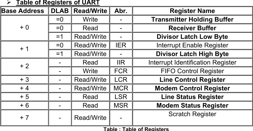
¾ Table of Registers of UART
Base Address DLAB Read/Write Abr. Register Name
=0 Write - Transmitter Holding Buffer
=0 Read - Receiver Buffer
+ 0
=1 Read/Write - Divisor Latch Low Byte
=0 Read/Write IER Interrupt Enable Register
+ 1
=1 Read/Write - Divisor Latch High Byte
- Read IIR Interrupt Identification Register
+ 2
- Write FCR FIFO Control Register
+ 3 - Read/Write LCR Line Control Register
+ 4 - Read/Write MCR Modem Control Register
+ 5 - Read LSR Line Status Register
+ 6 - Read MSR Modem Status Register
[image:1.612.85.527.496.726.2]+ 7 - Read/Write - Scratch Register
2 ¾ DLAB ?
• You will have noticed in the table of registers that there is a DLAB column. When DLAB is set to '0' or '1' some of the registers change. This is how the UART is able to have 12 registers (including the scratch register) through only 8 port addresses.
• DLAB stands for Divisor Latch Access Bit. When DLAB is set to '1' via the
line control register, two registers become available from which you can set your speed of communications measured in bits per second.
• The UART will have a crystal which should oscillate around 1.8432 MHZ. The
UART incorporates a divide by 16 counter which simply divides the incoming
clock signal by 16. Assuming we had the 1.8432 MHZ clock signal, that would leave us with a maximum, 115,200 hertz signal making the UART capable of
transmitting and receiving at 115,200 Bits Per Second (BPS). That would be
fine for some of the faster modems and devices which can handle that speed, but others just wouldn't communicate at all. Therefore the UART is fitted with a
Programmable Baud Rate Generator which is controlled by two registers.
• Ex: Lets say for example we only wanted to communicate at 2400 BPS??
We would have to divide 115,200 by 48 to get a workable 2400 Hertz Clock. The "Divisor", in this case 48, is stored in the two registers controlled by the "Divisor Latch Access Bit". This divisor can be any number, which can be stored in 16 bits (ie 0 to 65535). The UART only has a 8 bit data bus, thus this is where the two registers are used. The first register (Base + 0) when DLAB = 1 stores the "Divisor latch low byte" where as the second register (base + 1 when DLAB = 1) stores the "Divisor latch high byte."
Below is a table of some more common speeds and their divisor latch high bytes & low bytes. Note that all the divisors are shown in Hexadecimal.
Speed (BPS) Divisor (Dec) Divisor Latch High Byte Divisor Latch Low Byte
50 2304 09h 00h
300 384 01h 80h
600 192 00h C0h
2400 48 00h 30h
4800 24 00h 18h
9600 12 00h 0Ch
19200 6 00h 06h
38400 3 00h 03h
57600 2 00h 02h
115200 1 00h 01h
3 ¾ Line Control Register (LCR)
• The Line Control register sets the basic parameters for communication. Bit 7 is the Divisor Latch Access Bit or DLAB for short. We have already talked about what it does. Bit 6 Sets break enable. When active, the TD line goes into "Spacing" state which causes a break in the receiving UART. Setting this bit to '0' Disables the Break.
1 Divisor Latch Access Bit Bit 7
0 Access to Receiver buffer, Transmitter buffer & Interrupt Enable Register
Bit 6 Set Break Enable
Bit 5 Bit 4 Bit 3 Parity Select
X X 0 No Parity
0 0 1 Odd Parity
0 1 1 Even Parity
1 0 1 High Parity (Sticky)
Bits 3, 4 and 5
1 1 1 Low Parity (Sticky)
Length of Stop Bit
0 One Stop Bit
Bit 2
1 2 Stop bits for words of length 6,7 or 8 bits or 1.5 Stop Bits for Word lengths of 5 bits.
Bit 1 Bit 0 Word Length
0 0 5 Bits
0 1 6 Bits
1 0 7 Bits
Bits 0 and 1
1 1 8 Bits
Table: Line Control Register
• Bits 3,4 and 5 select parity. If you study the 3 bits, you will find that bit 3 controls parity. That is, if it is set to '0' then no parity is used, but if it is set to '1' then parity is used. Jumping to bit 5, we can see that it controls sticky parity. Sticky parity is simply when the parity bit is always transmitted and checked as a '1' or '0'. This has very little success in checking for errors as if the first 4 bits contain errors but the sticky parity bit contains the appropriately set bit, then a parity error will not result. Sticky high parity is the use of a '1' for the parity bit, while the opposite, sticky low parity is the use of a '0' for the parity bit.
• If bit 5 controls sticky parity, then turning this bit off must produce normal parity provided bit 3 is still set to '1'. Odd parity is when the parity bit is transmitted as a '1' or '0' so that there is a odd number of 1's. Even parity must then be the parity bit
produces and even number of 1's.
• Bit 2 sets the length of the stop bits. Setting this bit to '0' will produce one stop bit, however setting it to '1' will produce either 1.5 or 2 stop bits depending upon the word length. Note that the receiver only checks the first stop bit.
• Bits 0 and 1 set the word length. This should be pretty straight forward. A word length of 8 bits is most commonly used today.
/Mark
4 ¾ Modem Control Register (MCR)
Bit Notes
Bit 7 Reserved Bit 6 Reserved
Bit 5 Autoflow Control Enabled (16750 only) Bit 4 LoopBack Mode
Bit 3 Aux Output 2 Bit 2 Aux Output 1
Bit 1 Force Request to Send
[image:4.612.133.485.78.227.2]Bit 0 Force Data Terminal Ready
Table: Modem Control Register
• The Modem Control Register is a Read/Write Register. Bits 5,6 and 7 are reserved. Bit 4 activates the loopback mode. In Loopback mode the transmitter serial output is placed into marking state. The receiver serial input is disconnected. The transmitter out is looped back to the receiver in. DSR, CTS, RI & DCD are disconnected. DTR, RTS, OUT1 & OUT2 are connected to the modem control inputs. The modem control output pins are then place in an inactive state. In this mode any data which is placed in the transmitter registers for output is received by the receiver circuitry on the same chip and is available at the receiver buffer. This can be used to test the UARTs operation.
• Aux Output 2 maybe connected to external circuitry which controls the UART-CPU interrupt process. Aux Output 1 is normally disconnected, but on some cards is used to switch between a 1.8432MHZ crystal to a 4MHZ crystal which is used for MIDI. Bits 0 and 1 simply control their relevant data lines. For example setting bit 1 to '1' makes the request to send line active.
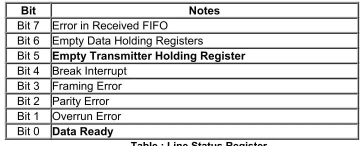
¾ Line Status Register (LSR)
Bit Notes
Bit 7 Error in Received FIFO
Bit 6 Empty Data Holding Registers
Bit 5 Empty Transmitter Holding Register
Bit 4 Break Interrupt Bit 3 Framing Error Bit 2 Parity Error Bit 1 Overrun Error
[image:4.612.124.484.466.612.2]Bit 0 Data Ready
Table : Line Status Register
• The line status register is a read only register. Bit 7 is the error in received FIFO bit. This bit is high when at least one break, parity or framing error has occurred on a byte, which is contained in the FIFO.
5 fashion. The shift register is used to convert the byte to serial, so that it can be
transmitted over one line.
• When bit 5 is set, only the transmitter holding register is empty. So what's the
difference between the two? When bit 6, the transmitter holding and shift registers are empty, no serial conversions are taking place so there should be no activity on the transmit data line. When bit 5 is set, the transmitter holding register is empty, thus another byte can be sent to the data port, but a serial conversion using the shift register may be taking place.
• The break interrupt (Bit 4) occurs when the received data line is held in a logic state '0' (Space) for more than the time it takes to send a full word. That includes the time for the start bit, data bits, parity bits and stop bits.
• A framing error (Bit 3) occurs when the last bit is not a stop bit. This may occur due to a timing error. You will most commonly encounter a framing error when using a null modem linking two computers or a protocol analyzer when the speed at which the data is being sent is different to that of what you have the UART set to receive it at.
• A overrun error normally occurs when your program can't read from the port fast enough. If you don't get an incoming byte out of the register fast enough, and another byte just happens to be received, then the last byte will be lost and a overrun error will result.
• Bit 0 shows data ready, which means that a byte has been received by the UART and is at the receiver buffer ready to be read.
¾ Modem Status Register (MSR)
Bit Notes
Bit 7 Carrier Detect
Bit 6 Ring Indicator
Bit 5 Data Set Ready
Bit 4 Clear To Send
Bit 3 Delta Data Carrier Detect
Bit 2 Trailing Edge Ring Indicator
Bit 1 Delta Data Set Ready
Bit 0 Delta Clear to Send
Table: Modem Status Register
• Bit 0 of the modem status register shows delta clear to send, delta meaning a change in, thus delta clear to send means that there was a change in the clear to send line, since the last read of this register. This is the same for bits 1 and 3.
6 • Bits 4 to 7 show the current state of the data lines when read. Bit 7 shows Carrier
Detect, Bit 6 shows Ring Indicator, Bit 5 shows Data Set Ready & Bit 4 shows the status of the Clear To Send line.
Example Questions:
Ex1: Write the required assembly Language program segment to provide the following frame for serial communication?
- 7 bits character, 1 stop bit, odd parity
Solution: We can provide the above settings by using the Line Control Register.
D7 D6 D5 D4 D3 D2 D1 D0
DLAB Break Parity2 Parity1 Parity0 Stop Data1 Data0
Then, 0000 1010B = 0AH is to be sent to the address of the Line Control Register (base
+03H)
MOV DX,3FBH ;3F8H+03
MOV AL,0AH ;the control data
OUT DX,AL ;issue the control data
Ex2: Program the divisor latch to provide 9600 baud rate. Assume 1.8432 MHz frequency.
16 . .
× =
rate baud
freq clock ref value
Divisor
Divisor value = 1.8432 x 10⁶/(9600 x 16)= 115200/9600=12
Then D7 of the Line Control register must be 1 for accessing DLAB.
MOV AL,80H ;10000000B to access DLAB
MOV DX,3FBH ; the address of the control register (3F8H+03)
OUT DX,AL ;make D7=1 for DLAB
;now send the divisor value
MOV AL,12 ;9600 baud rate
MOV DX,3F8H ; Low byte divisor latch address
00 =5 data bits 01 =6 data bits 10 =7 data bits 11 =8 data bits
0=1 stop bits 1=2 stop bits
XX0 = No parity 001 = Odd parity 011 = Even parity 101 =High parity(sticky) 111=Low parity(sticky)
0=break
1=disable break
1 = Divisor Latch Access Bit
7
OUT DX,AL ;issue the low byte
MOV AL,00
INC DX ;high byte divisor latch address(3F8H+01)
OUT DX,AL
•
Transmitting Serial data
The following procedure is used to transmit serial data using the Serial port.
1. set DTR & RTS (DTR-Data Terminal Ready & RTS-Request To Send) (write 0000 0011B to the Modem Control register at base address+04 )
2. check DSR & CTS (DSR-Data Set Ready & CTS-Clear to send) (check if bits 5 & 4 in the Modem Status register are equal to 1 at base address+06) wait until timeout
3. check if Transmitter Holding Register (bit 5 of Line Status register) is Empty
(empty means ready for a byte/ is bit 5 is equal to1 at base address+5) wait until timeout
4. write the byte to data register (Transmitter Holding Buffer)
(Transmitter holding buffer is at base address+00/ the parallel data in
transmitter holding buffer is transferred into transmit shift register to provide serial transmit)
•
Receiving Serial Data
The following procedure is used to receive serial data using the Serial port.
1. set DTR (DTR-Data Terminal Ready) (write 0000 0001B to the Modem Control register)
2. check DSR (DSR-Data Set Ready) (check if bits 5 of the Modem Status Register) wait until timeout
3. check if Data is Ready(bit 0 of Line Status Register)
(Data ready means that data has been received and is at the receiver buffer to be read)
wait until timeout
4. read the byte from data register (Receiver Buffer)
(Receiver Buffer is at the base address+00)
REFERENCE: