International Journal of Innovative Technology and Exploring Engineering (IJITEE) ISSN: 2278-3075, Volume-8 Issue-10, August 2019
Design and Implementation of Real Time Data
Acquisition System in All Programmable System
on Chip
P.Suresh, U.Saravanakumar, V.Karthikeyan, G.Vamsi Krishna, K.Sreekanth, G.Kumar Reddy
Abstract: In the recent era, the world has faced drastic improvement in automation industries and there is an need of speedy multi-functional system with higher performance device. The demand for faster, smaller and energy efficient computing systems for miniaturized devices is tremendously increased day by day. Over the past decades, there is a drastic change in semiconductor industry due to its advantages and higher performance of integrated circuits even there is more complexity in design and more expensive. The semiconductor industry started to embrace new design and reuse policies are mutually discussed as system-on-chip (SoC) design. This technology allows to develop a system with higher performance only with required blocks for different applications. In this paper, it is proposed to implement SoC based data acquisition system to measure the atmospheric parameters with different sensors in real time.
I. INTRODUCTION
In recent years the System on Chip (SoC) plays a major role in semiconductor industry due its promising technological advantages on successful implementation. Most of the researchers involved in Very large Scale Integrated (VLSI) circuit design have turned towards the SoC from Application Specific Integrated Circuits (ASIC). The customized SoC for variety of application from commercial to industrial applications includes a microprocessor, memory and along with peripherals in a compact size. Recently remarkable achievements has been reported by most of the researchers in the proposed rea of research in an attainable thickness level on VLSI circuits [1]. The researchers, design engineers keep hop continuously on improving the existing techniques and to propose new technological innovation an integration to manage and overcome the complexity in the VLSI circuits due to its promising achievements. In the semiconductor industry one such development is SoC, where’s the complete framework is available as intellectual property (IP) blocks, IP cores, or virtual components from the different vendors in the reusable format to develop any kind of applications. The available IP cores in the reusable format are embedded processors blocks, different memory blocks, analog circuitry blocks, digital circuitry blocks, peripheral interface blocks, components, etc, which is required to design,
Revised Manuscript Received on May 30, 2019.
P.Suresh, (Senior Member IEEE), Dept. of ECE, Vel Tech Rangarajan Dr. Sagunthala R&D Institute of Science and Technology, Tamilnadu, India
U.Saravanakumar, (Senior Member IEEE), Dept of ECE, Muthayammal Engineering College, Namakkal, Tamilnadu, India
V.Karthikeyan, RF Application Engineera, Scientific Society Group, Tamilnadu, India
G.Vamsi Krishna, Dept. of ECE, Vel Tech Rangarajan Dr. Sagunthala R&D Institute of Science and Technology, Tamilnadu, India
K. Sreekanth, Dept. of ECE, Vel Tech Rangarajan Dr. Sagunthala R&D Institute of Science and Technology, Tamilnadu, India
G.Kumar Reddy, Dept. of ECE, Vel Tech Rangarajan Dr. Sagunthala R&D Institute of Science and Technology, Tamilnadu, India
development and implementation for a specific function [2]. The current technology and the software packages allow the developer to reuse the real time operating system, kernels, device drivers, library files, etc., This reusable IP cores, IP blocks, etc., reduces the developing time of the designer on using verifiable reusable blocks obtained from authorized vendors. The technology allows to create new IP blocks for specific application in the for of SoC and the same has be put in to market with some authentication followed by semiconductor industry in the reusable format. The integration of adopted reusable IP blocks is the major task for any application to the designers. The integration involves communication between IP blocks, mapping of ports and pins specified by the vendor and implementing to verify, validate the design for desired application. More and more integration of reusable IP blocks increases the complexity of the design and the same has to be modified based on the requirements to meet the objective without any flaws with respect to Moore’s Law and it is the challenging task to designers.
Recently there is a drastic improvement in the semiconductor industry and the technologies allows to bring the world into small hand. Field Programmable Gate Array (FPGA) is a chip which holds millions of transistors to create the desired module which allow the designer to use as a single module or multiple module in the same chip and it is highly enough to implement most of the applications from commercial to industrials. Recently the current FPGA has several millions of transistors in it, which allows to adopt the multiple processors and multiple peripherals, etc., and it is adequate to implement Multi-Processor Systems-on-Chip (MPSoCs) for variety of applications which includes prototyping of hardware accelerators such as image processing [6], encryption [7], molecular dynamics [8], Networks-on-Chip (NoCs) [10], space applications, defence applications, etc.,. and the same is represented as All Programmable System on Chip (APSoC).
Over the years, there is huge adoption of SoC due to its advantages and its flexibility id design and reusability attracts more researchers in the semiconductor industry with higher complexity in industrial standards. Most of the industries switching to SoC design for all needs due to higher performance and lower power utilization instead of manufacturing discrete devices for example bus interfaces [14], peripherals, IP protection and tracking [15], and test wrappers [16], analog devices, digital devices, etc.,. Day by day there is huge improvement in semiconductor industry and much more IP blocks are produced from different vendors either in free of cost or with nominal charges for reusable and its highly competitive and demanding
circumstances among
Obviously, SoC structures are huge, complex plans that require broad testing and confirmation. To accomplish this, the item advancement procedure must guarantee the item determination stage is coordinated easily with the item configuration stage, permitting the client's requests, promoting objectives and originator mastery, to be assessed and broke down at fundamentally less expense in time and assets, and the final product need to be incorporated rapidly. In this paper in order to express the technological advance of APSoC, it is proposed to monitor the atmospheric parameter under monitoring. The paper is organized in such a way as follows, the reusability of IP block is discussed in section II, adopting IP core reusability for desired application to make single chip is discussed in section III and achievement on design and implementation is concluded in section IV.
II. SYSTEM-LEVEL DESIGN
In recent years the technology reached too high in the semiconductor industry, which encourages the researchers to concentrate more on Modern electronic systems with respect to ITRS standards. It also increases the design complexity and encourages the developers to make the combination of different types of components: microcontrollers, microprocessors, DAC, peripherals, DSPs, memories, etc. With the increase in technology and features, the designers also need to consider the demands for lesser development cost, lower design time, area reduction. The designer have dedicated target to make the design foe the desired application with the necessary modules with their abstraction levels called as System Level Design (SLD)[18]. The SLD involves both hardware and software design process like modelling, partitioning, integration, synthesis, verification and validation of the complete system. The design and implementation have several levels of abstraction in its implementation with higher complexity. The design complexity increases the hardware design cost, on verification in software emulation which reduces the design cost with the advantages of verification in emulation environment. There are different languages involved to reduce the design complexity with the technology advancement and increases the utilization of compact design with higher complexity. The reality is the degree of most noteworthy deliberation will be the one that endures, and that is plainly the product space. Thinking about the monetary reality, this progress won't be unexpected, yet it will happen more as an advancement than an insurgency. The in all probability change will be along the lines that product pursued as it advanced from an exacting utilization of hand-coded constructing agent in the fifties to broad utilization of compilers in the sixties. The most reasonable situation will begin by moving the non-basic segments of time-to-advertise driven plans to higher levels. At that point, logically after some time, progressively advanced compiler and blend innovation enlarged by expanding equipment usefulness will broaden the span of programmed strategies until just incredibly basic segments of exceedingly execution driven plans will be actualized at the register transfer level. The design flow process for hardware and software leads to reduction in design technology and reduces its cost. In fore coming days optimally may leads to reduction in implementation with compiler environment.
successfully and leads too design process simplification with reduced complexity in SOC [19].
III. SYSTEM ON CHIP ARCHITECTURE
Improving the energy efficiency of the computing system is presently one of the most important problems in embedded system architecture among the designers and academic researchers. The energy consumption of the computing system is purely depends on physical design of the fabricated chip and it is the challenging task when more number of blocks to be added into a single chip [20]. With the advancement in chip fabrication technology, embedded systems can be developed into a single chip by incorporating required features on board as IP blocks which meets designer specifications. This development improves the performance of computing systems with reduced size and less power consumption.
Due to high complexity in sensitivity of analog/mixed signal design configuration leads to degrade the performance of commonly used IP blocks. There are different types of IP blocks available which is very hard to find and have design complexity for hard IP blocks in reuse. The package released by vendors will have their own reusable Hard, soft and firm IP blocks which is readily available in market with nominal price for reusability to make efficient design. System on Chip (SoC) is a collection module which has all kinds of components and subsystems those are appropriately interconnected in a single chip which perform the specified functionality by the end users.
The main role of this System on Chip is collecting the parameters values from the different sensors mentioned above and do the necessary data processing to get the real values. The processed parameters are then transmitted to the atmospheric parameter monitoring system.
IV. EXPERIMENTAL RESULTS AND
DISCUSSION
In this work it is addressed to implement practically the data acquisitions system to evaluate the performance of the proposed system level design with All Programmable System on Chip. The performance of the APSoC based data acquisition system was simulated in Vivado design suite environment and implemented in Digilent Zybo Board. Initially, the architecture have been developed and the availability of required IP blocks has been verified with the developing package available for the proposed system. The available reusable required IP block is adopted; modified; replaced for implementation on FPGA board in real time for the proposed data acquisition system. The proposed design with its implementation is discussed in following section and also concluded the achievements for the proposed work with detailed summary.
V. HARDWARE AND SOFTWARE
PLATFORMS
The detailed description of the proposed architecture and its design is presented in this section. The proposed architecture is designed in FPGA
platform, Zybo FPGA
International Journal of Innovative Technology and Exploring Engineering (IJITEE) ISSN: 2278-3075, Volume-8 Issue-10, August 2019
[image:3.595.97.502.65.350.2]with required peripherals in it is shown in Figure 1.
Figure 1. Digilent Zybo board
The Digilent ZYBO board is a development board designed in compatible with Xilinx's new high-performance Vivado Design Suite to create softcore and hardcore processor to implement the real time code with toolset ISE/EDK environment. The toolsets create platform for FPGA logic design to implement an embedded ARM software development environment with simplified design flow. Any type of system from simpler to higher complexity with real time operating system running at different environment with different peripherals is possible in the proposed platform. A
simple embedded piece of code with lesser complexity can be written and downloaded with the required peripherals IP blocks. In future if any changes in design or if any additional features need to be included is possible simpler modification in reusable IP blocks.
The proposed data acquisition system is to collect the environmental atmospheric data through the sensor interfaced with required peripherals. In the proposed system it planned to develop ARM Cortex 32 bit RISC processor (ZynQ Processing System) implemented in FPGA platform.
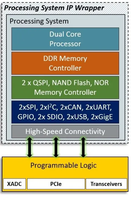
[image:3.595.108.536.500.761.2]Figure 2 shown the development of proposed architecture with ZynQ processing system with required peripheral blocks like clock pulse, UART, Timer, interconnect device, analog to digital converter, required GPIO’s, etc along with PMOD to interface sensors. The proposed architecture is implemented using modern package Xilinx EDK 16.4, it has Xilinx ZynQ processing system as reusable IP blocks which can be modified by the designer based on the requirements and features [22], with the additional required building blocks. The processing system is implemented in SDK software environment with the building blocks as reusable IP soft cores. On successful verification of proposed application in software environment, the same can be implemented in hardware FPGA chip. The developed and implemented Zynq-7000 processing system is shown in Figure 3.
The Zynq-7000 family consists of a system-on-chip (SoC) style integrated processing system (PS) and a Programmable Logic (PL) unit, providing an extensible and flexible SoC solution.
Figure 3. Zynq-7000 Processing System
Performance evaluation of the DAS in FPGA
The DAS system is developed with required FPGA IP Core for proposed system in the EDK environment. Upon successful generation of bitstream for the customizable architecture of proposed system, it is exported in to hardware implementation through the eclipse SDK to program FPGA.
The DAS system is implemented in target FPGA platform in Zybo board through Xilinx Vivado and eclipse Software
[image:4.595.64.278.300.627.2]displayed in Teraterm HyperTerminal and it is shown in Figure 4.
Figure 4. Atmospheric data monitoring in Teraterm HyperTerminal.
VI. CONCLUSION
In this paper a Data Acquisition System is proposed to implement the system in FPGA-based multicore architectures platform with ZynQ processing System, which is based on task-level pipelining (TaLP) in the context. The implementation is customized with required features in processing elements, based on the high-level synthesis design flow model. The generated hardware bitstream is downloaded in FPGA board, the backend C++ high level code is to verify the architecture. The physical sensor is interfaced with FPGA board through PMODs on the implemented hardware architecture (Zynq Processing System). The real time implementation to monitor the atmospheric condition is successfully evaluated in HyperTerminal. The evaluation on the real FPGA system shows how physical sensors can be attached to the Zynq processing system without loss of sensor data. Further sensor data will be evaluated in future, with the target to enlarge the application area of the presented approach. In case of sensor failure, the defect sensor can be excluded from the measurement without an interruption of this, which will improve the system reliability.
REFERENCES
1. International Techbology Roadmap for Semiconductors. [Online]. Available: http://www.public.itrs.net.
2. M. Keating and P. Bricaud, Reuse Methodology Manual: For System-on-a-Chip Designs, 3rd ed. Boston, MA: Kluwer, 2002.
3. R. Rajsuman, System-on-a-Chip Design and Test. Boston, MA: Kluwer, 2000.
4. H. Chang, L. Cooke, M. Hunt, G. Martin, A. McNelly, and L. Todd, Surviving the SOC Revolution: A Guide to Platform-Based Design. Boston, MA: Kluwer, 1999.
5. G. Moore, BCramming more components onto integrated circuits,[ Electronics, vol. 38, pp. 114–117, Apr. 19, 1965.
International Journal of Innovative Technology and Exploring Engineering (IJITEE) ISSN: 2278-3075, Volume-8 Issue-10, August 2019
7. O. Nibouche, “Fast Architectures for FPGA-Based Implementation of RSA Encryption Algorithm,” Proc. FPT’04, pp. 271-278, Dec. ‘04. 8. Y. Gu, and M. Herbordt, “FPGA-Based Multigrid Computation for
Molecular Dynamics Simulations,” Proc. IEEE FCCM Symp., Apr. ‘07.
9. B. Fort, D. Capalija, Z. Vranesic, and S. Brown, “A Multithreaded Soft Processor for SoPC Area Reduction,” Proc. IEEE FCCM Symp., pp. 131-142, Apr. ‘06.
10. P. Wolkotte, G. Smit, and J. Becker, “Energy-Efficient NoC for Best Effort Communication,” in Proc. FPL’05, pp. 197-202, Aug. ‘05. 11. A. Patel, M. Saldana, C. Comis, P. Chow, “A Scalable FPGA-based
Multiprocessor, “Proc. IEEE FCCM Symp., pp. 111-120, Apr. ‘06. 12. A. Chandrakasan and R. Brodersen, Low Power Digital CMOS
Design. Boston, MA: Kluwer, 1995.
13. Open Core Protocol Specification 2.1. OCP-IP Assoc. [Online]. Available: http://www.ocpip.org.
14. Virtual Socket Interface Alliance. [Online]. Available: http://www.vsi.org.
15. M. Richhetti, BOverview of proposed IEEE P1500 scalable architecture for testing embedded cores (slide presentation, presented at the Design Automation Conf., Las Vegas, NV, 2001, pp. 1–26.
16. IEEE 1500 Standard. [Online]. Available:
http://www.grouper.ieee.org/groups/1500.
17. R. Tummala and V. Madisetti, B System on chip or system on package?[. IEEE Des. Test Comput., vol. 16, no. 2, pp. 48–56, Apr.– Jun. 1999.
18. S. E. Schultz, “The New System-Level Design Language”, Integrated System Design, July 1998.
19. A.A. Jerraya, M. Romdhani, Ph. Le Marrec, F. Hessel, P. Coste, C. Valderrama, G. F. Marchioro, J.M. Daveau,and N.-E. Zergainoh, “Multi-language Specification for System Design and Codesign”, System Level Synthesis, Kluwer Academic Publishers, 1999. 20. C.-W. Wu, “SOC testing methodology and practice,” in Proc. Design,
Automation and Test in Europe (DATE), Munich, Mar. 2005. 21. Zybo Board Reference Manual, Digilent, Inc, 2013.