Introduction
As the development of miniaturized systems based on the so-called lab-on-a-chip technology increases across a wide and diverse range of applications, the choice of materials and appropriate fabri-cation techniques is constantly under evaluation by the academic and industrial communities.1–5 One of the main drivers behind such work lies in the fact that when micrometer-scale fluidic channels are used, they have a high surface-to-volume ratio compared with more con-ventional (1 cm) vessels. As an analogy, when the dimension of a cube is reduced from 1 mm to 1 µm, the surface-to-volume ratio increases by a factor of a thousand.
The high surface area in microfluidic channels may influence the processes being performed within such a system. Clearly this attribute of microfluidic sys-tems can be a positive factor. High surface area could lead to the opportunity, for ex-ample, of exploiting relatively simple surface-dependent electrokinetic modes
of pumping (electro-osmosis) and efficient component-separation methodologies (based on differential electrophoretic mobilities of charged analyte species). Furthermore, by using chemically or bio-logically modified surfaces, it becomes possible to mediate processes within the unique spatial and temporal domains of a microfluidic device; this could offer new and exciting routes to chemical and bio-logical processing.6–8
There is, of course, another side to the coin; the inappropriate selection of device materials can lead to the severe disruption and failure of a process that may be rela-tively straightforward in a larger vessel of the same material where the surface-to-volume ratio has a much smaller influence on the process being performed. To fully realize the potential of lab-on-a-chip methodology, it is important to consider the advantages and disadvantages of se-lecting materials and fabrication tech-niques to produce the required channel
tion methods (photolithography and wet etching) used in developing lab-on-a-chip–type devices were adopted from those used by the semiconductor industry to develop microelectromechanical sys-tems (MEMS). Accordingly, early mi-crofluidic devices were manufactured in silicon.1,9An obvious follow-on from sili-con was the use of glass. This resulted in devices being produced in common silica glass, Pyrex and quartz, into which chan-nel networks were etched using similar methodologies as those used for silicon.10 This in turn led to the generation of com-bined silicon/glass devices, which offered chemical robustness, optical transparency, and the possibility of integrating mechan-ical parts with fluidic systems for fluidic control. In reality, such systems can be both technically demanding and expen-sive to fabricate, and while such systems are still being developed, there has been growing interest in the use of molded fab-rication techniques. These techniques offer relatively simple, rapid, and inex-pensive high-throughput production, which has led to the greater use of polymer-based systems. This trend can be gauged from the rapidly increasing number of publications in which polymers are being used for chip fabrication, particularly for aqueous-based applications.
However, selecting the most suitable material to enhance process performance for a specific application, rather than just simplify fabrication, is no trivial task. A number of material properties have to be taken into account, such as mechanical strength, thermal stability, chemical inert-ness, optical transmission, electrical insu-lation, and dielectric and surface properties. In addition, operational parameters such as the choice of solvent, temperatures, and pressure will need to be considered when selecting a suitable substrate. The aim of this article is to review the common types of materials that are currently used to fab-ricate microfluidic devices and consider how these influence the eventual perform-ance of the final device. In particular, the physical, chemical, and biological attrib-utes of such materials will be considered, as these will ultimately lead to the future generation of more highly functionalized and integrated systems.
Materials Currently Used for Chip
Fabrication and Their Properties
A number of materials, including sili-con, quartz, glass, metal, and polymers, have been used to date to fabricate
mi-M
aterials Matter in
Microfluidic
Devices
Xunli Zhang and Stephen J. Haswell
Abstract
As more micro- and nanofluidic methodologies are developed for a growing number of diverse applications, it becomes increasingly apparent that the choice of substrate material can have a profound effect on the eventual performance of a device. This is due mostly to the high surface-to-volume ratio that exists within such small structures. In addition to the obvious limitations related to the choice of solvent, operating temperatures, and pressure, the method of fluidic pumping—in particular, an electrokinetics-based methodology using a combination of electro-osmotic and electrophoresis flows—can further complicate material choice. These factors, however, are only part of the problem; once chemicals or biological materials (e.g., proteins or cells) are introduced into a microfluidic system, surface characteristics will have a profound influence on the activity of such components, which will subsequently influence their performance. This article reviews the common types of materials that are currently used to fabricate microfluidic devices and considers how these materials may influence the overall performance associated with chemical and biological processing.
Consideration will also be given to the selection of materials and surface modifications that can aid in exploiting the high surface properties to enhance process performance.
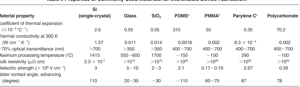
crofluidic devices.11 Table I summarizes some of the more general properties of these substrates.12
As indicated previously, silicon has been widely used for a range of MEMS and bio-MEMS13applications and will be discussed by Jensen in this issue. How-ever, the semiconductive properties of sil-icon can be limiting in some microfluidic applications, most notably in supporting voltage-driven pumping using a combina-tion of electro-osmotic and electrophoresis flows, where the electro-osmotic flow (EOF) requires an electrical double layer to be formed in the region of the solid/liq-uid interface. When performing chemical reactions in non-aqueous solvent systems, glass has proved to be an excellent choice of substrate due to its chemical and ther-mal resistance and its optical trans-parency, which enables on-chip detection to be carried out with relative ease.2,4In addition, the presence of inherent native surface charges makes glass most suitable for supporting electro-osmotic flow.4This surface property is also present in a num-ber of polymer materials such as poly(di-methylsiloxane) (PDMS), an elastomeric and optically transparent polymer, which has proven to be a popular material for its low cost and fast prototyping. How-ever, the porosity of PDMS can be prob-lematic, as it will absorb species (e.g., dyes) from solutions and will swell ac-cordingly in most non-aqueous solvents. In contrast, the gas permeability and me-chanical properties of PDMS make it an excellent material for exchanging gases, for example, in a device supporting living cells, which usually require gases for their biological activity, and it can be used to construct valves and displacement pumps.
In order to produce chemically stable polymer chips while retaining a relatively
simple fabrication methodology, researchers are continually testing new polymeric materials in microfluidic applications. One good example is cyclic olefin copoly-mers (COCs), which are claimed to offer significant advantages over poly(methyl methacrylate) and polycarbonate, which is a group of relatively hard plastics.14 These advantages include low water absorption; chemical and physical resis-tance to most polar solvents such as ace-tone, methanol, and isopropyl alcohol; and a significantly wide UV transmit-tance, which is beneficial for on-chip optical detection. As with most polymers, however, the inherent disadvantages of low melting points and susceptibility to chemical attack of COCs still limit their use.
In general, selecting a material for a specific microfluidic application requires some degree of compromise; therefore, careful consideration of its physical and chemical properties is essential. For in-stance, mechanical properties are impor-tant for fabrication and pressure-based operation, and optical properties are relevant if imaging or on-chip detection is required. Electric/dielectric properties are also important factors to consider if electro-osmotic–based pumping and electrokinetic separations are required. In addition, the wetting properties and contacts between the surface and the sample, in particular for biological samples such as cells, may be of primary importance. Thus, an understanding of the inherent properties of the materials used in developing microfluidic devices, which might include composites, will not only assist in the selection of an appropriate material and fabrication method, but also help optimize the opera-tional conditions of the process being controlled.
Exploiting the High
Surface-to-Volume Ratio of Microfluidic
Devices
In this section, examples of how surface charge is used to exploit electrokinetic pumping and chemical/biological surface functionalization will be considered, as these represent the two main areas of cur-rent use related to material properties.
Electro-Osmotic Flow (EOF)
Pumping solutions through a channel network by electro-osmotic flow (EOF), using voltages applied via electrodes placed in reservoirs, has several signifi-cant advantages over alternative pumping methods.15,16This type of pumping system can be easily miniaturized, because no mechanical moving parts are involved and the required voltage sequences can be readily applied under automated computer control.
For glass and many polymer-based microfluidic reactors, the channel wall– solution interface normally has a negative charge. This immobile surface charge at-tracts a diffuse layer (on the order of nanometers in thickness) of mobile, oppo-sitely charged counterions in the solution adjacent to the channel wall (cations for a negatively charged glass channel wall). Upon the application of an electric field along the channel length, the nanometer-thick “skin” of mobile cations migrates to-ward the more negative electrode and drags all the intervening solution in the bulk of the channel with it.17–19
[image:2.612.50.564.567.717.2]An important feature of EOF is that the liquid EOF velocity is constant across the channel, except in the nanometer-thick re-gions of the diffuse layer of counterions very close to the wall. Unlike EOF, which has plug flow (enabling all fluid across the channel to have the same flow velocity), pressure-driven flow produces a parabolic
Table I: Properties of Commonly Used Materials for Microfluidic Device Fabrication.12
Si
Material property (single-crystal) Glass SiO2 PDMSa PMMAb Parylene Cc Polycarbonate
Coefficient of thermal expansion
2.6 0.55 0.55 310 55 0.35 70.2
Thermal conductivity at 300 K
(W ) 1.57 0.011 0.014 0.0018 0.002 8.3 104 0.002
70% optical transmittance (nm) 700 350 350 400 700 400 700 400 700 400 700 Maximum processing temperature (C) 1415 550 600 1700 150 100 290 100 Bulk resistivity ( cm) 2.3 1011 1010 1010 1020 1020 1020 1020 Dielectric strength (106V cm1) 3 5 10 2 3 2.1 0.17 0.19 2.67 0.39 Water contact angle, advancing
(degree) 110 20 35 30 110 60 75 87 78
aPDMS: poly(dimethylsiloxane).bPMMA: poly(methyl methacrylate).cParylene C: poly-para-xylylene.
velocity profile, with high velocities in the channel center and slow velocities near the wall, giving rise to increased “blur-ring” of reagent zones along a channel length (i.e., dispersion). The imaging of velocity profiles induced by EOF and pressure-driven flow has been described well by Paul et al.20
The EOF fluid velocityveofis given by Equation 1:
, (1)
where Eis the electric field (voltage di-vided by electrode separation), εis the rel-ative dielectric constant of the liquid, ε0is the permittivity of free space, ζis the zeta potential of the channel wall–solution in-terface, and ηis the liquid viscosity.17–19It can be seen from Equation 1 that veof is proportional to the applied voltage and depends on the properties of both the liq-uid and the channel material. EOF is not obtained with semiconductor materials such as silicon and does not occur with low-polarity solvents such as alkanes, where no diffuse layer of surface counter-ions exists. The EOF linear velocity veofis independent of the channel cross-sectional dimensions, whereas the EOF volumetric flow rate (given by the product of veof mul-tiplied by the channel cross-sectional area) does depend on the channel dimensions. Another benefit to the use of electric fields to control flow is the potential for separation based on species with different charges that have different electrophoretic velocity, veph:
, (2)
where zeis the electronic charge on the species, Dis diffusion coefficient, kis the Boltzmann constant, and T is absolute temperature.
The magnitude of vephfor typical micro-reactor operating voltages is commonly comparable with veof. Thus, the total ve-locity of a charged species is given by the vector sum ofvephand veof. The direction of EOF for aqueous solutions in a glass mi-croreactor is normally toward the more negative electrode, where the glass surface is naturally negatively charged, whereas for a cationic solute species, vephwill be in the same direction as veof(i.e., toward the more negative electrode) and will move faster down the channel than the solvent and neutral species. Anionic solutes will be retarded and may move in the opposite direction, if the magnitude of veph is greater than veof. In this way, elec-trophoretic separation of solutes occurs
veph
zeED kT veof
Eεε0
along with EOF in the microreactor chan-nels when operated under electrokinetic control. The ability to use electrophoretic mobility to spatially locate charged reagents and products within a microfluidic reactor independently of the solvent forms a use-ful aspect of reaction control.16Differential electrophoretic mobilities have been ex-ploited to selectively control product de-tection in the capillary, leading to the technique of electrophoretically mediated microanalysis,21,22which forms the basis of the DNA chip.
Surface Functionalization
The relatively large surface area within microfluidic structures can be exploited in a proactive way to add chemical or biologi-cal functionalization to a process, thus ex-ploiting the spatial and temporal properties of this laminar-flow, diffusive mixing sys-tem. A range of surface-modification tech-niques has been developed, in general, for the following purposes:
1. To alter the electric charge on surfaces.
This is normally carried out by either plasma treatment, coating surfaces with silanizing agents, or both. By changing the surface charge, the EOF direction is altered to control the sample delivery within the channel network.5 Furthermore, pattern-ing the channel surface with different charges can result in some counter/con-flict flows within the channel, which can significantly improve mixing. Counter flow refers to the bulk flowing in opposite directions and conflict flow to a virtual turbulent flow within a flow stream.23 Under different plasma-treatment condi-tions, the surface charge24 and/or the contact angle can be changed, either tem-porarily or permanently.25,26Coating sur-faces with specific chemical groups has also been used to change surface charge.27
2. Surface wetting.By selectively coating the surface with either hydrophilic or hy-drophobic groups, the contact behavior of reagents with the surface is changed in a controllable format. This is done by the commonly used silanization reaction be-tween the surface and the silanizing agent where the silicate of the glass, for instance, reacts with silanes to form a layer of func-tional groups such as amino groups (NH2–) on the glass surface. The selective coating has been applied to generate and control multiphase fluid movement along microchannels.27
3. Surface modification with specific biological functions to bind different biological molecules.A multistep treat-ment of the surface is generally required. First, a layer of a chemical coating such as amino groups is created. Then, it is bio-functionalized by binding biological
molecules, for instance, antibodies. Fi-nally, uncoated sites are blocked to pre-vent nonspecific adsorption. This technique has been extensively used in immunoassay12 and DNA arrays on glass microscope slides.28 Based on the same principle, the surface within microchannels can be modified in situ,and this technique is increasingly attracting attention follow-ing the pioneerfollow-ing work by Whitesides et al.29–31Early results indicate that micro-fluidic biomodification can promise a con-tinuous, faster, flexible tool for bioanalysis.
4. Adding an additional surface.While a high ratio of surface to volume is inherent in an empty/open microchannel, this characteristic may be further pronounced by adding high-surface-area materials such as beads,7pillars, and carbon nano-tubes within the flow path. The introduc-tion of microbeads within narrow channels can cause more difficulties in chip fabrica-tion, especially for bead handling. At-tempts have been made to fabricate reproducible bead-packed chips that use a retaining feature in microchannels to trap beads to a specific area.7,32
The use of silica and polymer mono-liths33–35can also significantly increase the ratio of surface area to volume. In addi-tion, porous monoliths can be equipped to comprise reactive functionalities such as catalytically active sites or even reactants, which enter into and are altered in the course of a chemical reaction, to perform specific chemical or biochemical reactions.33 However, two problems may be en-countered during the operation: (1) a short-cut flow may exist, where the liquid flows through short-cut paths as streams instead of an even distribution over the porous monoliths; and (2) the monolith may not be completely functionalized with reagents. These problems are mainly due to the unevenly distributed structures within the porous monoliths and can be overcome by using in situpolymerization, where the functionalized monomer is in-troduced into the microchannel and then polymerized under curing conditions, for example, exposure to UV light.34,35
It should be noted that rather than ex-ploiting the proactive aspects of a surface, it is equally valid to mask or negate wall effects by fluidically isolating the sample from the substrate channel wall to elimi-nate surface effects. This is carried out by using either a coaxial flow to keep the sample in the center,36 or multiple flow streams surrounding the sample stream to form a “sheath.”37,38
such as photolithography, hot embossing, powder blasting, injection molding, and laser microforming are available.39
Photolithography and Chemical
Etching
For glass microfluidic devices, photo-lithographic fabrication of channel net-works is commonly used.10,40 First, the channel network is designed and printed using suitable computer drawing soft-ware. A negative of the desired final size is then prepared by photoreduction to form the optical mask. Commercially available borosilicate glass photolithographic plates coated with a thin metal etch mask layer (normally chromium) plus an upper layer of positive photoresist (0.5–2.0 µm thick) can be used for channel network fabrica-tion. The pattern of interconnecting chan-nels is transferred from the optical mask to the photoresist layer on the glass. After light exposure, the photoresist is devel-oped and removed, together with the chromium layer, to reveal the areas of glass to be etched. The channels may be etched, for example, using a mixture of 1% HF and 5% NH4F in water at 65°C, resulting in an etch rate of typically 0.3–0.5 µm min–1. During the etch process, it is important that the system be well agitated to ensure a consistent supply of etchant to the surface and the efficient removal of etch debris.
The etched plate containing the channel network must next be sealed by bonding to an upper plate, made of the same glass and containing pre-drilled holes to link to the reagent supply tubing. In our labora-tories, the upper plate is aligned with the channel geometry and thermally bonded to the base plate (typically at 575°C for 3 h). Thermal bonding is aided by placing a weighting block of nonadhering quartz of high softening temperature on the upper plate. A photograph of a microreactor as-sembled in this way is shown in Figure 1 with ceramic adaptors, enabling HPLC (high-performance liquid chromatogra-phy)-type fittings to be connected directly to the chip. In addition to etching channel networks on the substrate surface, this technique can also be used to make molds.
Molding
Molding techniques are an attractive method of fabricating microfluidic de-vices from polymers and plastic due to the ease of production, the reusability of the mold, and the concomitant reduction in fabrication time and costs.10,40
Upon construction of silicon or glass molds, as described earlier, the channel network can be produced on the surface of plastic substrates by a range of molding techniques such as hot embossing, flow
injection, and casting. Channels on PDMS substrates can be easily fabricated by pouring a mixture of the curing agent and the base oligomers over the silicon or glass mold. Once cured, the polymer forms a firm block, with the channel network molded into the surface. The PDMS struc-ture is then peeled away from the mold. Fluid access holes are created by punching through the PDMS block, which is then bonded irreversibly following plasma treatment to a glass cover sheet to close the channel. An alternative way to close the channel network fabricated on PDMS blocks is to use a simple “clamp” and cover sheet, either glass or plastic, to make the PDMS block an operational fluid-tight assembled unit, which can be reopened if necessary.41
Fabrication in polymeric materials, while attractive from an engineering and cost perspective, does pose a number of reagent compatibility issues, as some or-ganic solvents such as acetone can interact with polymers and damage the structure. However, it has been demonstrated that devices containing channels fabricated using photolithography from an epoxy resin such as SU-8 coated onto a polymer support such as methacrylate are relatively robust to chemical attack. This methodol-ogy has the advantage that the non-wetted bulk of the chip can be fabricated from low-cost commodity polymers.42
Summary
The selection of a suitable substrate ma-terial undoubtedly plays a large role in the development and advancement of micro-and nanofluidic systems. Such materials can contribute directly to the fluidic mech-anisms of pumping and separation and the effectiveness of the chemistry and bi-ology within such devices. Important con-siderations in material choice include chemical compatibility, ease and
repro-ducibility of fabrication, compatibility with detection methods, and (if relevant to the application) whether the material sup-ports electro-osmotic flow (EOF) with the solvents of interest. The advantages gained from an inherently high surface-to-volume ratio can be further enhanced with surface-modification techniques to improve chemi-cal or biologichemi-cal robustness and improve flow, pumping, and mixing performance within the device. With advances in fabri-cation technology and materials, the de-velopment of microfluidic-based systems will lead to their wide application in bio/chemical analysis, chemical synthesis, cell manipulation, biomedical monitoring, and point-of-care clinical diagnostics.
References
1. A. Manz, J.C. Fettinger, E. Verpoorte, H. Ludi, H.M. Widmer, and D.J. Harrison,
Trends Anal. Chem.10(1991) p. 144.
2. A. Manz and H. Becker, Eds., Microsystem Technology in Chemistry and Life Sciences
(Springer, Berlin, 1998).
3. K.F. Jensen, Chem. Eng. Sci.56(2001) p. 293. 4. P.D.I. Fletcher, S.J. Haswell, E. Pombo-Villar, B.H. Warrington, P. Watts, SY.F. Wong, and X. Zhang, Tetrahedron58(2002) p. 4735.
5. T. Laurell, J. Nilsson, K. Jensen, D.J. Harrison, and J.P. Kutter, Eds., 8th Int. Conf. Miniaturized Systems for Chemistry and Life Sciences (MicroTAS 2004) (Malmö, Sweden, September 26–30, 2004).
6. C. Wiles, P. Watts, and S.J. Haswell,
Tetrahedron61(2005) p. 5209.
7. P. He, S.J. Haswell, and P.D.I. Fletcher, Lab Chip4(2004) p. 38.
8. C. Wiles, P. Watts, S.J. Haswell, and E. Pombo-Villar, Lab Chip4(2004) p. 171. 9. S.C. Terry, J.H. Jerman, and J.B. Angell, IEEE Trans. Electron. DevicesED-26(1979) p. 1880. 10. T. McCreedy, Anal. Chim. Acta427(2001) p. 39.
11. W. Ehrfeld, V. Hessel, and H. Löwe,
[image:4.612.227.560.82.234.2]Microreactors: New Technology for Modern Chemistry, (Wiley-VCH, Weinheim, Germany, 2000) p. 11.
12. E. Lagally and R.A. Mathies, J. Phys. D Appl. Phys.37(2004) p. R245.
13. A.R. Grayson, A. Johnson, N. Flynn, Y. Li, M. Cima, and R. Langer, Proc. IEEE92(2004) p. 6.
14. C.H. Ahn, J.W. Choi, G. Beaucage, J.H. Nevin, J.B. Lee, A. Puntambekar, and J.Y. Lee,
Proc. IEEE92(2004) p. 154.
15. P.D.I. Fletcher, S.J. Haswell, and X. Zhang,
Lab Chip1(2001) p. 115.
16. P.D.I. Fletcher, S.J. Haswell, and X. Zhang,
Lab Chip2(2002) p. 102.
17. J.Th.G. Overbeek, inColloid Science, Vol. 1, Chap. V, edited by H.R. Kruyt (Elsevier, Amsterdam, 1952) p. 195.
18. C.L. Rice and R. Whitehead, J. Phys. Chem.
69(1965) p. 4017.
19. R.J. Hunter, Zeta Potential in Colloid Science
(Academic Press, London, 1981).
20. P.H. Paul, M.G. Garguilo, and D.J. Rakestraw, Anal. Chem.70(1998) p. 2459. 21. B.J. Harmon, I. Leesong, and F.E. Regnier,
Anal. Chem.66(1994) p. 3797.
22. D.H. Patterson, B.J. Harmon, and F.E. Regnier, J. Chromatogr. A732(1996) p. 119.
23. W.L.W. Hau, D.W. Trau, N.J. Sucher, M. Wong, and Y. Zohar, J. Micromech. Microeng.
13(2003) p. 272.
24. S.W. Hu, X. Ren, M. Bachman, C.E. Sims, G.P. Li, and N.L. Allbritton, Anal. Chem. 74 (2002) p. 4117.
25. S.D. Gillmor, B.J. Larson, J.M. Braun, C.E. Mason, L.E. Cruz-Barba, F. Denes, and M.G. Lagally, in Proc. 2nd Annu. IEEE-EMBS Spec. Top. Conf. on Microtechnologies in Medicine and Biology(Madison, Wis., 2002) p. 51.
26. J.L. Fritz and M.J. Owen, J. Adhesives 54 (1995) p. 33.
27. K. Handique, D.T. Burke, C.H. Mastrangelo, and M.A. Burns, Anal. Chem.72 (2000) p. 4100.
28. T.W. Schneider, H.M. Schessler, K.M. Shaffer, J.M. Dumm, and L.A. Younce, Biomed. Microdev.3(4) (2001) p. 315.
29. S. Takayama, J.C. McDonald, E. Ostuni, M.N. Liang, P.J.A. Kenis, R.F. Ismagilov, and G.M. Whitesides, Proc. Natl. Acad. Sci. USA96 (1999) p. 5545.
30. J.-Y. Shiu and P.L. Chen, Adv. Mater. 17 (2005) p. 1866.
31. Z.L. Zhang, C. Crozatier, M.L. Berre, and Y. Chen, Microelectron. Eng.78(2005) p. 556. 32. N. Nikbin and P. Watts, Org. Process Res. Dev.8(2004) p. 942.
33. F. Svec, LC-GC Europe 18(2004) p. 17. 34. D.S. Peterson, T. Rohr, F.K. Svec, and J.M.J. Frechet, Anal. Chem.75(2003) p. 5328. 35. Y.N. Yang, C. Li, J. Kameoka, K.H. Leeb, and H.G. Craighead,Lab Chip5(2005) p. 869. 36. M. Takagi, T. Maki, M. Miyahara, and K. Mae, Chem. Eng. J.101(2004) p. 269.
37. M.S. Munson, M.S. Hasenbank, E. Fu, and P. Yager, Lab Chip4(2004) p. 438.
38. M.S. Munson, K.R. Hawkins, M.S. Hasenbank, and P. Yager, Lab Chip5(2005) p. 856.
39. M. Madou, Fundamentals of Microfabrication
(CRC Press, Boca Raton, Fla., 1997).
40. T. McCreedy, Trends Anal. Chem.19(2000) p. 396.
41. B.R.M. Al-Gailani and T. McCreedy, Chem. Commun.(2003) p. 120.
42. P.D.I. Fletcher, S.J. Haswell, P. Watts, and X. Zhang, Dekker Encyclopedia of Nanoscience and Nanotechnology(Marcel-Dekker, New York,