JOURNAL OF MICROELECTROMECHANICAL SYSTEMS, VOL. 13, NO. 1, FEBRUARY 2004 31
Fluidic Packaging of Microengine and Microrocket
Devices for High-Pressure and
High-Temperature Operation
Yoav Peles, V. T. Srikar, Todd S. Harrison, Christopher Protz, Anna Mracek, and S. Mark Spearing
, Member, ASME
Abstract—The fluidic packaging of Power MEMS devices such as the MIT microengine and microrocket requires the fabrication of hermetic seals capable of withstanding temperature in the range 20–600 C and pressures in the range 100–300 atm. We describe an approach to such packaging by attaching Kovar metal tubes to a silicon device using glass seal technology. Failure due to frac-ture of the seals is a significant reliability concern in the baseline process: microscopy revealed a large number of voids in the glass, pre-cracks in the glass and silicon, and poor wetting of the glass to silicon. The effects of various processing and materials parameters on these phenomena were examined. A robust procedure, based on the use of metal-coated silicon substrates, was developed to ensure good wetting. The bending strength of single-tube specimens was determined at several temperatures. The dominant failure mode changed from fracture at room temperature to yielding of the glass and Kovar at 600 C. The strength in tension at room temperature was analyzed using Weibull statistics; these results indicate a prob-ability of survival of0 99at an operational pressure of 125 atm at room temperature for single tubes and a corresponding prob-ability of0 9 for a packaged device with 11 joints. The residual stresses were analyzed using the method of finite elements and rec-ommendations for the improvement of packaging reliability are
suggested. [933]
Index Terms—Kovar silicon seal, microengine, microfluidic packaging, Power MEMS.
I. INTRODUCTION
T
HE demand for hermetic seals in many PowerMEMS devices, capable of withstanding high pressures and high temperatures, requires the establishment of novel packaging schemes. Our work is motivated primarily by the needs of the Microengine Project at the Massachusetts Institute of Technology, which is an on-going effort, to build the MEMS gas turbine and rocket engines [1], [2]. These centimeter-sized devices are fabricated using single-crystal silicon by etching wafers and bonding them together to form a three-dimen-sional structure with internally contained moving parts. The packaging of these devices includes the fluidic, electrical, andManuscript received September 20, 2002; revised August 29, 2003. Subject Editor C.-J. Kim. This work was supported in part by the Army Research Office (ARO): T. Doligalski, Technical Monitor.
Y. Peles is with the Department of Mechanical, Aerospace, and Nuclear En-gineering, Rensselaer Polytechnic Institute, Troy, NY 12180 USA (e-mail: [email protected]).
V. T. Srikar, T. S. Harrison, C. Protz, A. Mracek, and S. M. Spearing are with the Department of Aeronautics and Astronautics, Massachusetts Institute of Technology, Cambridge, MA 02139 USA.
Digital Object Identifier 10.1109/JMEMS.2003.823223
sensors connections that interface the engine with the supplies and instruments necessary for operation.
Making fluidic connections is challenging because each joint must be fluid-tight, able to bond to a device made entirely of sil-icon, and capable of withstanding high temperatures and pres-sures. In the case of the microengine, all the connections must be capable of holding pressures up to 5 atm; the key requirement here is that these connections must remain gas-tight from room temperature to 600 . The requirements for the microrocket are more stringent: the pressures experienced are expected to be in the range 125–300 atm in a similar temperature range.
These microscale devices differ significantly in size, design, and materials technology from their macroscale counterparts; hence, traditional packaging techniques cannot be used. At the MEMS scale, there have been many attempts at fluidic pack-aging by the use of prefabricated tubing and fitting. Grayet al.
[3] suggested an approach to integrate microfluidic components into hybrid systems by the successive use of deep reactive-ion etching (DRIE) steps to fabricate accurately sized cross sec-tions for the connecting capillaries. Couplers capable of with-standing pressures up to 34 atm were demonstrated, yet, above 4 atm adhesive-held capillaries were necessary to prevent con-siderable leakage. Alternate schemes for packaging were pro-posed by Gonzalezet al.[4] and Menget al.[5], capable of withstanding pressures of 1.4 and 90 atm, respectively. Such proposed schemes are not compatible with the high pressures and high temperatures required in many PowerMEMS devices, specifically the MIT microrocket device, since they require low-temperature adhesives and perform poorly at the pressures nec-essary for normal device operation.
Recently, Harrison et al.[6], [7] explored several options for making external fluidic connections to silicon for Power-MEMS devices, including the use of solders, epoxies, brazing, and glass seals. Soldering cannot be used since it cannot with-stand the high operating temperatures. Similarly, most epoxies are not able to withstand temperatures of 600 ; even when high-temperature ceramic epoxies were used, they were found to be prone to leakage. A copper-silver braze with an eutectic temperature of 780 was also considered. This alloy was found to have poor adhesion to silicon and Kovar tubes were brazed to nickel-coated silicon die instead. However, the thermal stresses generated during processing led to fracture of the silicon. By a process of elimination, it was concluded that glass sealing rep-resents the best option for making fluidic connections in the mi-croengine and microrocket devices.
Fig. 1. Assembly of the fixture before the furnace run. (a) Through-hole orifice etch (level 1) and fusion bond to level 2. (b) Assemble in preparation for the furnace. (c) Final result.
Glass sealing to Kovar, which is a nickel-cobalt-iron alloy (also known as Nickel Alloy 29–17 [8]) is well understood and has been widely used for decades, and relies on the glass and Kovar having closely matched coefficients of thermal expansion and the formation of a chemical bond. The process of sealing begins by growing a layer of oxide on the metal in a belt furnace using a reducing atmosphere. The growth of the oxide must be slow enough to prevent spalling. The strength and reliability of the joint is enhanced by the incorporation of this oxide into the glass, which forms a true hermetic seal. The primary advantages of this method are that bonds can be formed in many geometric configurations and the seal will remain gas-tight over a range of temperatures. The chief disadvantage is that the materials that can be used are limited by their coefficients of thermal expansion.
The bonding of Kovar to glass for microfluidic applications has also been explored. Simet al.[9] anodically bonded glass-silicon-glass structure to a Kovar block as part of a bakable pneumatic microvalve development. The Kovar block served as the macro-micro interface, eliminated the use of adhesives, and provided the proper seal to the device. Blomet al.[10] investi-gated anodic bonding quality of Kovar tubes to Pyrex substrate by varying bond temperature and voltage, and found the method to be adequate at bond temperature as low as 200–300 . How-ever, glass sealing a Kovar tube to siliconhas not previously been thoroughly explored. In this paper, we describe the process for the fabrication of such seals, discuss in detail the factors lim-iting the quality of hermetic metal-glass-silicon packaging, and
make recommendations for improved high-pressure, high-tem-perature MEMS fluidic packaging.
II. BASELINEPROCESS
The process for making metal-to-glass-to-silicon bonds is derived from the methods used to make matched metal-to-glass bonds. The starting materials are a single-crystal silicon die (with a suitably micromachined orifice), metal (Kovar) tubes, torus (doughnut-shaped) borosilicate glass preforms (which are compacts of powdered glass), and a carbon fixture. The silicon substrate is 1 cm by 1 cm and consists of a 450- -thick layer of silicon, with 900 diameter hole etched through the center, bonded to a second 450 layer of silicon with no hole. The holes were fabricated using DRIE, and conse-quently have sidewalls with a typically scalloped appearance, with a peak-to-peak roughness of . A 10- -thick photoresist AZ4620 served as the masking material. DRIE was performed in a Surface Technology Systems (STS) inductively coupled plasma reactor, with alternating cycles of reactive-ion etching in plasma and polymer deposition from plasma. The silicon die is placed over a carbon flat and the preforms are placed carefully over the orifices.
PELESet al.: FLUIDIC PACKAGING OF MICROENGINE AND MICROROCKET DEVICES 33
for a few minutes. Specifically, in the baseline process, Corning 7052 glass preforms are used to bond Kovar tubes to bare silicon in a dry nitrogen atmosphere at 1038 for 15 min. The assembly then passes through cooling chambers for two hours before it is returned to room temperature. The processing temperature exceeds the glass transition temperature and the glass flows to form a seal at the Kovar-silicon junction, as shown in Fig. 2. No evidence of glass flow to the clearance between the orifice and the Kovar was observed following the final stage of the process.
Although used successfully in the packaging of some devices, the seals produced by the baseline process have been observed to be prone to failure due to fracture. Microscopy revealed that the glass contains numerous voids after processing and that pre-cracks, presumably caused by processing-induced residual stresses, occur across the glass-silicon interface (Fig. 3). Moreover, the wetting behavior of the glass on silicon was found to depend sensitively on the details of the processing conditions. All three factors can significantly affect the fracture behavior of the seal. In Sections III–VII, we describe efforts to assess the effects of materials and process parameters on voiding and wetting behavior of the glass, experimental char-acterization and statistical analysis of the strength of joints in bending and tension, and numerical analysis of residual stresses in glass-silicon composites. Implications for the reliability of packaged microrockets are discussed.
III. VOIDS IN THEGLASS
The single-crystal silicon used in this process is semicon-ductor-grade and has an extremely low defect density. The glass, however, was found to contain spherical voids with a distribu-tion of sizes, some as large as 20% of the preform thickness, as indicated by scanning electron microscopy of the cross section (Fig. 3). The picture also reveals that most of the voids were con-centrated along the bottom of the glass, near the silicon. These voids were found to be closely associated with the fracture sur-faces and are presumed to facilitate the nucleation and propa-gation of cracks. In general, joints that fractured higher in the glass (further from the silicon surface), in the low voids region, were stronger. Joints that failed in the glass near the silicon sur-face (in the populated voids region) were weaker. This demon-strates the correlation between strength and voids. In order to test the effects of materials and processing conditions on void characteristics, test structures were fabricated in the sessile-drop configuration.
A. Fabrication of Test Specimens
A glass preform, of outer diameter 4 mm, was bonded di-rectly onto the silicon substrate. Five parameters were varied in the experiment: the type of glass used, the surface condition of the silicon, the atmosphere and temperature of the furnace, and the processing time. Three different glasses were used on three different surface conditions of silicon for each batch of test sam-ples. Each batch was run with one variation from the baseline furnace conditions, resulting in a total of nine batches.
The three glasses used in the experiment were Corning 7052, Electroglass 3200 (EN-1), and Fusite K. GBC, Inc.,
manufac-Fig. 2. Scanning electron micrograph of a Kovar tube joined to a bare silicon substrate using a glass seal.
tured the Corning and Fusite glass preforms. The surface con-ditions of the silicon used were the polished side of a wafer, the unpolished side of a wafer, and an oxidized wafer.
Five different atmospheres, three different temperatures, and three different processing times were used in varying the fur-nace conditions (detailed furfur-nace conditions are described in [6]). In addition to dry and wet nitrogen atmospheres, three other exothermic, propane-based atmospheres were used.
B. Results
The type of glass used was found to affect the size and number of voids within the glass more than any other factor. The Corning 7052 preforms made by GBC showed the least number and smallest voids overall, while the Fusite K preforms, also made by GBC, exhibited the largest number and size of voids. The glass preforms are made from a glass powder, which is packed in a mold and pressed under heat. Examination of the cross-section of several preforms prior to bonding revealed small, evenly distributed, voids in all samples, as shown in Fig. 4. Fig. 5 shows an example of the voids found in each type of glass, with Corning 7052 on the left, EN-1 in the middle, and Fusite K on the right. The EN-1 preforms revealed a microstructure within the glass that is not found in either of the other preforms. It is believed that this is due to the different processing used by Electro-Glass, namely a spray-drying tower that produces a more consistent raw material before the powder is pressed into preforms. These defects, and their coalescence at processing temperatures, are expected to contribute to the voids in the glass seals.
IV. WETTINGBEHAVIOR
[image:3.612.342.513.63.281.2]Fig. 3. Scanning electron micrograph of the cross-section of a joint. The voids in the glass and the cracks in the silicon are clearly visible.
Fig. 4. Cross section of a glass preform before bonding.
between the interface of the droplet and the horizontal surface. The droplet is seemed wetting when degrees and nonwetting when . ,180 degrees corre-sponds to perfect wetting and the drop spreads forming a film on the surface. Current measurements of contact angle were col-lected by SEM images of the preform-silicon-air contact lines.
Although an acute wetting angle is not necessary for two ma-terials to bond, it can enhance the ease of bonding. This was observed to be the case with the glass bonding on Kovar with wetting angles in the range 35–50 degress. However, the wet-ting of the glass on all three silicon surfaces was typically very poor, with wetting angles of degrees, leading to reduced contact areas and consequently higher stresses for the same ap-plied load. Better wetting was achieved by the use of a carbon fixture, which presumably promotes better contact between the
preforms and the substrate, but the use of this fixture is not al-ways desirable since it inhibits visual and infrared access to the seals, making inspection and analysis difficult. An obtuse wet-ting angle is undesirable since it can act as a pre-crack and lead to the propagation of circumferential cracks when the seal is loaded during handling or operation [6].
Observation of the behavior of the sessile drop specimens (described in Section III) suggested that the wetting behavior of glass on bare silicon is sensitively dependent on both the glass and the details of the furnace atmosphere; the mechanisms responsible for such behavior are yet to be determined. Other factors such as surface condition of the silicon (i.e., smooth, rough, and oxidized), the furnace temperature, and time in fur-nace, were not found to have a significant impact on wetting. However, a more robust way to ensure consistently good wet-ting was developed based on the observation that the glass wets the Kovar tubes well [10]. Thin metal films of Kovar and Ni/Ti bilayers were deposited on silicon substrates and good wetting was consistently obtained as described in Section VI. Both metal films demonstrate very strong adhesion to silicon and no peeling was observed during tests. Ni/ Ti is often used in various IC and MEMS process, where the strong adhesion of the Ni to the sil-icon substrate is insured by the deposition of a 200 interme-diate layer of Ti (e.g., [11]).
V. BENDINGTESTS
[image:4.612.63.267.388.538.2]PELESet al.: FLUIDIC PACKAGING OF MICROENGINE AND MICROROCKET DEVICES 35
[image:5.612.75.516.65.186.2]Fig. 5. Cross section of a glass preform before bonding.
Fig. 6. rocket[2] packaging scheme.
London et al. [2] (Fig. 6) will thermally expand and contract during the high furnace temperature bond. Knowledge of the maximum attainable bending is required for proper packaging design. Single-tube specimens were fabricated for testing pur-poses as described as follows.
A. Experimental Details
The baseline silicon substrates and process were used for this test, with the EN-1 glass preform. An MTS mechanical testing machine, with a furnace capable of the temperatures needed (300–1000 K) and position control to an accuracy of 0.1 mm, was used in these experiments. A 1100 N (250 pound) load cell was installed that was capable of measuring forces as small as 0.05 N. The test specimen was clamped to a steel block and held so that the tube protruded horizontally, as shown in Fig. 7. A steel retaining plate with a hole in the center was used to clamp the silicon die to the steel block and to allow the tube of the test specimen to pass through. A loading rod, with a sharp tip, was then lowered into contact with the protruding tube and applied a measured force until the joint failed. The moment was then cal-culated by multiplying the force applied by the distance along the tube from the joint to the tip of the force rod, which was 2.15 cm.
B. Results
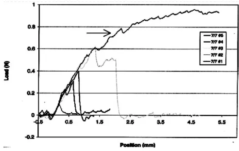
The bending tests revealed a large variation in the response of the joints, as shown in Fig. 8. This plot shows the load applied versus the deflection of the tube for tests at room temperature.
While most of the joints failed due to brittle fracture of the glass or silicon, the graph marked with an arrow represents a joint that did not. The failure mode of this sample was yielding of the tube, which eventually prevented any more load from being applied.
Fig. 9 is a plot of the failure strength of various joints in the baseline process as a function of the absolute test temper-ature and indicates the different failure mechanisms observed in these tests. As the temperature is increased, the strength de-creases, and the failure mechanism changes from fracture of the glass and silicon to yielding of the Kovar and the glass. At tem-peratures above 800 K, yielding of the glass became the cause of failure. The mean strength in bending at room temperature was 0.0115 Nm with a standard deviation of 0.0057 Nm, which corresponds to a nominal stress of in the Kovar tube. This value is close to the reported yield strength of Kovar (345 MPa [12]).
VI. TENSIONTESTS
Tension tests simulate the loads that a joint is expected to experience from high pressures in the tubes and during handling. To first order, the pressure in the tube can be related to the tensile load by the expression
Fig. 7. Bending test setup.
Fig. 8. Load-displacement response of several specimens in bending at room temperature. The specimens were manufactured using the baseline process.
Fig. 9. Moment applied at failure in bending tests is plotted against the test temperature for specimens prepared using the baseline process.
A. Experimental Details
Single-tube test specimens were prepared for tension tests by the use of EN-1 glass preforms to bond Kovar tubes to metal coated silicon in 800 air/35 propane atmosphere, without the
use of carbon fixtures. This manufacturing was performed by Vetro Fuse Inc. Two different metal films were used: 0.1 sputtered Kovar and e-beam evaporated bilayers of 0.5 Nickel/0.02 Ti. The silicon samples were prepared similar to the baseline process with the exception of an additional step that formed the thin metal layer. Following diesaw the samples were placed in a masking chuck, with circular holes, that formed annuli around the orifices, once the deposition was completed. The diameter of the deposited layers varied from 1.5 to 3.45 mm. (All other factors, such as the time of processing and the temperature of the furnace, were identical for all samples.)
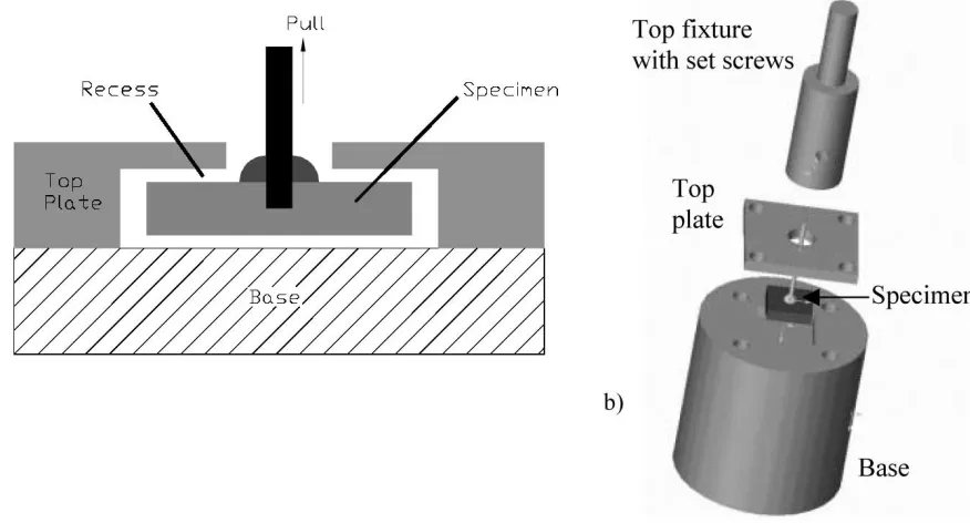
The specimens were placed in a fixture consisting of a base and top set screw designed to allow tension to be applied to the joint without the introduction of a moment (Fig. 10). The base of the fixture consisted of a recessed area to receive the silicon base; a drilled top plate is then lowered over the Kovar tube and attaches at four points around the recessed area. The Kovar tubes are then slipped into a corresponding axial hole in the top piece of the fixture, and a setscrew is tightened on the Kovar tube, allowing tension to be applied to the joint. To pre-vent shear stresses in the specimen the recessed area was de-signed to allow free movement of the device prior to loading, which began only after the silicon surface reached the top plate. Alignment was checked before each run and adjusted by moving the test sample on the steel block. The fixture was designed to fit on a servohydraulic mechanical testing machine. Testing con-sisted of subjecting the sample to a constant displacement rate of 10 at room temperature.
B. Results
[image:6.612.47.284.479.663.2]PELESet al.: FLUIDIC PACKAGING OF MICROENGINE AND MICROROCKET DEVICES 37
Fig. 10. Schematic illustration of the fixtures used for tension tests. (a) Cross section. (b) Isometric view. The top fixture is held stationary and the base is pulled down in a servohydraulic mechanical testing machine.
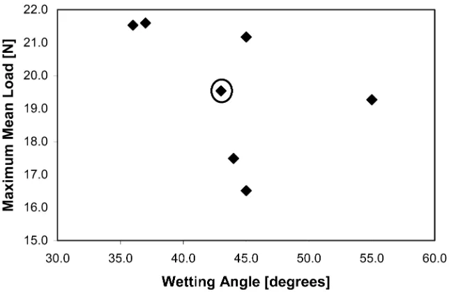
effect on the strength; in particular, the use of a coating does not degrade the strength compared to bare silicon. The locus of fracture is similar in all specimens, regardless of the presence or absence of any metal coating, and includes fracture in the glass, in silicon, and along the interfaces. This suggests that the adhesion strengths of silicon/glass, glass/metal, and metal/sil-icon are comparable. Further, as shown in Fig. 12, no correlation was found between the maximum sustained load and the wetting angle in these samples. However, the wetting angle alone does not determine the actual contact area since numerous voids are present at the glass/metal and glass/silicon interface.
Next, the maximum loads for one particular set (with Kovar coating of diameter 2.0 mm) were fit to a Weibull probability distribution [13]. The probability of failure, , is related to the applied load, , by the expression
(2) where is a reference load and is the Weibull modulus. By fitting the data to (2), the Weibull modulus was determined to be 5 and the reference load 20.1 N, as shown in Fig. 13. The coefficient of regression was 0.98, indicating a good fit.
[image:7.612.305.551.344.517.2]Fig. 13 has important implications for the design of single seals and for the reliability of packaged devices. Whereas the best performance among the tested specimens was a maximum load of , the low value of the Weibull modulus implies that only a significantly lower load can be applied to ensure a low probability of failure. Furthermore, a single packaged de-vice contains seals, with for the microrocket device; the failure of even one seal can cause the failure of the entire de-vice. These joints are spaced sufficiently apart that the fracture of any one seal is expected to be independent of the fracture of any other. Therefore, it follows that, if is the probability of survival of a single joint, then is the probability
Fig. 11. Maximum load sustained by single-tube specimens at room temperature (furnace atmosphere: 800 air/35 propane). For comparison, the mean strength of samples in the baseline process was 8.6 N.
of survival of the package. For operation pressures of 125 atm , Fig. 13 indicates that and the probability of survival of a package with eleven joints is 0.90. However, at pressures of 300 atm , and the probability of survival of the package is only . Even if , as in an alternate design, the probability of surviving 300 atm is still
.
It is important to note that these conclusions are valid only at room temperature. Similar tests at elevated temperatures, and under different loading conditions (especially bending), are nec-essary to map the entire operating space for these joints.
C. Fractography
Fig. 12. Maximum mean load as a function of the wetting angle. The bare silicon sample is circled. (Furnace atmosphere: 800 air/35 propane).
Fig. 13. Weibull plot for a set of 27 single-tube specimens tested in tension.
by the arrow is usually interpreted to be the result of crack prop-agation on parallel crystallographic planes [14]. This suggests that the crack propagates radially during the fracture process. Fig. 15 shows the tube and glass bead after fracture; a portion of the silicon substrate is seen on the top surface. A few tests were interrupted immediately following fracture initiation, as indicated by a drop in the load. Fig. 16 shows the top view of one such sample: it is clear that fracture proceeds by the acti-vation of multiple cracks, in the glass, in the silicon, and along the glass-silicon interface, in these specimens. Large voids are clearly visible in the glass.
In one specimen, the glass was dissolved using HF after processing, without subjecting the tube to tensile loads. No pre-cracks were observed in the substrate (Fig. 17).
VII. RESIDUALSTRESSES
[image:8.612.300.554.306.496.2]The results of Section VI show that, even with the process op-timized for small voids, good wetting and no pre-cracking, the
Fig. 14. Scanning electron micrograph of a fractured seal. The arrow marks the river pattern indicative of the outward propagation of the crack. Coated thin layer diameter— 1:5 mmKovar.
[image:8.612.310.550.548.726.2]PELESet al.: FLUIDIC PACKAGING OF MICROENGINE AND MICROROCKET DEVICES 39
Fig. 16. Scanning electron micrograph of a specimen whose testing was halted after fracture initiation. Coated thin layer diameter— 1:5 mmTi/Ni.
strength is insufficient for the full range of pressures required. To gain insight into the residual stress distribution, and to sug-gest methods for strength improvement, finite element calcula-tions were performed.
Processing-induced thermal residual stress result from a mismatch in the coefficients of thermal expansion . The glass and Kovar have closely matched values of of in the temperature range 20–700 [13], while the corresponding value for silicon is . The softening temperature of the glass is and it is reasonable to expect the glass to flow and accommodate all stresses until it reaches this temperature. Between 700 and room temperature, the differential contraction of the glass and silicon will induce stresses in both materials with a magnitude given, to first order, by
(3) where is the stress, is Young’s modulus, is Poisson’s ratio,
is the absolute softening temperature (973 K), and is the absolute room temperature (300 K). For typical values ( , ), (3) implies a maximum tensile stress of in the glass.
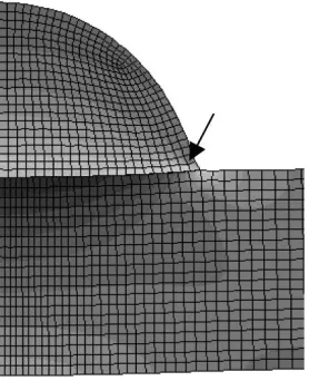
This analysis is valid only in regions away from the edges of the glass bead. The full stress field was determined using the method of finite elements. An axisymmetric model was created using a general-purpose code (ABAQUS/CAE, Hibbitt, Karlsson, and Sorensen, Inc.). Both materials were assumed to be isotropic, homogeneous, elastic solids, with
and . Any stress relief due to the presence of voids was ignored in the analysis; the predictions of the model are, therefore, worst-case estimates. As shown in Fig. 18, the stress field in the vicinity of the glass-silicon-air interface is complicated. The maximum tensile stresses in the glass of occur in the region indicated by the arrow in the figure, consistent with the locations of pre-cracks in Fig. 3.
[image:9.612.40.291.64.250.2]Even when the stress is insufficient to cause pre-cracks, as in Fig. 17, the residual stresses act as a pre-load, and lower
[image:9.612.360.499.277.448.2]Fig. 17. Scanning electron micrograph of the silicon surface after glass removal. Coated thin layer— 2 mmTi/Ni.
Fig. 18. Finite element mesh of a portion of the glass-silicon structure. The arrow indicates the location of maximum tensile stresses in the glass.
the strength in tension. Equation (3) suggests that the optimal strategy for minimizing residual stresses is to match the coef-ficients of thermal expansion of the metal and glass to silicon. Pyrex is an attractive candidate, although over a restricted tem-perature range (20 to 300 ). An alternate strategy is to choose glasses such that , rather than matched to either Kovar or silicon
VIII. CONCLUSION
The baseline process used in the glass sealing of Kovar tubes to silicon for making fluidic interconnects for high-tempera-ture, high-pressure operation was described. The effects of pro-cessing parameters on voiding and wetting behavior of the glass were qualitatively discussed, and experimental characterization of the strength of single-tube joints in bending and in tension was described. A numerical analysis of the residual stresses in glass-silicon composites was presented. Our main conclusions are as follows.
1) The volume fraction of voids within the glass is primarily dependent on the quality of the glass preform material. 2) The wetting behavior of glass on bare silicon is
However, this dependence can be negated by the use of metal-coated silicon substrate. Good wetting was consis-tently achieved using such samples in a variety of furnace conditions, obviating the need for carbon fixtures during processing.
3) Bending tests indicated that the mechanism of failure is fracture at room temperature and yielding of the Kovar and the glass at elevated temperatures.
4) The mean strength in tension at room temperature was not significantly affected by the presence of metal coatings. In addition, there was no apparent correlation between the strength and the wetting angle in the range of 35–55 . 5) For one set of 27 nominally identical samples tested in
tension at room temperature, the Weibull modulus was found to be 5 and the reference load 20.1 N. This implies that a packaged microrocket device with 11 equally crit-ical connections can survive 125 atm of pressure with a probability of 0.9. At 300 atm, however, the probability of survival of the package is unacceptably low . 6) Numerical analysis of the residual stresses indicate that the glass in the vicinity of the glass-silicon-air interface experiences the maximum tensile load, consistent with pre-crack patterns observed in several unstressed seals.
ACKNOWLEDGMENT
The authors gratefully acknowledge stimulating discussions with the members of the MIT Microengine Project, especially A. Epstein, H. Li, and M. Schmidt. They would also like to acknowledge G. Simpson from Vetro Fuse Inc., Pelham, NH for his sample furnace processing.
REFERENCES
[1] A. Epstein and S. D. Senturia, “Macro power from micro machines,” Science, vol. 276, p. 1211, 1997.
[2] A. P. London, A. A. Ayon, A. H. Epstein, S. M. Spearing, T. Harrison, Y. Peles, and J. L. Kerrebrock, “Microfabrication of a high pressure bipro-pellant rocket engine,”Sensors Actuators A, vol. 92, pp. 351–357, 2001. [3] B. L. Gray, D. Jaeggi, N. J. Mourlas, B. P. van Dreenhuizen, K. R. Williams, N. I. Maluf, and G. T. A. Kovacs, “Novel interconnection tech-nologies for integrated microfluidic systems,”Sensors Actuators A, vol. 77, pp. 57–65, 1999.
[4] C. Gonzalez, S. D. Collins, and R. L. Smith, “Fluidic interconnects for modular assembly of chemical systems,”Sensors Actuators B, vol. 49, pp. 40–45, 1998.
[5] E. Meng, S. Wu, and Y.-C. Tai, “Silicon couplers for microfluidic appli-cations,”Fresenius J. Anal. Chem., vol. 371, pp. 270–275, 2001. [6] T. S. Harrison, “Packaging of the MIT Microengine,” S.M., Mass. Inst.
Technol., Cambridge, MA, 2000.
[7] T. S. Harrison, A. P. London, and S. M. Spearing, “High-temperature, high-pressure fluid connections for power microsystems,” inMater. Res. Soc. Proc., vol. 654, 2001, paper EE6.5.
[8] Standard Specification for Iron-Nickel-Cobalt Sealing Alloy, F15-95, 1995.
[9] D. Y. Sim, T. Kurabayashi, and M. Esashi, “A bankable microvalve with a Kovar-glass-silicon-glass structure,”J. Micromech. Microeng., vol. 6, pp. 266–271, 1996.
[10] M. T. Blom, E. Chmela, J. G. E. Gardeniers, J. W. Berenschot, M. Elwen-spoek, R. Tijssen, and A. van den Berg, “Local anodic bonding of Kovar to Pyrex aimed at high-pressure, solvent-resistant microfluidic connec-tions,”J. Micromech. Microeng., vol. 11, pp. 382–385, 2001. [11] I. Kondo, O. Takenaka, T. Kamiya, Hayakawa, and A. Kinbara,
“Adhe-sion measurement of Ti thin films on Si substrate using internal stress in overcoated Ni films,”J. Vac. Sci. Technol. A, vol. 12, no. 1, pp. 169–173, Jan./Feb. 1994.
[12] [Online]. Available: www.hightempmetals.com/hitempKovardata.htm [13] B. Lawn,Fracture of Brittle Materials. Cambridge, U.K.: Cambridge
Univ. Press.
[14] G. E. Dieter,Mechanical Metallurgy. New York: McGraw-Hill, 1988.
Yoav Pelesreceived the Ph.D. degree in mechanical engineering from the Tech-nion—Israel Institute of Technology, Haifa, Israel, in 1999.
He joined the Massachusetts Institute of Technology Gas Turbine Laboratory, Cambridge, MA, to work with Prof. Alan H. Epstein, head of the gas turbine laboratory, and Prof. Martin A Schmidt, Director of the Microsystems Tech-nology Laboratory, for the Micro Rocket Project. He joined the department of the Mechanical, Aerospace and Nuclear Engineering at Rensselaer Polytechnic Institute, Troy, NY, as an Assistant Professor, in 2002. His main research focus is micro scale thermal-fluid.
V. T. Srikarreceived the B.Tech. degree in metallurgical engineering from Ba-naras Hindu University, Varanasi, India, and the Ph.D. degree in materials sci-ence from the Massachusetts Institute of Technology (MIT), Cambridge, MA, with a dissertation on the electromigration behavior and reliability of sub-mi-cron aluminum interconnects in silicon integrated circuits.
His postdoctoral research at MIT focused on the design, fabrication, and anal-ysis of micro- and nanoscale materials and structures and included studies of the shock reliability of MEMS, thermoelastic dissipation in polycrystalline mi-croresonators, and stress analysis using Raman spectroscopy. He was involved in the fluidic packaging of a microrocket device and the design of a microscale solid-oxide fuel cell.
Todd S. Harrisonreceived the S.B and S.M degrees in aeronautics and astro-nautics from the Massachusetts Institute of Technology (MIT), Cambridge, MA, in 1998 and 2000, respectively.
While a graduate student at MIT, he researched methods for making fluidic and electrical connections to high-temperature, high-pressure MEMS devices in support of the MIT micro-engine and micro-rocket projects. This research cul-minated in a thesis entitled “Packaging of the MIT Micro-Engine.” Following graduate school, he has worked for DiamondCluster International, Boston, MA, a management consulting firm, and AeroAstro, Boston, MA, a small aerospace company specializing in micro-satellite technologies. He is currently a Senior Consultant at Booz Allen Hamilton, McLean, VA, supporting the DOD’s satel-lite communications programs. He is also a Captain in the Air Force Reserves, where he serves as a Logistics Officer in the 42nd Aerial Port Squadron.
Christopher Protzwas born in 1977. He received the S.B and S.M. degrees in aeronautics and astronautics from the Massachusetts Institute of Technology (MIT), Cambridge, in 1998 and 2000, respectively. He is currently working to-ward the Ph.D. degree in the Gas Turbine Laboratory at MIT.
Anna Mracekis a Senior at the Massachusetts Institute of Technology (MIT), Cambridge, MA, in the Department of Aeronautics and Astronautics.
In addition to flight-related MEMS, she has worked on field testing Mars rover technology, developing structurally uniform metallic foams, and orbital debris. Other areas of involvement include the MIT Rocket Team and the MIT Chapters of the AIAA and SGT.
S. Mark Spearingreceived the Ph.D. degree from the Cambridge University Engineering Department, Cambridge, U.K., in 1990.
He worked as a Research Engineer at the University of California, Santa Barbara from 1990 to 1992, where he produced analytical models for the failure of high-temperature ceramic materials, and for carborundum micro-electronics, where he was a Member of the electronic packaging technology development team from 1992 to 1994. He is an Associate Professor of Aeronautics and Astronautics at the Massachusetts Institute of Technology (MIT), Cambridge, MA, where he has been since 1994. His technical interests include materials and structural analysis and design of MEMS, development of wafer bonding-technologies, microelectronic and MEMS packaging, and advanced composites. Since 1995, he has been responsible for materials, structural design and packaging tasks of the MIT MicroEngine, MicroRocket, Micro-Chemical Power and MicroHydraulic Transducer projects as well as conducting cross-cutting underpinning technology development.
Dr. Spearing is an Editor of the JOURNAL OFMICROELECTROMECHANICAL

![Fig. 6.�rocket [2] packaging scheme.](https://thumb-us.123doks.com/thumbv2/123dok_us/8519997.352785/5.612.75.516.65.186/fig-rocket-packaging-scheme.webp)