Int. J. Electrochem. Sci., 8 (2013) 3510- 3523
International Journal of
ELECTROCHEMICAL
SCIENCE
www.electrochemsci.org
Electrodeposition of In
2S
3Thin Films onto FTO Substrate from
DMSO Solution
B. Marí1
, M. Mollar1, D. Soro2, R.Henríquez3,*, R. Schrebler3, H. Gómez3 1
Departament de Física Aplicada-IDF, Universitat Politècnica de Vàlencia, Camí de Vera s/n, Vàlencia, 46022, Spain.
2
Université d’Abobo-Adjamé, UFR-SFA, 02 BP801 Abidjan, Côte d’Ivoire. 3
Instituto de Química, Facultad de Ciencias, Pontificia Universidad Católica de Valparaíso, Av. Universidad 330, Curauma Valparaíso, Chile.
*
E-mail: [email protected]
Received: 5 December 2012 / Accepted: 29 January 2013 / Published: 1 March 2013
In current work we report the electrochemical deposition of In2S3 thin films from a In(ClO4)3 and S8 in dimethylsulfoxide (DMSO) solution. Potenciodynamic experiments were conducted to study the electrochemical response of the precursors in the organic solvent. Chronoamperometric measurements allowed to establish the nucleation-growth mechanism of the indium sulfide phase and also to build a proper potential step program for achieving adherent good quality thin films. SEM micrographs exhibited complete substrate coverage whereas EDAX analysis gave In/S ratio very close to 2/3. Grazing XRD analysis showed that the films were grown in the tetragonal phase without the presence of oxide or hydroxide phases as usually is reported in aqueous medium. Results open the possibility of applying the procedure to the electrodeposition of an alternative In2S3 buffer layer onto copper indium diselenide substrates for evaluating the performance of the corresponding solar cell.
Keywords: In2S3, Buffer Layer, CIGS solar cells, Electrodeposition, DMSO.
1. INTRODUCTION
photovoltaic heterojunction are obtained with CdS manufactured by chemical bath deposition method (CBD). This method favors the n-CdS/p-CIS interface because offers a good coverage, low temperature deposition, chemical passivity and lack of the bombarding energetic species. However, the use of cadmium in PV devices is undesirable from the viewpoint of environmental safety [6] and serious efforts have been made to substitute the CdS buffer layer by other non-toxic low-absorbing materials.
In2S3 is one of the possible candidates to replace CdS as buffer layer. This compound is an n-type semiconductor that can be found under three polymorphic forms: a defect cubic -In2S3 structure under ambient conditions which changes to a defect spinel -In2S3 at 420°C and, to a layered structure -In2S3 at 740°C [7-9]. Depending upon the type and composition, the band gap reported for In2S3 compound varies between 2.0 and 2.45 eV [10]. Hetero-junctures as CIGS/-In2S3 [11] or CIS/In(OH,S) [12] have been built by CBD with conversion efficiencies of 15.7% and 11.4% respectively. This demonstrates that comparable conversion efficiencies can be obtained respect to commonly used CdS buffer (ca. 16% [13]). Atomic layer deposition [14], metal organic chemical vapor deposition [15] and ion layer gas reaction [16] have been also employed to form In2S3 thin layers onto CIS.
Electrodeposition, a widely used industrial process for large surface coating which has been successfully used to prepare semiconductor films, is another interesting alternative for In2S3 synthesis. The method allows the control of the bandgap width and the doping level through the control of variables such as solution composition, applied potential, pH and working temperature. Furthermore, monitoring the circulating charge it is also possible to control the thickness of the deposited layers. N.R. Tacconi et al. [17] employed the under-potential deposition of indium onto a sulfur-modified gold substrate to form an indium sulfide alloy. Through combined cyclic photovoltammetry and electrochemical quartz crystal microgravimetry scans, the authors demonstrate the growth of this film and its n-type characteristic. Later on, B. Asenjo et al. [18] carried out the electrochemical deposition of In2S3 thin films from an aqueous acid solution of In2(SO4)3 and Na2S2O3 onto Mo glass substrate. They demonstrated the one-step electrochemical deposition of -In2S3 films with good mechanical properties through reductive cyclic voltammetry. However, a secondary In2O3 phase appears on thinner films formed by parallel chemical precipitation or reduction with the dissolved oxygen during the first deposition stages, finally obtaining an In2S3 – In2O3 mixture. The authors justified the presence of this phase considering the electrochemical reduction of H+ and the chemical oxidation of In+. Both reactions produce a local pH increase close to the substrate surface, giving rise to chemical precipitation of indium oxides and hydroxides. Mixtures of oxide and hydroxide phases have been found when In2S3 is electrodeposited either onto Mo-coated, ITO-coated glass, CuInS2/Mo [19] or CIGSe substrates [20].
consecutive formation of a chalcogenide anion that further precipitates heterogeneously onto the surface of a convenient substrate for the formation of II-VI semiconductors [21, 22]. The same group employed a mixture of molecular oxygen and elementary S8, both dissolved in DMSO, to synthesize ZnO2–ZnS mixtures [23]. These were obtained at 100°C applying a potential that favored the combined reduction of both chalcogen precursors. The direct reduction of chalcogen precursor in elemental state can give: (i) an oxide phase without the presence of hydroxides that increase the band gap value of the film that acts as BL material and, (ii) films with a proper stoichiometry thanks to the slow mechanism of heterogeneous precipitation. The absence in the solution of chalcogen precursor in oxidation state VI also avoids the possible contamination by elementary chalcogen in the film.
In current work we report on the electrodeposition of In2S3 in DMSO solution employing indium perchlorate and elemental sulfur as precursors. After a previous voltammetric and chronoamperometric study a potential step potentiostatic program was designed to obtain adherent films with an appropriate stoichiometry. Besides, their optical and structural properties are in good agreement with those reported in the literature.
2. EXPERIMENTAL
3. RESULTS AND DISCUSSION. 3.1. Voltammetric study
-1.2 -0.8 -0.4 0.0
-4 -2 0 2
-4 -2 0 2 -1 0 1
E / V vs. Ag/AgCl
sat.j
/
m
A
c
m
-2
(c)
(b)
[image:4.596.172.411.131.514.2](a)
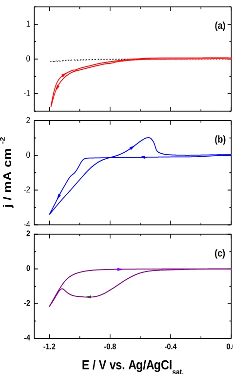
Figure 1. Potentio-dynamics responses of: a) (----) 10 mM KClO4 supporting electrolyte and () 50 mM S8 +10 mM KClO4, b) 40 mM In(ClO4)3 +10 mM KClO4 and c) 50 mM S8 + 40 mM In(ClO4)3 + 10 mM KClO4 system in DMSO solution. Cathodic and anodic scan rate employed 0.020 Vs1 and T = 70° C.
Figure 1 shows the first cycle of the potentiodynamic responses of the precursors, separately and mixed, involved in the indium sulfide electrodeposition. In Figure 1(a), no evident electrochemical processes associated with the supporting electrolyte can be seen in the potential interval considered. In presence of 50 mM S8, an small cathodic current starts at around 0.60 V followed by a progressive current increasing which extends to the end of the negative potential scan. The process is irreversible as no stripping peaks are observed in the reverse scan. According to the literature, the electrochemical reduction of S8 in organic solvents such as THF, DMF, DMSO or CH3CN onto different type of electrodes normally occurs in several electrochemical and chemicals steps [24]. The first one corresponds to the reduction of S8 to S82 followed by the formation of S8 x2
through successive steps [25-27]. The voltammetric response of In(ClO4)3 precursor is shown in the Fig. 1(b), where only the electrodeposition and further stripping of metallic indium -the latter process starting at 0.55 V- is observed.
When indium and sulfur precursors are present in solution (see Fig. 1(c)) the voltammetric response undergoes notorious changes. An intense and broad cathodic peak is developed in the potential region where the first step of S8 electroreduction takes place. Simultaneously, a brownish coloration is observed at the naked eye at the electrode surface, associated to indium sulfide formation through a reduction-precipitation process. The electrochemical and chemical reactions that can be proposed to explain the formation of the semiconductor phase are:
S8°(sol) + 2e– S82–(sol) (1)
3S82–(sol) + 2In3+(sol) In2S3(s) + 3S7 (2)
where the precipitation reaction (2) correspond to a special case proposed by A.S. Baransky et al. [28] for the formation of CdS from the electrochemical reduction of sulfur in DMSO solution. According to the precipitation theory, the formation of In2X3 type compounds (X= S, Se, Te) occurs when the over-saturation (S) reaches a critical value (S*) allowing the nucleation in solution (homogeneous precipitation). However, this process does not necessarily produce the formation of an attached film onto the substrate surface [29]. In contrast, at smaller S values but close to S*, the solution is in a meta-stable situation. Under these conditions, the precipitation of In2X3 phase can only be produced through pre-existent nucleation sites given by the substrate surface (heterogeneous precipitation) and this fact is consistent with the absence of a yellow coloration in the solution.
3.2. Chronoamperometric experiments
In order to perform a chronoamperometric study intended to analyze the nucleation-growth mechanism involved in the formation of the In2S3 phase, a potential interval (1.150 V Ed 1.050 V) was selected from the voltammetric results. Figure 2 exhibits the corresponding i/t transients evidencing that from Ed = 1.075 V (curve 2) appears a current contribution whose deconvolution is useful to give information about the different contributions involved in the nucleation and growth of a new phase on the FTO substrate. As the Ed value is made more negative, the i/t transients evolve towards successive current maximum. According to an early developed model, this kind of response can be attributed to a 2D nucleation and a layer by layer phase growing [30]. Instantaneous and progressive nucleation can be simultaneously distinguished by the model. The inset of Figure 2 shows the i/t transient obtained at 1.125 V which has been fitted with an equation that considers the following contributions:
1 2 3
T DL 2DI 2DI 2DP
where iDL corresponds to the double layer contribution and also to the reduction of sulfur to sulfide accompanied with the formation of the first In2S3 clusters on the substrate surface. i12DI represents the initial steps of the phase formation through an instantaneous 2D nucleation and growth mechanism (NGM).
0 25 50 75 100 125
0 1 2 3 4 4 3 2 1 5 4 3 1 i / m A
t / s
2
0 25 50 75 100 125
0 1 2 3 i / m A
t / s E
d = -1.125V
[image:6.596.166.424.173.383.2]Figure 2. i/t transients recorded in the 1.150 V Ed 1.050 V potential interval. The inset presents the deconvolution of the transient recorded at Ed = 1.125 V.
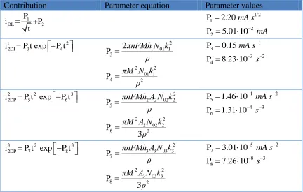
Table 1. NGM relationships for the different current contributions involved in Eq. (3)
Contribution Parameter equation Parameter values 1
DL 2
P
i = +P
t
1/2 1
P 2.20 mA s 2 2
P 5.01 10 mA
1 2
2DI 3 4
i = P t expP t 1 01 12
3 2
P πnFMh N k ρ
2 2
01 1
4 2
P πM N k ρ
1 3
P 0.15 mA s 3 2 4
P 8.23 10 s
2 2 3
2DP 5 6
i = P t expP t 2 2 02 22
5
P πnFMh A N k ρ
2 2
2 02 2
6 2
P
3
πM A N k
ρ
1 2
5
P 1.46 10 mA s 4 3 6
P 1.31 10 s
3 2 3
2DP 7 8
i = P t expP t 3 3 03 32 7
P πnFMh A N k ρ
2 2
3 03 3
8 2
P
3
πM A N k
ρ
5 2
7
P 3.01 10 mA s 8 3 8
[image:6.596.83.515.487.762.2]
Before the surface is completely covered with the first layer, a second contribution (i22DI), accounting for a bi-dimensional instantaneous nucleation is considered. According to this NGM model, the latter and the following contribution (i32DP) participates during the formation of the first and second layer. The NGM equations and the values of the corresponding parameters are presented in Table 1. These results are similar to those previously reported where the model was applied to the electrodeposition of Hg2Cl2 [31], Pd [32] and, more recently, Cu2O [33].
3.3. In2S3 electrodeposition
0 40 80 120 0
2 4 6
E
/
V
-1.15 V -0.6 V 0.4 V
60 s
120 s
(a)
i
/
m
A
t / s
0 40 80 120 t / s
60 s
120 s
(b)
t / s
cycle 2
[image:7.596.137.456.253.517.2]cycle 1
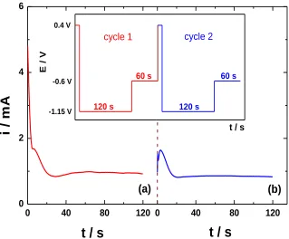
Figure 3.. i/t transients recorded during the application of the E/t perturbation program at Ed = 1.15 V. First (a) and second (b) cycles developed in a 10 mM KClO4 + 40 mM In(ClO4)3 + 50 mM S8 in DMSO onto FTO electrode. The working temperature was 70° C.
Taking into account the information provided by the analysis of the initial NGM steps, the electrodeposition of In2S3 films was performed selecting a potential perturbation program, which is included in the inset of Figure 3. The program consisted in the application of a first potential step from
4. FILMS CHARACTERIZATION 4.1. Structural study
20 30 40 50 60
(4
,1
,9
)
(1
,0
,1
5
)
(2
,2
,1
2
)
(0
,0
,1
2
)
In
te
n
s
it
y
/
a
.u
.
2 / degree
Incident angle= 0.5 deg Incident angle= 0.4 deg JCPDS #25-0390
(1
,1
,6
[image:8.596.153.438.135.402.2])
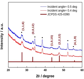
Figure 4. XRD pattern of electrodeposited In2S3 layers at 1.125V recorded under grazing incidence. Dots correspond to FTO substrate. Reference pattern JCPDS #25-0390 relates to a tetragonal structure. In this reference only XRD peaks with intensity higher than 15% have been plotted.
x
K D
cos
(4)
where K is a constant close to 1 (K = 0.9 was used), λx is the X-ray wavelength whose value is 1.54Å (CuKα), β is the full width at half maximum (FWHM) of the peak corrected by the instrumental broadening, while θ is the Bragg angle at the center of the peak. The crystallite size D obtained from this equation corresponds to the mean minimum dimension of a coherent diffraction domain. When determining the crystallite sizes, the (0,0,12) diffraction peak has been used, because is the strongest one in all the samples, what leads to less uncertainty in broadening determination. According to this procedure, a crystallite size of about 25 nm has been roughly calculated for In2S3 films by comparing the FWHM of its XRD peaks with that of FTO substrate.
4.2. Compositional and morphological characterization
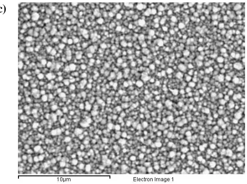
Scanning electron microscopy (SEM) has been employed to reveal the surface of the In2S3 thin films.
(a)
(c)
Figure 5. SEM micrographs for three typical In2S3 thin films electrochemically grown onto FTO substrates at: (a) –1.125 V, (b) –1.150 V and (c) –1.175 V respectively.
Figure 5 shows typical SEM surface morphologies for three different In2S3 thin films electrochemically obtained onto FTO substrates in a potential interval comprised between –1.125 V and –1.175 V. The images show a uniform morphology with crystallites of very small size which agrees with the analysis of grazing XRD patterns. The morphologic characteristics are independent of the electrochemical potential employed in the synthesis.
The reason lies in the nature of an electrochemical-precipitation process which involves the electrochemical reduction of indium ions to metallic indium, its corresponding striping and, further precipitation by reaction with the polysulfide ions formed from the electrochemical reduction of sulfur in DMSO solution. In fact, the morphological characteristic observed are entirely consistent with those obtained for In2S3 thin films formed in aqueous solution through of chemical bath deposition (CBD) [35,36]. Thus, all the samples show a cauliflower like morphology with aggregates that increase their size due to the increasing in the rate of the precipitation step as the potential is made more cathodic. The EDAX analysis shows an appropriate composition with an atomic ratio very close to the theoretical values (see Table 2). The decreasing in the atomic ratio at more cathodic potential indicates that the films present a small indium excess which is consistent with the voltammetric response observed for this precursor and the electrodeposition potential employed in the synthesis.
Table 2. Compositional characteristic obtained by EDAX for three different In2S3 thin films electrochemically grown at different electrodeposition potential.
Ed / V (120s)
%WIn %WS %At.In %At.S Experimental Atomic Ratio S/In
Theoretic values 70.48 29.52 40 60 1.50
1.125 69.47 30.53 38.56 61.44 1.59
1.150 69.41 30.59 39.21 60.78 1.55
[image:10.596.176.430.69.258.2] [image:10.596.74.522.660.751.2]
4.3. Optical characterization
250 500 750 1000
0 20 40 60 80 100
T
ra
n
s
m
it
ta
n
c
e
/
%
/ nm
(a)
1.5 2.0 2.5 3.0 3.5
0.0 0.5 1.0 1.5
(b)
(
h
)
2 /
e
V
2 m -2 x
1
0
14
h / eV
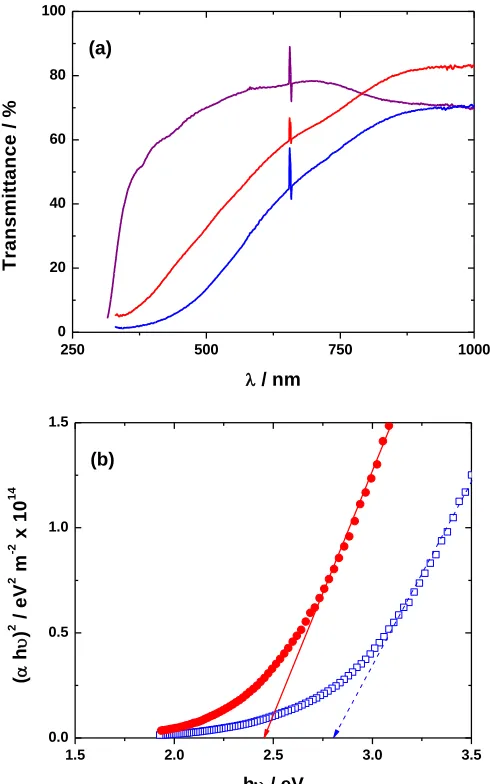
Figure 6. (a) Transmittance of a In2S3 thin film electrochemically formed onto FTO substrate at 1.125 V, the figure show the spectral response () as grown and () after a heat treatment at 450°C for 30 min, the () represent the optical response of FTO substrate. (b) Determination of bandgap energy through the (αhν)2
vs hν plot for the same sample () before and () after heat treatment.
The effect of the heat treatment in the optical transmittance in the visible region for a typical In2S3 thin film electrochemically grown at Ed = –1.125V is shown in Figure 6a. The transmittance grows with wavelength from 300 nm (about 0% transmittance) to approximately 875 nm. For wavelengths larger than 800 nm the transmittance remains almost constant at a net value (whole sample film+substrate) which is typically between 70% and 85%. Moreover, not evidence of oscillatory behavior caused by interference, whose origin can be either in In2S3 thin film or FTO substrate can be seen [37]. The absorption coefficient α was obtained from transmittance by
(1/ d) ln T
[image:11.596.164.409.108.500.2]
corresponds to the thickness of the deposit. A thickness of d = 890 nm can be estimated through the Faradic charge recorded for the two cycles employed in the synthesis. As In2S3 is a direct semiconductor it is expected that
h Eg
1/ 2 h [38, 39] where hν is the photon energy and Eg is the direct bandgap. The bandgap energy can be obtained by a linear fitting of
h
2 vs h plot [37]. Figure 6b shows a typical plot with the corresponding linear fitting before and after heat treatment. In both cases, it can be seen that the
h
2vs h plot follows an almost linear dependence above the bandgap value and is almost zero below this value. This zero value validates the approximation previously done neglecting the reflectance and dispersion. For the thin film obtained at Ed = –1.125V , the band gap energy values decreasing from 2.80 eV to 2.45 eV after the heat treatment which is very close to the accepted value [40]. As a general rule, the same behavior can be obtained independent of the electrodeposition potential employed in the synthesis. This indicates that the electrochemical reduction process of sulfur followed by the precipitation reaction (reactions (1) and (2) respectively) are consistent with the formation of In2S3 phases with similar morphological, optical and structural characteristics. The change in the band gap value can be correlated with possible nano-crystal sizes through the nano-crystal size effects, which agrees with the crystallite size found through the grazing XRD analysis.5. CONCLUSIONS
A detailed electrochemical study which included the voltammetric and chronoamperometric behavior of indium and sulfur precursors in DMSO solution allowed to find the best conditions for the electrodeposition of In2S3 thin films with adequate properties to be potentially used as alternative to CdS buffer layers in CIS based solar cells. XRD analysis showed that the films grown in the tetragonal phase without the presence of oxide or hydroxide phases which is consequence of using a non-aqueous solvent in the synthesis. SEM images revealed good substrate coverage and microstructure whereas EDAX analysis gave a stoichiometric composition very close to the expected. Optical measurements allowed to establish the band gap of the as grown as well as the annealed In2S3 films with values within those previously reported. Further work will be devoted to extend current results to the building of a CIS/In2S3 based solar cell and evaluation of its performance.
ACKNOWLEDGEMENTS
The authors acknowledge the support provided by FONDECYT Project No. 1090505 and the European Commission through Project NanoCIS (PIRSES-GA-2010-269279).
References
1. C.A. Kaufmann, A. Neisser, R. Klenk, R. Scheer, Thin Solid Films, 480-481 (2005) 515. 2. M.A. Contreras, B. Egaas, K. Ramanathan, J. Hiltner, A. Schwartzlander, F. Hasoon, R. Noufi,
3. T. Negami, Y. Hashimoto, S. Nishiwaki, Solar Energy Mater. Solar Cells, 67 (2001) 331. 4. Y. Hagiwara, T. Nakada, A. Kunioka, Solar Energy Mater. Solar Cells, 67 (2001) 267.
5. W. Fuhs and R. Klenk, Thin-film solar cells-overview, Proc. 2nd World Conf. and Exhibition on Photovoltaic Solar Energy Conv., 6–10 July (1998) 381, Vienna.
6. K.M. Hynes, J. Newham, Proceedings 16th European Photovoltaic Solar Energy Conference (2000) 2297.
7. J. M. Giles, H. Hatwell, G. Offergeld and J. Van Cakenberghe, J. Phys. Stat. Sol., 2 (1962) K73. 8. R. Diehl and R. Nitsche, J. Cryst. Growth, 28 (1975) 306.
9. C. D. Lockhande, A. Ennaoui, P. S. Patil, M. Giersig, K. Diesner, M. Muller and H. Tributsch, Thin Solid Films, 340 (1999) 18.
10. D. Hariskos, M. Ruckh, U. Rühle, T. Walter, H. W. Schock, J. Hedström and L. Stolt, Sol. Energy Mater. Sol. Cells, 41–41 (1996) 345.
11. D. Braunger, D. Hariskos, T. Walter, H.W. Shock, Material Solar Cells, 40 (1997) 97. 12. Kuveshni Govender, David S. Boyle and Paul O’Brien, J. Mater. Chem. 13 (2003) 2242. 13. W. Rehwald and G. Harbeke, J. Phys. Chem. Solids, 26 (1965) 1309.
14. A. Eicke, S. Spiering, A. Dresel, M. Powalla, Surf. and Interface Anal. 40 (2008) 830. 15. T.C. Deivaraj, M. Lin, K.P. Loh, M. Yeadon, J.J. Vittal, J. Mater. Chem., 13 (2005) 1149. 16. A. Belaidia, Th. Dittricha, D. Kievena, J. Tornowa, K. Schwarzburga, M. Kunsta, N. Allsopa,
M.Ch. Lux-Steinera, S. Gavrilovb, Solar Energy Mater. Solar Cells, 93 (2009) 1033. 17. N.R. de Tacconi, K. Rajeshwar, J. Electroanal. Chem, 444 (1998) 7.
18. B. Asenjo, A.M. Chaparro, M.T. Gutiérrez, J. Herrero, C. Maffiotte, Thin Solid Films, 480–481 (2005) 151.
19. T. Todorov, J. Carda, P. Escribano, A. Grimm, J. Klaer and R. Klenk, Sol. Energy Mater. Sol. Cells, 92 (2008) 1274.
20. N. Naghavi, E. Chassaing, M. Bouttemy, G. Rocha, G. Renou, E. Leite, A. Etcheberry and D. Lincot, Energy Procedia, 10 (2011) 155.
21. R. Henríquez, H. Gómez, G. Riveros, JF. Guillemoles, M. Froment and D. Lincot, Electrochem. Solid-State Letters, 7 (2004) C75.
22. R. Henríquez, H. Gómez, G. Riveros, JF. Guillemoles, M. Froment and D. Lincot, J. Phys. Chem. B. 108 (2004) 13191.
23. R. Henríquez, H. Gómez, P. Grez, D. Lincot , M. Froment, E.A. Dalchiele., G. Riveros; Electrochem. solid State Letters, 10 (2007) D134.
24. N.S.A. Manan, L. Aldous, Y. Alias, P. Murray, L. J. Yellowlees, M.C. Lagunas, and C. Hardacre, J. Phys. Chem. B, 115 (2011) 13873.
25. J. Lambling – Badoz, R. Bonaterre, G. Cauquis, M. Delamar and G. Demange, Electrochimica. Acta, 21 (1976) 119.
26. M. Delamar and J.C. Marchon, J. Electroanal. Chem., 63 (1975) 351.
27. R.P. Martin, W.H. Doubs, J.L. Roberts and D.T. Sawyer, Inorganic Chem., 12 (1973) 1921. 28. A.S. Baransky and W.R. Fawcett, J. Electrochem. Soc., 127 (1980) 766.
29. D. Lincot, MRS Bulletin, 35 (2010) 178.
30. A. Bewick, M. Fleischmann, H.R. Thirsk, Trans. Faraday Soc., 58 (1962) 2200.
31. I. Danaee, F. Shoghi, M. Dehghani Mobarake, M. Kameli, J. Solid State Electrochem., 14 (2010) 57.
32. S. Bijani, R. Schrebler, E.A. Dalchiele, M. Gabás, L. Martínez, and J. R. Ramos-Barrado, J. Phys. Chem. C, 115 (2011) 21373.
33. T.L. Barr, Y.L. Liu, J. Phys. Chem. Solids, 50 (1989) 657.
34. B.D. Cullity, Elements of X-ray Diffraction 2nd Ed. (Addi-son-Wesley, Reading, MA, 1978). 35. W. Vallejo, J. Clavijo, Brazilian Journal of Physics, 40 (2010) 30.
37. R. Henríquez, P. Grez, E. Muñoz, H. Gómez, J.A. Badán, R.E. Marotti, E.A. Dalchiele, Thin Solid Films, 518 (2010) 1774.
38. R. Yoosuf, M.K. Jayaraj, Sol Energy Mater Sol Cells, 89 (2005) 85.
39. R.E. Marotti, C.D. Bojorge, E. Broitman, H.R. Cánepa, J.A. Badán, E.A. Dalchiele, A.J. Gellman, Thin Solid Films, 517 (2008) 1077.