Manuscript received September 14, 2011; Revised January 09, 2012. Accepted for publication March 29, 2012.
Copyright © 2009 IEEE. Personal use of this material is permitted. However, permission to use this material for any other purposes must be obtained from the IEEE by sending a request to [email protected].
Seyed Behzad Naderi is with Department of Electrical Engineering, Sarab Branch, Islamic Azad University, 54716-376, Iran (email: [email protected]).
Mehdi Jafari is with Department of Electrical Engineering, Sarab Branch, Islamic Azad University, 54716-376, Iran (phone number: +98-914-886-6949, email: [email protected]).
Mehrdad Tarafdar Hagh is with Faculty of Electrical and Computer Engineering, University of Tabriz, 51666-16471, Iran (email: [email protected]).
Parallel Resonance Type Fault Current Limiter
Seyed Behzad Naderi, Student Member, IEEE, Mehdi Jafari, Student Member, IEEE, Mehrdad Tarafdar Hagh,
Member, IEEE
Abstract─This paper proposes a new parallel LC resonance type fault current limiter (FCL) that uses a resistor in series with the capacitor. The proposed FCL is capable to limit fault current magnitude near to pre-fault magnitude of distribution feeder current by placing the mentioned resistor in the structure of FCL. In this way, voltage of point of common coupling (PCC) does not experience considerable sag during the fault. In addition, the proposed FCL does not use superconducting inductor which has high construction cost. Analytical analysis for this structure is presented in detail and simulation results using PSCAD/EMTDC software are obtained to validate the effectiveness of this structure. Also, an experimental setup is provided to show the accuracy of analytic analyses and simulation results.
Index Terms─Parallel resonance, fault current limiter, resistor.
I. INTRODUCTION
Growth of power systems and their interconnections has resulted in increasing the short circuit currents level. The most common ways to limit high-level fault currents are: upgrading switchgear and other equipments, splitting the power grid, using higher voltage connections (ac or dc), using high-impedance transformers and etc. These alternatives may create other problems such as loss of power system safety, reliability, high cost and more power losses [1-4].
Fault current limiters (FCLs) are developed to overcome above-mentioned problems. An ideal FCL should have the following characteristics [5, 6]:
a) Zero impedance in the normal operation; b) No power loss in the normal operation; c) Large impedance in the fault conditions;
d) Quick appearance of impedance when the fault occurs; e) Fast recovery after fault removal.
The implementation of FCLs in electric power systems is not restricted to suppress the amplitudes of short circuit currents. They are also utilized to variety of performances such as power quality improvement, power system transient stability enhancement, reliability improvement and increasing
transfer capacity of system electrical energy. Therefore, an ideal FCL should have another important characteristic in addition to listed characteristics. It should play the load impedance role and be equal to load impedance during fault to better operation in such performances [7-11].
Different topologies for the FCL are introduced in literatures such as superconducting FCLs (SFCLs), solid state FCLs, flux-lock type FCLs and resonance type SFCLs [12-19]. Resonance type FCLs limit the fault current by using various topologies of series or parallel LC resonant circuits [18-23]. Series resonance type FCLs are composed of series connection of a capacitor and a superconducting inductor. They do not allow the short circuit current to increase instantaneously as the fault occurs. However, these FCLs can not limit the fault current level, if the fault continues. So, the fault current will increase continually [18, 19]. Because of using superconducting inductor, some of these structures need high construction cost. So, they are not commercially available, especially for third world countries. On the other hand, resonance type FCLs which do not use superconducting inductor and replace it with an ordinary copper coil, make power losses in their structures [20- 21].
Previously introduced parallel resonance type FCLs have used two anti-parallel semiconductor switches to make resonance condition between L and C. Operation of such structures results in large oscillations on the line current caused by LC resonance at first moments of the fault. These oscillations may harm system equipments [22, 23].
considerations for this FCL are presented and MATLAB software [24] is used to solve the resulted formulas. The circuit operation in the normal and fault conditions are simulated by using PSCAD/EMTDC software [25]. Experimental results in laboratory scale are presented, too.
II. POWER CIRCUIT TOPOLOGY AND PRINCIPLES OF OPERATION
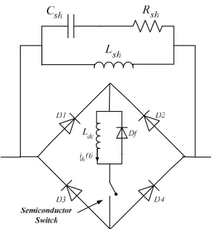
Fig. 1 shows single-phase power circuit topology of the proposed FCL. It is necessary to use a similar circuit for each phase in a three-phase distribution system. This structure is composed of two main parts which are as follows:
1) Bridge part: This part consists of a rectifier bridge containing D1 to D4 diodes, a small dc limiting reactor (Ldc),
a self turn off semiconductor switch (such as GTO, IGBT,etc.) and its snubber circuit and a freewheeling diode (Df ).
2) Resonance part: This part consists of a parallel LC resonance circuit (Lsh and Csh) (Its resonant frequency is equal
to power system frequency) and a resistor in series with the capacitor, Rsh.
Bridge part of the proposed FCL operates as a high speed switch that changes fault current path to the resonance part, when the fault occurs. Obviously, it is possible to substitute this part with an anti-parallel connection of two self turn off semiconductor switches [22, 23]. Using a diode rectifier bridge has two advantages compared to two anti-parallel switches as follows:
1) This structure uses only one controllable semiconductor switch which operates in dc side instead of two switches that operate in ac side. The control circuit is simpler because of no need for ON/OFF switching in the normal operation case.
2) It is possible to use a small reactor in series with the semiconductor switch at dc side. This reactor plays two roles as follows:
(a) It is snubber for semiconductor switch;
(b) It is as a current limiter at first moments of fault occurrence.
Figure 1. Single-phase power circuit topology of the proposed parallel resonance type FCL
However, placing dc reactor inside the bridge makes voltage drop on it because of dc current ripple. But, the current ripple is low and consequently voltage drop caused by it is not considerable in comparison with the feeder’s voltage. Current ripple and voltage drop equations are studied completely in [6] and [26].
It is important to note that high rating semiconductor switches are commercially available with current rating up to 24kA and voltage rating up to 4kV [27]. Also, it is possible to use some series and/or parallel self turn off switches considering high current and voltage levels. The semiconductor switch needs suitable snubber circuit for its protection which is not shown in Fig. 1 for simplicity. Also, high rating semiconductor switches, their protection procedure and minimization of their power losses are discussed in [28- 32].
From power loss point of view, in the normal condition, the proposed FCL has the losses on the rectifier bridge diodes, the semiconductor switch and small resistance of dc reactor. Each diode of the rectifier bridge is ON in half a cycle, while semiconductor switch is always ON. Therefore, the power losses of this FCL in the normal operation can be calculated as Eq. (1).
2
. 4
loss R D SW dc dc DF ave SWF dc
P =P +P +P =R I + V I +V I (1)
where:
Idc: dc side current which is equal to peak of line current
(Ipeak);
Rdc: Resistance of dc reactor
VDF : Forward voltage drop on each diode;
VSWF : Forward voltage drop on the semiconductor switch;
Iave. : Average of diodes current in each cycle that is equal to
peak
I π .
[image:2.612.93.246.505.671.2]Considering Eq. (1) and the small value of dc reactor in this structure, total power losses of the proposed structure becomes a very small percentage of the feeder’s transmitted power.
Fig. 2 shows the control circuit of the proposed FCL. In the normal operation of the power system, the semiconductor switch is ON. So, Ldcis charged to peak of the line current and
behaves as a short circuit. Using semiconductor devices (diodes and semiconductor switch) and small dc reactor, cause a negligible voltage drop on the FCL.
When a fault occurs, dc current becomes greater than the maximum permissible current I0 and the control circuit detects
it and turns the semiconductor switch off. So, the bridge retreats from utility. At this moment, freewheeling diode Df,
turns on and provides free path for discharging the dc reactor. When the bridge turns off, fault current passes through the parallel resonance part of FCL. Consequently, large impedance enters to the circuit and prevents rising the fault current. In the fault condition, parallel LC circuit starts to resonance. In this case, because of resonance, the line current oscillates with large magnitude [22, 23]. These oscillations may lead to damage system equipments or put them in stress. But, by placing a resistor (Rsh) in series with the capacitor,
current transients damp quickly that will be shown in simulations section. In addition, by using Rsh, voltage drop on
Figure 2. Control circuit of the proposed FCL
When the fault is disappeared, while semiconductor switch is OFF, parallel part of FCL will be connected in series with the load impedance. Therefore, line current will be decreased, instantaneously. To detect this instantaneous reduction of line current, iL is compared with (If) that can be calculated from
Eq. (2).
PCC f
eq V I
Z
= (2)
where, Zeq is the equivalent impedance of resonance part.
When the difference of iiLL andIf become greater than k as the
fault removal sign, the control circuit turns the semiconductor switch ON. So, power system returns to the normal state. The value of k can be calculated from Eq. (3) as follow:
,min
PCC PCC
eq eq L
V V
k
Z Z Z
= −
+ (3)
where, ZL,min is the minimum impedance of load on the
protected feeder.
As pointed, some of previously proposed FCL structures have ac power losses at resonant circuit in the normal condition, because of placing large inductor in the line current path [20, 21]. But, the proposed structure in this paper has very low losses in the normal condition, because the inductor is bypassed by the bridge part. Also, by choosing proper values for resonant circuit, the proposed FCL limits the fault current in a way that power system is not affected by the fault. In such condition, there will not be any considerable voltage sag on PCC voltage.
III. ANALYTICAL ANALYSIS
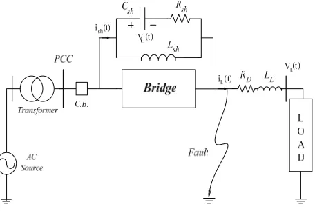
Fig. 3 shows the single line diagram of power system including the proposed FCL. This figure is composed of power source, transformer, circuit breaker (C.B.), FCL, line impedance and load. The circuit breaker (C.B.) which is rated for the full system short circuit current is placed to ensure the adequate protection of power system during permanent faults. The utility voltage is a three-phase sinusoidal waveform. The utility side impedance is modeled by series connection of a resistor Rs and an inductorLs.
Analytical analysis is discussed in two modes as follows:
Figure 3. Single line diagram of power system
Time
Li
ne cu
rr
en
t
tftsw
[image:3.612.74.277.57.157.2]Mode 1 Mode 2
Figure 4. Enlarged view of line current before and after fault
Mode 1: Pre-fault steady state operation (until tf in Fig. 4). Mode 2: Between fault occurrence and fault removal (from
f
t to fault removal time in Fig. 4).
A. Mode 1
In the normal operation of power system, the bridge part bypasses the resonant circuit. In this condition, the line current (iL) can be expressed by differential equation (4):
(
)
sin( )
s L L
V ωt = Ri +ωL di d tω (4)
where:
: s
V Peak of utility voltage
ω: Angular frequency of utility voltage
s L D
R R= +R +R (Resistance of source side, load and distribution feeder, respectively)
s L D
L L= +L +L (Inductance of source side, load and distribution feeder, respectively)
So, the line current equation can be derived as follow:
( )
2 2 2 2 2 2
( ) ( )[( ) R L t sin( )]
L s
[image:3.612.334.550.258.361.2]where:
arctan( L R)
ϕ= ω (6)
B. Mode 2
When a short circuit occurs, the dc limiting reactor can limit the increasing rate of fault current. The semiconductor switch doesn’t operate until the line current reaches to a pre-defined value. By semiconductor switch operation in tswinstant (Fig. 4), the bridge is switched off and the fault current is suppressed by resonant circuit. So, differential equation of fault current can be expressed as follow:
(
)
(
)
(
)
3 3 2 2 2 ( ) ( )( )sin( ) cos( )
s sh sh L
s sh sh s sh sh sh sh sh L
s sh sh s sh L s L
s sh sh sh sh s
L L C d i dt
R L C L R C R L C d i dt
L R C R L di dt R i
V L C ω ωt R C Vω ωt
⎧ ⎪ ⎪+ + + ⎪ ⎨ ⎪+ + + + = ⎪ ⎪ − + ⎩ (7)
with initial values as follows:
(
)
(
)
(
)
(
)
(
)
(
)
(
)
0 0 2 2 2 0 0 ( )( ) ( sin( ) ( ))
( ) ( cos( )
1
( sin( ) ( ) ( ))
L sw
L sw s sw s sh s
L sw s sw
sh sh sh
s sw s sh s sh s
i t t I
di dt t t V t I R R L
d i dt t t V t
I R L C
V t I R R L R R
ω ω ω ω ⎧ ⎪ = = ⎪ = = − + ⎪ ⎪⎪ = = ⎨ ⎪ ⎪+ − ⎪ ⎪− − + + ⎪⎩ (8) where: 0
I : Pre-defined line current for semiconductor switch operation.
Eq. (7) is solved by MATLAB software and its results are presented in simulations section in detail. After damping transients, the fault current equation can be expressed by Eq. (9).
cos( ) sin( )
L
i =A ωt +B ωt (9)
where:
2 2 3
3 2 2 2
( ) (1 )( )
( ) ( )
s sh sh sh sh
V R C d b L C c a
A
c a d b
ω ω ω ω ω
ω ω ω
⎡ ′− ′ − − ′ − ′ ⎤
⎣ ⎦
=
′ − ′ + ′ ′−
3 2 2
3 2 2 2
( ) (1 )( )
( ) ( )
s sh sh sh sh
V R C a c L C d b
B
c a d b
ω ω ω ω ω
ω ω ω
⎡ ′ − ′ − − ′− ′ ⎤
⎣ ⎦
=
′ − ′ + ′− ′
s sh sh
a′ =L L C ,
s sh sh s sh sh sh sh sh
b′ =R L C +L R C +R L C ,
s sh sh s sh
c′ =L +R C R +L ,
s
d′ =R (10)
By considering Eq. (9) and choosing proper values for Lsh,
Csh and Rsh, it is possible to limit the line current in the fault
condition in a way that its value to be near to the pre-fault line current. In this case, if the fault occurs, PCC voltage will not sense the fault.
IV. DESIGN CONSIDERATIONS
As discussed in section 2, Ldc is used to limit increasing
speed of fault current and help the semiconductor switch to turn off in a safe condition. So, its value can be chosen by considering current characteristics of semiconductor switch.
For resonant circuit design, two main cases should be taken into account: first, equating resonance part equivalent impedance with load impedance; second, generated heat in resistor of resonance part during fault and its design problem. Equivalent impedance of resonance part, Zeq can be derived as
follow:
( ) sh
eq sh sh sh
sh sh sh
L j
Z = R − ωC j Lω = C R + j Lω (11)
For equating this impedance with load impedance, Lsh
should be equal to load inductance. Corresponding capacitor value, Csh can be calculated considering resonance condition
between it and Lsh. Finally, resistor value should be chosen in
a way that Lsh/CshRsh be equal to load resistance. But, it is
difficult to equate these impedances exactly and it is ideal case because of load variation on distribution feeders. From practical point of view, parameters of resonance part can be determined by using the history of measurements of load at protected feeder and discussed calculations.
Following discussion deals with the operation of the proposed structure in practical condition. Fig. 5 shows the magnitude of voltage deviation of PCC of test system from its base value (that is the pre-fault voltage magnitude of PCC). The horizontal axis of this figure shows the magnitude of impedance of load in per-unit where the base value is its impedance of ideal case. The dashed line shows the existence of ideal case. The parameter of this figure is the magnitude of source impedance. This figure shows that for a wide range of load magnitude variations (0.5 to 2 p.u. with fixed resonance part parameters), the voltage magnitude of PCC for post-fault condition changes in an acceptable range especially for low values of |Zs|.
For considering the generated heat in resistance of resonance part, it is possible to change the values of Lsh, Csh
and Rsh and decrease the real part of Eq. (11). Note that the
magnitude of Zeq should be kept constant. Fig. 6 shows the
fault current magnitude respect to Rsh. Parameter of this figure
transient response of resonant circuit. Standard values for Csh
are obtained from [33] and Lsh is calculated by considering
resonance condition between it and Csh in power frequency. As a numerical example, it is considered that feeder’s average current is 256A. In this condition, pre-desired value of fault current (256A) can be achieved by two values for resonant circuit parameters as follows:
Case 1: Csh =150 Fμ ,Lsh =68mH,Rsh = Ω16
Case 2: Csh =107 Fμ ,Lsh =95mH,Rsh =49Ω
|Zeq| in cases 1 and 2 are equal. However, in case (2), real
part of Zeq is smaller than its value in case (1). So, generated
heat in Rsh is reduced in fault condition. As a result, design of
[image:5.612.61.273.255.417.2]Rsh becomes simpler from thermal point of view.
Figure 5. Voltage magnitude of PCC when equivalent impedance of resonance part is not equal to protected feeder load impedance (non-ideal
[image:5.612.57.286.486.661.2]case).
Figure 6. Variation of fault current magnitude respect to Rsh
V. SIMULATION RESULTS
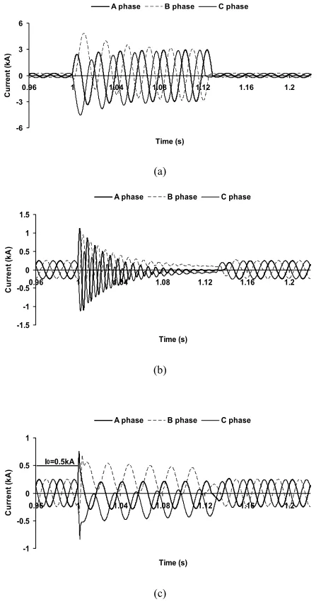
The power circuit topology of Fig. 3 is used for simulation in the fault condition. Simulation parameters are shown in Table I. Fault starts at 1s and continues to 1.12s (6 cycles of power frequency).
Simulation results for line current are shown in Fig. 7. Note that the current scales of figures are selected different to show more details. As fault occurs, without using FCL, fault current increases extremely and has asymmetrical nature (Fig. 7a). Also, without using Rsh in resonant circuit, transient
oscillations appear on the line current caused by LC resonance as shown in Fig. 7b. After damping of these transients, line current becomes a small value near to zero. Fig. 7c shows the line current in the fault condition by using the proposed resonance type FCL. As shown in Fig. 7c, when fault current reaches to I0 that is the pre-defined fault level, semiconductor
switch turns off and line current is limited in the fault condition. After fault removal, the semiconductor switch turns on and line current returns to the normal state, after negligible distortion. Although the proposed FCL can limit the fault current, this current magnitude can vary according to Fig. 7c. Therefore, it is necessary to set the secondary switching device for full short circuit current of power system.
Fig. 8 shows dc reactor current. As the fault occurs, it starts to charge until semiconductor switch turning off. After semiconductor switch turning off, the freewheeling diode turns on and discharges Ldc. After fault removal, Ldc recharges
because of resonant circuit voltage. By discharging resonant circuit, dc reactor current discharges and returns to the normal state.
Current of resonance part during the fault, i tsh( ) for A phase is shown in Fig. 9. It is obvious that after semiconductor switch operation, line current will be equal to resonance part current. Fig. 10 shows the PCC voltage with and without using the proposed structure. As shown in this figure, the proposed FCL can prevent voltage sag on PCC, properly. Also, the PCC voltage without using Rsh in the proposed FCL is
shown in Fig. 11.
It is observed that undesired distortions appear on the PCC voltage caused by the resonance current. The capacitor voltage is shown in Fig. 12.
TABLE I. SIMULATION SYSTEM PARAMETERS
Power source 20 kV, 50Hz, 0.57 0.003 source
Z = +jω Ω
Source Side Data
Transformer 20 kV/6.6 kV, 10 MVA, 0.1 p.u.
dc side Ldc= 0.01 H,
DF SW 0
V =3V, V =3V, I =0.5kA FCL Data
Resonance part
sh
L = 0.068 H, Csh=150 Fμ sh
R = 16 Ω
To demonstrate the accuracy of calculations, differential equation (7) that shows the line current during fault, is solved by MATLAB software and its result is shown in Fig. 13. This figure is in good agreement with Fig. 7c. The peak value of current in both figures (Fig. 7c and 13) is 256A. Values and variation of curve show that results of calculations are adapted by simulation result of PSCAD/EMTDC software. This can prove the correction of Eq. (7) to (10).
-6 -3 0 3 6
0.96 1 1.04 1.08 1.12 1.16 1.2
Time (s)
C
u
rr
e
n
t (k
A
)
A phase B phase C phase
(a)
-1.5 -1 -0.5 0 0.5 1 1.5
0.96 1 1.04 1.08 1.12 1.16 1.2
Time (s)
C
u
rr
e
n
t (k
A
)
A phase B phase C phase
(b)
-1 -0.5 0 0.5 1
0.96 1 1.04 1.08 1.12 1.16 1.2
Time (s)
C
u
rr
e
n
t (k
A
)
A phase B phase C phase
I0=0.5kA
(c)
Figure 7. Fault current ( )i tL , (a) without FCL (b) without Rsh in resonance type FCL (c) with the proposed FCL
-1 -0.5 0 0.5 1
0.96 1 1.04 1.08 1.12 1.16 1.2
Time (s)
Cu
rr
e
n
t (
k
[image:6.612.53.558.72.657.2]A)
Figure 8. dc reactor current, i tdc( ) for A phase
-0.8 -0.4 0 0.4 0.8
0.96 1 1.04 1.08 1.12 1.16 1.2
Time (s)
C
u
rr
e
n
t (k
A
)
Figure 9. Resonance part current during the fault, i tsh( ) for A phase
-15 -10 -5 0 5 10 15
0.96 1 1.04 1.08 1.12 1.16 1.2
Time (s)
Vo
lt
ag
e
(k
V
)
Without FCL With FCL
Figure 10. PCC voltage of A phase without (▬) and with (----) the proposed FCL
-20 -10 0 10 20
0.96 1 1.04 1.08 1.12 1.16 1.2
Time (s)
Vo
lt
a
g
e (
k
V)
[image:6.612.58.285.160.590.2]-10 -5 0 5 10
0.96 1 1.04 1.08 1.12 1.16 1.2
Time (s)
Volta
g
e (kV
)
Figure 12. Capacitor voltage, V tC( ) for A phase
Figure 13. Calculated fault current, ( )i tL by MATLAB software To study the non-ideal case which is discussed in section 4, the load is changed to 0.5p.u. in simulation system and its results are presented in Figs. 14 and 15. Fig. 14 shows the line current (A phase) for non-ideal case. As shown in this figure, the line current is smaller than its value during fault. The PCC voltage in such condition is shown in Fig. 15. According to this figure, small voltage sag appears in PCC. This voltage sag is predictable considering Fig. 5 in the section 4.
To determine the rating of FCL components, it is possible to use simulation results as well as the design considerations mentioned in section 4. Of course, for all semiconductor devices, maximum on-state current is the peak of line current. The maximum off-state voltage for these devices is the PCC voltage during the fault. The current rating of Ldc is the peak
of line current. Also, the resonance part inductance, Lsh will
appear during the fault. Therefore, in the worst condition, its voltage will be PCC voltage. So, its current rating can be determined. For the capacitor Csh, simple voltage dividing
method can be used between it and the resistor Rsh.
-0.6 -0.3 0 0.3 0.6
0.96 1 1.04 1.08 1.12 1.16 1.2
Time (s)
C
u
rre
n
t (k
A
)
Figure 14. Line current of A phase in non-ideal case (A phase)
-10 -5 0 5 10
0.96 1 1.04 1.08 1.12 1.16 1.2
Time (s)
V
o
lt
age (
k
V)
Figure 15. PCC voltage of A phase during the fault in non-ideal case
VI. EXPERIMENTAL SETUP
The performance of proposed FCL is experimentally investigated using a laboratory scale power system simulator. The power system for experimental study is as Fig. 3. Note that the control circuit of the proposed FCL is implemented by software. Experimental setup parameters and control circuit data are presented in Table II. According to the available elements values in market and experimental setup facilities, the components values in experimental setup are selected as much as possible near to simulation values which were obtain by the proposed design procedure. Fig. 16 shows the line current by using the proposed FCL. This figure is in good agreement with Fig. 7c. Resonance part current during fault is shown in Fig. 17.
PCC voltage without using the proposed FCL is shown in Fig. 18. It is observed that PCC voltage drops strongly. Using the proposed FCL prevents this voltage sag as shown in Fig. 19. In such condition, a negligible distortion appears on PCC voltage at fault occurrence instant. Notice that the time scale in Fig. 19 is magnified to emphases on small distortion of voltage in fault instant. Fig. 18 and 19 are in accordance with Fig. 10. Fig. 20 shows the capacitor voltage in fault condition. It is in agreement with Fig. 12.
TABLE II. EXPERIMENTAL SYSTEM PARAMETERS
Power source 220 V(peak), 50Hz, 0.5 0.005 source
Z = +jω Ω
Source Side Data
Transformer 220 V/110V, 10 kVA, 0.1 p.u.
dc side Ldc= 0.01 H,
DF SW 0
V =1V, V =1V, I =8A Resonance
part
sh
L = 0.07 H, Csh=150 Fμ sh
R = 15 Ω FCL Data
Control circuit
Current sensor: CSNE151-100 Gate driver: IR2113 Microcontroller: ATMEGA32 Switch: GW40NC60V
[image:7.612.62.278.59.150.2] [image:7.612.330.547.60.156.2] [image:7.612.64.273.210.312.2] [image:7.612.63.276.587.681.2]Figure 16. Line current by using the proposed FCL, (Amper/Div.: 5A, Time/Div. : 25 ms)
Figure 17. Current of resonance part during fault, (Amper/Div.: 5A, Time/Div.: 25 ms)
Figure 18. PCC voltage without using FCL, (Volt/Div.: 50V, Time/Div. 25 ms)
Figure 19. PCC voltage by proposed FCL, (Volt/Div.: 50V, Time/Div.: 10ms)
Figure 20. Capacitor voltage during fault, (Volt/Div.: 50V, Time/Div.: 25ms)
VII. CONCLUSION
In this paper, a new topology of parallel LC resonance type fault current limiter that includes a series resistor with the capacitor of LC circuit is introduced. The analytical analysis and design considerations for this structure are presented. The overall operation of mentioned FCL in normal and fault conditions are studied in detail. Also, simulation and experimental results are involved to validate analytic analyses. All early proposed FCLs have good current limiting characteristics. However, as shown in this paper, the proposed structure can improve power quality of distribution system in addition to fault current limiting. Proposed resonance type FCL can limit fault current in a way that PCC voltage does not face considerable sag during fault. This means that, in case of transient faults, it is not necessary to open the line by circuit breaker. By using Rsh in the proposed topology, transient state after fault damps quickly. In addition, it is capable of controlling fault current at constant value that is not possible in common series resonance type FCLs.
REFERENCES
[1] M. Jafari, S. B. Naderi, M. Tarafdar Hagh, M. Abapour and S. H. Hosseini, “Voltage sag compensation of point of common coupling (PCC) using fault current limiter,” IEEE Trans. Power Del., vol. 26, no. 4, pp. 2638-2646, Oct. 2011.
[2] S. P. Valsan and K. Sh. Swarup, “High-speed fault classification in power lines: theory and FPGA-based implementation,” IEEE Trans. Ind. Electron., vol. 56, no. 5, pp. 1793−1800, May 2009.
[3] P. Rodriguez, A. V. Timbus, R. Teodorescu, M. Liserre and F. Blaabjerg, “Flexible active power control of distributed power generation systems during grid faults,” IEEE Trans. Ind. Electron., vol. 54, no. 5, pp. 2583−2592, Oct. 2007.
[4] M. F. Firuzabad, F. Aminifar and I. Rahmati, “Reliability study of HV substations equipped with the fault current limiter,” IEEE Trans. Power Del., vol. 27, no. 2, pp. 610-617, Apr. 2012.
[5] A.Y. Wu and Y. Yin, “Fault-current limiter applications in medium- and high-voltage power distribution systems,” IEEE Trans. Ind. Electron., vol. 34, no. 1, pp. 236−242, Jan./Feb. 1998.
[6] M. Tarafdar Hagh and M. Abapour. “Non-superconducting fault current limiters,” Euro. Trans. Power Electron., vol. 19, Issue 5, pp. 669–682, Jul. 2009.
[7] M. Tarafdar Hagh, M. Jafari and S. B. Naderi, “Transient stability improvement using non-superconducting fault current limiter,” in Proc. IEEE 1st Power Electronic & Drive Systems & Technologies Conf.,
Feb. 2010, pp. 367-370.
[8] S. H. Hosseini, M. Tarafdar Hagh, M. Jafari, S. B. Naderi and S. Gassemzadeh, “Power quality improvement using a new structure of Fault instant
[image:8.612.65.278.53.161.2] [image:8.612.335.547.54.160.2] [image:8.612.65.279.216.325.2] [image:8.612.66.278.380.488.2] [image:8.612.64.282.543.651.2]fault current limiter,” in Proc. IEEE International Electrical Engineering Conf. (ECTI_CON), May 2010, pp. 641-645.
[9] A. Gyore, S. Semperger, L. Farkas and I. Vajda, “Improvement of functionality and reliability by inductive HTS fault current limiter units,” IEEE Trans. Appl. Supercond., vol. 15, no. 2, pp. 2086-2089, Jun. 2005.
[10] Yu-Hsing Chen, Chang-Yi Lin, Jhao-Ming Chen, and Po-Tai Cheng, “An inrush mitigation technique of load transformers for the series voltage sag compensator,” IEEE Trans. Power Electron., vol. 25, no. 8, pp. 2211-2221, Aug. 2010.
[11] Po-Tai Cheng, Wei-Ting Chen, Yu-Hsing Chen, Chia-Long Ni, and Jarsun Lin, “A transformer inrush mitigation method for series voltage sag compensators,” IEEE Trans. Power Electron., vol. 22, no. 5, pp. 1890-1899, Sep. 2007.
[12] Ohsaki H., Sekino M. and Nonaka S., “Characteristics of resistive fault current limiting elements using YBCO superconducting thin film with meander-shaped metal layer,” IEEE Trans. Appl. Supercond., vol. 19, no. 3, pp. 1818-1822, Jun. 2009.
[13] Sung-Hun Lim, Hyo-Sang Choi, Dong-Chul Chung, Yeong-Ho Jeong, Yong-Huei Han, Tae-Hyun Sung and Byoung-Sung Han, “Fault current limiting characteristics of resistive type SFCL using a transformer,” IEEE Trans. Appl. Supercond., vol. 15, no. 2, pp. 2055-2058, Jun. 2005.
[14] B. Ch. Sung, D. K. Park, J. W. Park and T. K. Ko, “Study on a series resistive SFCL to improve power system transient stability: modeling, simulation and experimental verification,” IEEE Trans. Ind. Electron.,
vol. 56, no. 7, pp. 2412−2419, Jul. 2009.
[15] M. Abapour and M. Tarafdar Hagh. “Non-superconducting fault current limiter with controlling the magnitudes of fault currents,” IEEE Trans. Power Elec., vol. 24, no. 3, pp. 613-619, Mar. 2009.
[16] Hyo-Sang Choi, Na-Young Lee, Young-Hee Han, Tae-Hyun Sung, and Byoung-Sung Han, “The characteristic analysis between flux-coupling and flux-lock type SFCL according to variations of turn ratios,” IEEE Trans. Appl. Supercond., vol. 18, no. 2, Jun. 2008.
[17] M. T. Hagh, S. B. Naderi and M. Jafari, “New resonance type fault current limiter,” in Proc. IEEE International Conference on Power and Energy (PECon), Nov./Dec. 2010, pp. 507-511.
[18] K. Arai, H. Tanaka and M. Inaba, “Test of resonance-type superconducting fault current limiter,” IEEE Trans. Appl. Supercond., vol. 16, no. 2, pp. 650-653, Jun. 2006.
[19] H. Arai, M. Inaba and T. Ishigohka, “Fundamental characteristics of superconducting fault current limiter using LC resonance circuit,”
IEEE Trans. Appl. Supercond., vol. 16, no. 2, pp. 642-645, Jun. 2006. [20] Hector G. Sarmiento, “A fault current limiter based on an LC resonant
circuit: design, scale model and prototype field tests,” in Proc. iREP Symposium-Bulk Power System Dynamics and Control-VII, Revitalizing Operational Reliability, Aug. 2007, pp. 1-5.
[21] S. Henry and T. Baldwin, “Improvement of power quality by means of fault current limitation,” in Proc. IEEE, System theory, Proceedings of the Thirty-Sixth Southeastern Symposium on, Sept. 2004, pp. 280-284. [22] Christoph Meyer and Rik W. De Doncker, “LCC analysis of different
resonant circuits and solid-state circuit breakers for medium-voltage grids,” IEEE Trans. Power Del., vol. 21, no. 3, pp. 1414-1420, Jul. 2006.
[23] Zhongqing Li, Ming Li, Zexin Zhou, Chunxia Zhou, Dingxiang Du, Huiwen Liu, Rongrong Zhan and Zhihua Zhan, “Research on dynamic simulation of the resonance fault current limiter,” in Proc. International Conference on Power System Technology, Oct. 2010, pp. 1-6.
[24] The MathWorks Inc., MATLAB version 7.6.0.324 (R2008a), Feb. 2008, LN: 161051.
[25] Manitoba HVDC Research Centre, Licensed for University of Tabriz, LN: 684003.
[26] M. Tarafdar Hagh and M. Abapour, “DC reactor type transformer inrush current limiter,” IET Electron. Power Appl., vol. 1, no. 5, pp. 808–814, Sept. 2007.
[27] The Engineering Search Engine, Globalspec Inc., www.globalspec.com. [28] B. Abdi, A. H. Ranjbar, G. B. Gharehpetian and J. Milimonfared, “Reliability considerations for parallel performance of semiconductor switches in high-power switching power supplies,” IEEE Trans. Ind. Electron., vol. 56, no. 6, pp. 2133−2139, Jun. 2009.
[29] X. He, A. Chen, H. Wu, Y. Deng and R. Zhao, “Simple passive lossless snubber for high-power multilevel inverters,” IEEE Trans. Ind. Electron., vol. 53, no. 3, pp. 727−735, Jun. 2006.
[30] L. Zarri, M. Mengoni, A. Tani, G. Serra and D. Casadei, "Minimization of the power losses in IGBT multiphase inverters with carrier-based pulsewidth modulation," IEEE Trans. on Ind. Electron., vol. 57, no. 11, pp. 3695-3706, Nov 2010.
[31] J. Bauman and M. Kazerani, "A novel capacitor-switched regenerative snubber for DC/DC boost converters ," IEEE Trans. on Ind. Electron.,
vol. 58, no. 2, pp. 514-523, Feb. 2011.
[32] M.R. Amini and H. Farzanehfard, "Three-phase soft-Switching inverter with minimum components," IEEE Trans. on Ind. Electron., vol. 58, no. 6, pp. 2258-2264, Jun. 2011.
[33] High Voltage Capacitors and Power Supplies, General Atomics, Electronics Systems, ga-esi.com/EP.
Seyed Behzad Naderi (S’10) was born in Sarab,
Iran. He received the B.S. and M.Sc. degrees in power engineering from the University of Tabriz, Tabriz, Iran, in 2008 and 2011, respectively. He is the author and co-author of more than 15 journal and conference papers. He is currently with Department of Electrical Engineering, Sarab Branch, Islamic Azad University. His current research interests include fault current limiters, power system transient stability, power quality and FACTs.
Mehdi Jafari (S’10) was born in Ahar, Iran. He
received the B.S. and M.Sc. degrees in power engineering from the University of Tabriz, Tabriz, Iran, in 2008 and 2011, respectively. He has published more than 15 journal and conference papers in power electronics fields. He is currently with Department of Electrical Engineering, Sarab Branch, Islamic Azad University. His current research interests include fault current limiters, power quality and power system transient.
Mehrdad Tarafdar Hagh received his B. Sc. And