Telugu Maddileti, S. Govindarajulu, S. Chandra Mohan Reddy
Abstract: Transistor dimension will directly impact the speed of circuit, energy utilization, area occupied by the circuit, and the latencyconditions. Engineers who are working in the area of analog circuit designing are provided with the responsibility of considering the large and small signal prototypes of circuit elements, with the view of satisfyingsomefunctional necessities, deriving the input characteristics of the elements with respect to the conditions for getting the output. Providing the Optimized procedure for designing the circuit for the purpose of selecting the proper size to the transistor frequentlywill be the time taking procedure, tiresome and repetitive physical procedurethatdepends onexpert’sknowledge. It is extremelynecessaryforcomputerizing the transistor dimension selection procedurein the direction that is having the capacity of quicklyformulate thegreater performance integrated circuit. Need for Establishing the easier but efficienttechnique for involuntarily determining the best characteristic values for circuit with the help of utilizing the associations in values resulting from the analog circuit design variables. In this paper a recently designed nature inspired meta heuristic technique by Mirjalail et al., because of the capacity of the concurrent handling of the various constraints and at the same time it can provide answers pertaining to optimization related problems of multi-objective in nature. This capability of the optimization techniques is exploited in the automated design optimization procedure. The performance analysis with the suggested technique is done with the suggested techniqueand the results are compared with the other standard techniques utilized in the automated design optimization of the analog IC and from the comparative results it is demonstrated that proposed SSA technique provides better results.
Keywords: Analog Integrated Circuit, Design Optimization,SALP
SWARM OPTIMIZER,POWER DISSIPATION,CIRCUIT SIZING.
I. INTRODUCTION
OWADAYS because of the progression in the technology of VLSI , the significance of comprising both types of circuits that are analog and digital in nature and producing the comprehensive system on the chip is stressed.The advantage in the formulation of circuits which is very much optimal,
Revised Manuscript Received on June 05, 2019
Telugu Maddileti, Research Scholar, JNTUA, Ananthapuramu
S. Govindarajulu, Professor in ECE Department, Dr.KVSRIT, Kurnool
S. Chandra Mohan Reddy, Associate Professor, ECE Department, JNTUACEP, Pulivendula
because of theplentifulmerits, contrasting with devising of circuits physically by the experts provides much significance. With this context, due to the difficulty in formulation, circuits of analog nature gainedlargerconcentrationfor the provision of optimization. Usually thecircuits of analogue nature, formulation procedure is carried out with two phases. The first phasewill beassociated in the choice of architecture of the circuitin order to provide the obligatory capacities in satisfying the requirements by the client. The subsequent phase, will be the one that takes up lot of time, is the procedure of providing the optimization to the design constraints, for a sample the dimension of the devices and the value provided to each constituents, in order to fulfill the resultingcharacteristics, for a sample, power utilization and gain [1].
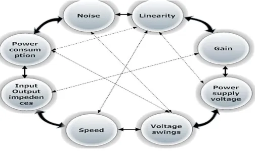
Functionality of integrated circuits of analog in nature is having profound significance that determines the performance of system. Functionaldescription encompasses necessities over the several measures that decides the performance of the circuit. The measures of functionality will be the parameters which will be utilized in illustration of the conduct of the small block analog nature. For the sample,the system that contains the amplifier circuitwill bedescribed with the help of rapidity, improvement in gain, utilization of power, proportionality and etc.,Achievement of entire group of measures of functionality will be frequentlychallenging and thereforeestablishes theinspiringcompromises in the formulation. The measures are characterized as the analog design octagon that is presented in Figure1 (Razavi, 2010) [2]
Evolving tools in the area of Electronic Design Automation, establishes the computerization of the procedureassociated with the design. The mentioned approach can be accomplished by providing the fresh formulation values for the parameters such as power, gain, slew rate etc., As an alternative of depending with the preceding information over the frameworks a specific structure of the circuit might be employed with the help of utilizing the freshly formulated strategies in exploration of the best solutions for the specified functions of motivation with the variability in conditions for providing the precise functionality.
Optimization of Design Techniques by Reducing
Power and Area of Two Stage CMOS Operational
Amplifier Employing Salp Swarm Algorithm
Figure 1. Analog design Octagon
Various suggestions are provided for the purpose of computerization formulation process of the circuit. These suggestions utilize the group of instructions depending with the previous information about the circuits with the provided group of stipulations. They are considered as tedious process since it involves the lot of tiresome human exertion to generate the fresh group of instructions for each process for the formulation of fresh circuit structure.[3]
Leakage current upsurges with the reduction in the size of the transistor. Enhanced compaction technique besides the unpurged requirements of leakage for very much least power consuming functioning that lies with the current restricted power formulation circumstances. Necessity of Power for mobile and portable functioning devices that is operated with the battery like handheld smart phone, clinical equipment will be much stricter with power. Minimization of power supply decreases the active power required by four time and the power that is getting leaked proportionally. Therefore, power supply reduction is the prominent concentration while performing the formulation of circuit with least power. The mentioned strategy causes the circuits functioning with the power supply voltage smaller than the required voltage for the proper operation of the transistor.
Dissipation of power is considered as significant challenge while performing the formulation of miniature sized circuits, particularly in transportable processing and individual areas of interaction with others such as mobile devices. Many advanced techniques that is currently existing is evolved with the motivation of designing with the dissipation of least power. low power dissipation in Very Large Integrated circuits techniques [4].
Two stages will be available in the formulation of circuit that will be analog nature [5]. Primary will be the development of the circuit structure and the next stage will be fine tuning the characteristics of the circuit for the purpose of formulation requirement, as provided by the user will eb termed as sizing of the circuit. Providing the proper dimension to the cell that will be fundamental block of the circuitwill be performed by the formulating the operational amplifier with the help of fine tuning the dimension of the transistor, supply currents and capacitor added for the compromising the performance of the
circuit. The above-mentioned technique will be the tedious procedure and in diverse techniques the dimensioning of the device will develop the assortedoutcomes. Therefore, computerized formulation procedure for the circuit of analog nature will be the indispensablefor the purpose of
accomplishment of solutions whichfulfill the
demandedfunctionalityalong with the leastexertion [6]. For theprovided structure of the circuit and stipulations, the dimensions and providing the operational conditions ofentire group of transistors must be considered in the style that the circuit satisfies the provided with the stipulations with the selection of best values for the parameters. While manufacturing the IC,the functionality of the circuit encounter certaindifferencesdeviated from the stipulated conditions. The mentioned deviations are the resulting because of the numerousmotives and the two significant faults will be listed as follows process variations and the mismatch [7]. The processes disparitiesin the approach will be resulted by means of changingthe operating conditions of procedure while performing the fabrication process and this mightdevelop the characteristics for procedure to modify. Generally, the characteristics for the procedure willbe presumed to take the analogous for entire set of transistors over the similarbase for fabrication, On the other hand it might fluctuate from different bases for the fabrication.Nonconformitywill beresulted because of the alterations that takes place locally over the similar chip, since the circuits of analog nature, depending with the exact appropriatenessof the group of transistors in addition with the alterations might deteriorate the functionality of the circuit. While the procedural fluctuations and the nonconformity will provide the direct impact over the functionality of the circuit of analog nature, functionalitythat pertains with the circuit might fall back in satisfying the proclaimed stipulations. Therefore, identification of the structured of the circuit and the group of formulation stipulations that are least responsive to the mentioned alterations [8].
Numerous Strategies were emerged to investigate the challenges that lies with the formulation of analog integrated circuits like ANACONDA [9], APE [10] optimization strategies utilized depending with the nature inspired evolutionary techniques, equation dependent symbolic investigation. With equation dependent investigations equations that pertains to the structure of the circuit will be utilized in the conversion of the design of analog integrated circuit into the function optimization issue with forgoing the concept of accuracy and processing steps that are involved.
Geometric Programming takes into consideration of the structure of the circuit structurer for the accomplishment of the solution that is globally best. Nevertheless, the mentioned technique consumesa greater number of processing stages in obtaining the group of designated expressions before providing the input to the optimization model.
Contrasting with the above-mentioned techniques heuristics
dependent exploit the
analog integrated circuit. Numerous Heuristics based strategies involved in the formulation of integrated circuits that are analog in nature will be discussed in the subsequent section.
II. LITERATURESURVEY
T
he problem with automatic selection of the sizing CMOS op-amp circuitwasestablished in the paper by Mandal and Viswanathan (2001) [11]. Provided with the circuit and thestipulations as prescribed, fundamental motivation lies in the identification of the size for the devices in an involuntary manner with the purpose of satisfying the provided stipulations for achieving the supreme functionality whereas reducing the expenditure involved in the process, like reducing the weighted addition of the dynamic dimension and dissipation of energy, The proposed strategy by Mandal and Viswanathan (2001) [11] wasrelied with observation by which the first order performance pertained to MOS transistor that functions in the area of saturation so as to simulate the expenditure and specified conditions as polynomials in the variable for the formulation in relation with the issue of identifying the best possible solution. The mentioned strategy is modelled as the convex optimization nature of the problem that can be utilized for identifying the best possible solution.For the purpose of determining the solutions to the problems related with the impact of second order, it should be dealt with the help of constructing the model of difficulty as the identification of solution to the series of convex programs. Statistical analysis observed the solution as the series of programs that will be in convex in nature congregateat thesimilar location of formulation for
thebroadlyfluctuatingpreliminaryassumptions. The mentioned strategy comprised the capability of identifying the solution that was approved as universally best for the provided challenge.
A Program utilizing the MATLAB for the purpose of establishing the involuntary symbolic generation of circuits of analog in nature comprising MOS transistors utilizing the strategy of altered analysis of nodes and optimization depending on ant colony strategy was proposed by the Shokouhifar and Jalali (2014) [12].Initially small signal models were generated for the entire MOS transistors and placed in the respective position of entire set of MOS transistors. Subsequently the investigation of circuit by providing the strategy of altered analysis of nodes, in addition with the production of equation for the provided circuit that exactly demonstrates the performance. The technique of optimization that is termed as Ant colony optimization was enforcedover the obtained equation for the purpose of simplification.For the purpose of reducing the mean square error (MSE) a fresh condition was established among the obtained expression and the attained expression that is simplified using Ant Colony Optimization. In the suggested technique the prominent merit lies in the fact that concludingrate of fault could be regulated and fine-tuned by the expert designer involved in the process.For the purpose of assessing the obtained solution produced by employing the
Ant Colony Optimization by computing the gain and phase margin at diverse range of frequencies.By providing the comparative analysis the achieved outcomes by utilizing the HSPCIE depicts the competence of the suggested strategy.
For the optimization of VLSI circuits Evolutionary techniques are preferred because of its simplicity, easiest approach and effective methodologies. In the paper, proposed by Sarkar et al., (2018) [13]. Aim of achieving the dimension that is optimum and the purpose of obtaining reduced offset voltage in the formulation of two step CMOS OP amp.is accomplished with the help of Whale Optimization Algorithm. The proposed design should satisfy diverse formulation conditions like Slew Rate, Open Loop Gain etc. will be provided that will be considered as additional conditions in the design of the operational amplifier. To manage current disparity during the output stage of the Operational Amplifier, offset reduction considered to be the significant need. Subsequently by reformulating the Operational Amplifier in the usual CADENCE Virtuoso circuit simulator technical outcomes of the process are confirmed. In between the simulated outcomes and the outcomes obtained through Whale Optimization Technique, there is a decent settlement is identified. The outcomes derived through the proposed WOA is then analyzed with the functionality of some other techniques that is utilized in the previous research papers. It is observed the WOA achieved better results for circuit dimension with lowest size in the design of CMOS Operational Amplifier for reduced offset as analyzed with other techniques Based on the comparative analyzed WOA Out classes all the other techniques by achieving a faster convergence, least power dissipation and reduced offset
For the purpose of minimization of the expenditure associated with design process of analog circuits and saving the time of the expert an optimized strategy was suggested The motivation of the current research by Dendouga et al., (2014) [14] existed in detailed explanation of the strategy depending with the Genetic Algorithms with many objectives in nature the multi-objective genetic algorithms (MOGAs) for the purpose of permitting the computerized design without the intervention of expertfor the circuits of analog and assorted (Combination of analog and in nature. For the purpose of obtaining the functionality of the operational amplifier,the suggested strategy involved in the determining the appropriate dimension of CMOS Transistorin addition with satisfying the conditions provided by the user for the proper operation of the circuit.To assess the design optimization techniques, six measures were taken into account. They are listed as, Direct Current (DC) Gain, Unity-Gain Bandwidth (GBW), Phase Margin (PM), Utilization of Power (P), Dimension (A), and slew rate (SR).
A computerized formulation tool that performs the optimization of the design technique was performed by Barros et al., (2010) [15] For the purpose of enhancing the performance of circuits of analog nature alteredkernel of
genetic algorithm.The
the optimization including theedges. Developing the model of Machine Learning along with distributed computational capacity, the proposed strategy was containing the capacity of handling the functions that will be multi-objective in nature along with the provision of large quantity of conditions for the purpose of providing the optimization. The strategy that is being evolved contained the modelling capacities along with the scalablestructure wereestablished. Enhancement in the formulation strategy was established for the purpose of providing the strong design technique involved in the utilization of CMOS operational amplifiers.Forenhancing the effectiveness of the techniques based on evolutionary approach, SVM was presented. Suggestedtechniquesledin the formulation of innovative GA-SVM trainingarrangement enforce with a view of formulating the circuits that might be analog in nature devised with the help of the communication
between the suggested machine learning
approaches.Furthermore,the technique was devised with the capacity of handling the fluctuations that took place in the process a characteristicthat pertains to the manufacturing procedurealong with fluctuating circumstance of functioning (supply voltage or temperature variations), a basic characteristic that was neededfor the achievement of the strong formulation.
A competent formulation strategy was projected by Maji by et al., (2018[16] for the usuallyutilized circuits of analog in nature, namely, CMOS current mirror load-based differential amplifier and CMOS Two-stage operational amplifier by using the CMOS transistor. To optimize the design process involved in the formulation of the circuit, combined evolutionarystrategy wasemployed that will be listed as Random Particle Swarm Optimization along with differential
evolution. (RPSODE). Random PSO employs the
biasedelementsto supervise the path of exploration.A strong evolutionary based strategy named as Differential Evolution is utilized. Which depicts the exceptional functioning for the issues related with the finding the best solution that provides the incessant strategy in addition with the provision of solution that is accepted universally. On the other hand, Differential Evolutionencounters the problems of ambiguous in nature. Though many advantages exploited by the PSO strategy, it encounters the issue ofobtaining the solution that will be
below par in nature was aroused. Thework
competentlycombines the Random PSO and DE for eradicating the mentioned restrictions associated with the strategies if applied independently. In this paper, RPSODE wasutilized for the purpose of providing the best selection strategy involved in the size selection mechanism of transistors for minimizing the area occupied by the circuit by fulfilling the conditions of the formulation.
III. PROBLEMFORMULATION
Analog circuit design is generally observed to be less reliable and more heuristic in nature than digital design due to variations in circuit device properties, different circuit schematics, design requirements and specifications. The presence of such variations leads to extreme conditions which
makes analog circuit design process a daunting task for a circuit designer. Every analog circuit design process comes with certain operating conditions (temperature, sup- ply voltages, bias currents etc.) and tradeoffs [17] among design specifications. The tradeoffs confine the circuit design to a solution space instead of a single solution. Circuit response bounded by these tradeoffs, can be formulated as an objective function for optimization process subject to a variety of circuit specifications. An example of such objective function can be seen in Equation 1.
𝑀𝑎𝑥𝑖𝑚𝑖𝑧𝑒 ℎ0(𝑥)
𝑠𝑢𝑏𝑗𝑒𝑐𝑡 𝑡𝑜 ℎ𝑘 𝑥 ≤ 1 𝑘𝜖𝑅
𝑝𝑖 𝑥 = 1 𝑖 𝜖 𝑅 (1)
𝑥𝑗 > 0 𝑗 > 2
Where
ℎ0(𝑥)istheobjectivefunctionandℎ𝑘 𝑥 ,𝑝𝑖 𝑥 &𝑥𝑗;denotedesign constraints.
IV. PROPOSEDMETHODOLOGY
In normal electronic circuits Operational amplifiers are the widely utilized device. Operational Amplifiers provide broad range of applications. Difficulty in proper design of the Operational Amplifiers is the deciding factor that affects the performance CMOS based circuits of analog in nature. While manufacturing the Operational Amplifier Integrated Circuits using the CMOS transistor, the fundamental motivation lies in the fact of reducing the area occupied by the device for the purpose of providing the compact design and reduction consumption of energy or to reduce unwanted wastage of power in dissipation. The challenge of designing and implementation of two stage CMOS Operation amplifier is the satisfactory performance by achieving the numerousfactors that will decide the overall performance of the circuit.
The circuit provided in the figure 2 comprise of two phases while phase 1contains the portion of differential amplifier and the stage 2 contains the portion of common source amplifier. Two Voltage inputs Vin+ and Vin- will be present in differential amplifier and the circuit functions by augmenting the values of difference provided by the two-voltage source. Common source amplifier is utilized in second stage for the purpose of amplifying the gain provided by the differential amplifier due to the fact that are obtained from the differential amplifier stage is not sufficient for the proper operation of the circuit. For the purpose of achieving the least quantity of gain at increased frequency in addition with retain the balancing the operation of the circuit inclusion of additional circuit that performs the function of compensation strategy while the amplifier is being operated in negative feedback structure [18]. Differential Amplifiers takes the position of the Primary Stage and Common Source Amplifiers takes the position of last stage in the Operational Amplifiers with the two stage. Amplifier which performs the
and Common Source Amplifier arrange additionally expands the gain and furthermore gives high yield voltage swing [19].
[image:5.612.50.295.250.417.2]In circuits where the gain given by the differential intensifier organize is insufficient, extra enhancement required is given by the second stage, i.e. the basic source amplifier, driven by the yield of the principal arrange. The biasing circuit gives the best possible working point to every transistor in its immersion area. A yield support stage can be appended toward the end to give the low yield impedance and bigger yield current expected to drive the heap. For a little capacitive load yield cradle is not required. At the point when the yield support organize is not utilized, the circuit goes about as an Operational Trans-conductance Amplifier or OTA. Circuit Diagram is shown in figure 2 and the constraints for the design are provided below.
Figure 2 Circuit Diagram of Two Stage Differential Amplifier Table 1 Constraints and Specification of Two Stage
Operational Amplifier
Constraints Specification
Open-loopgain(Adc)Unitygainb andwidth(w0)
Slewrate(SR)
Inputcommon-mode range(ICMR) OutputvoltageswingL
oad c a p a c i t a n c ePhaseM
argin
Maximize 5MHz
>
10V/µs---1to2V
±
2VlOpF
60deg
Power Dissipation ≤ 2000 μ watt For Optimization the design of Objective Function is most necessary stage and optimization algorithm will maximize or minimize the objective function otherwise called as Cost Function depending on the provides constraints and the focus is to find the optimum solution by satisfying all the
constraints. Objective Function may be single or multi objective [21].
Equation 2 is objective function or Cost Function 𝑂𝐹 𝑜𝑟 𝐶𝐹 = 𝑛𝑖=1(𝑊𝑖∗ 𝐿𝑖) (2)
AnOptimization of the design:
This section portrays the suggested optimization strategyfor the purpose of formulating analog circuits for certain design parameters through the nature inspired meta heuristic Salp Swarm Algorithm, SSA.
B Salp Swarm Algorithm
SSA is a unique meta-heuristic optimizer freshly developed by Mirjalili et al.,[21] for the purpose of competently handling the challenges lies in the optimization. Salp is categorized in the division of Salpidae group. The swarming behavior that exits in the salps is largely observed due to the development of cooperative chains while performing the hunting events in deep oceans. The mentioned conduct supports salps in the achievement of improved kinetic energy throughout following source of diet.
Combinedly functioning the strategy of Salps impacts the evolution of SSA technique via producing the path following mechanism of Swarms in the chained manner. The chain created by the group of Salps might help SSA in overcoming letharginess by getting trapped in the position of local optima (LO) for certain degree. Nevertheless, SSA might not perform the appropriate equilibrium among the investigation and implementation procedures. Consequently, the actual approach sporadically flops in achieving the highly supreme global optimum in certain actual circumstances.
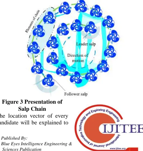
Two categories of the Salps are identified in Chain that is part of theSSA, that are termed as front-runner and cohorts. Positioned at the top of the chain will be the front runner and act as leader, whereas additional candidates are taking the position of supporters. Front-runner salp directs the course and movement of group, whereas the supporters exploit the utilization of additional peers. A theoretical formulation of salp chain is presented in Fig. 3.
Figure 3 Presentation of Salp Chain
[image:5.612.58.287.461.667.2] [image:5.612.320.564.523.782.2]investigatethe area of solution that contains the n-dimension, while n will be quantity of variables involved in the process of decision making. The population of SSA X will comprise of N salps with d-dimensions. Consequently, population vector is developed with the help of a N × d-dimensional matrix, as presented in Equation (3):
𝑋𝑖 =
𝑥11 𝑥21 … 𝑥12 𝑥22 …
⋮ ⋮ ⋱
𝑥𝑑1 𝑥𝑑2 ⋮ 𝑥1𝑁 𝑥2𝑁 … 𝑥𝑑𝑁
(3)
The destination position for the entire candidates in the group is identified as food source. Therefore, location pertains to front-runner will be attained with the help of Equation (4): 𝑥𝑗1
= 𝐹𝑗 + 𝑐1( 𝑢𝑏𝑗 − 𝑙𝑏𝑗 𝑐2+ 𝑙𝑏𝑗) 𝑐3≥ 0.5 𝐹𝑗 + 𝑐1( 𝑢𝑏𝑗 − 𝑙𝑏𝑗 𝑐2+ 𝑙𝑏𝑗) 𝑐3 < 0.5
(4)
while xj1 is the location of front-runner and Fj is the location
pertains to the food source source of food in the jth dimension, ubj is the higher boundary of jth dimension, and lbj is the lesser
boundary of jth dimension, c2 and c3 will be the arbitrary
vectors producing values within the range of[0, 1], and c1 will
be the fundamental characteristic of SSA articulated provided in Equation. (5),
𝑐1= 2 𝑒 − 4𝑡
(𝑇max )2
(5)
while t demonstrated the present iteration, and Tmax
demonstrates the least quantity of iterations. The previous characteristic c1 might develop the investigation and
implementation inclinations of SSA in the composed status. The location pertains to supportingcandidates are reviewed by Equation (6):
𝑥𝑗1=
𝑥𝑗1+ 𝑥𝑗1−1 2
(6)
The following section provides the algorithm flow that shows the SSA
Algorithm 1 – Salp Swarm Algorithm
Prepare the preliminary the salp population xi (i = 1, 2, ..., n) by taking into account ofub and lb
While (Not fulfilling the termination constraint)
Compute the suitabilitybelongs to every exploringcandidate (salp) F=the greatestexploringcandidate
Improve the c1 using Eq. (5)
For
Everycandidate (xi) if (i==1)
Improvelocation pertains to the candidate that takes the position as front funning with the help of Eq. (4)
Else
Improvelocationbelongs to the supporting candidate using Eq. (6)
end end
Modifycandidatesdepending with the highest and leastlimits of variables
end
return F
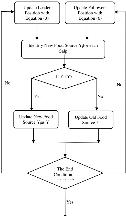
[image:6.612.325.571.88.511.2]Flow Chart of The SSA Algorithm Is Provided in Figure 4.
Figure 4. Flow chart of the SSA Algorithm
Methodology of Optimizing the Parameters Using SSA Algorithm
With respect to Algorithm 1 that is portrayed in the preceding section the SSA strategyarbitrarilyspreads the entire exploring candidates (salps) on the area meant of the solution. For the purpose of identifying the salt that will lead the group evaluation of the present group of salps. Entire group of salps attempt in pursuing theleader of the group. The mentioned process is presented in Fig. 3. The mentioned procedure, involved in enhancing the variablec1 is updated by Eq. (5). For the purpose of conveying the status of the front-runner.Theinstruction existed in Eq. (3) is utilized, whereas Eq. (5) will be involved in
altering the location of additional members of the
No No
Yes No
Yes Update Leader
Position with Equation (3)
Update Followers Position with
Equation (6)
Identify New Food Source Yifor each
Salp
If Yi<Y?
Update New Food Source Yias Y
Update Old Food Source Y
The End Condition is
group. Till fulfilling the criteria of termination, entirephaseswithout the starting phase might be applied for the purpose of improving the supremacy of obtained solution. The
[image:7.612.50.549.71.473.2]flowchart of the SSA-based Parameter Optimization approach is also shown in Fig. 5.[22]
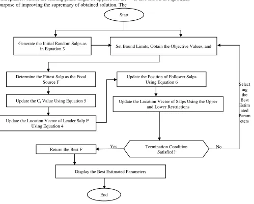
Figure 5. Flow chart of Proposed technique employed for the optimization of Parameter using SSA Algorithm
V. EXPERIMENTALRESULTS
A. SSA based Circuit Design:
Parameter values specified for the design proposal and for the selected technology (180 nm) is presented in Table (3). Using the system with CPU Intel core i7 that contains 4 GB RAM and MATLAB Software Package version 7.5, Simulations are carried out. For the proposed SSA algorithm, total quantity of search agents selected are 50 and the dimension Chosen is 10 i.e. the design variables picked for the proposed circuit are 7. Highest number of iterations selected for the recommended technique is 100.
TABLE 2
TECHNOLOGY PARAMETERS, INPUTS AND LENGTH OF MOS S. No Specification Values used
1 VDD(V) 2.5
2 VSS (V) -2.5
3 VtP(V) -0.39
4 Vtn(V) 0.35
5 K’N' (µA/V2) 177.2
6 K’P(µA/V2) 35.6
7 Length (µm) 0.18
TABLE 3
DESIGN PARAMETERS OBTAINED WITH DIFFERENT ALGORITHMS FOR THE
OPAMP
Design Parameters
SSA CGWO GA
IBIAS (µA) 21.8 22.2 34.5
Cc 2.018 2.2 pf 2.4 pf
W1/L1 8=1.44/0.18 8=1.44/0.18 2/0.18 W2/L2 8=1.44/0.18 8=1.44/0.18 2/0.18 W3/L3 4=0.72/.18 4=0.72/.18 4/018 W4/L4 4=0.72/0.18 4=0.72/0.18 4/0.18 W5/L5 1=0.4/0.4 1=0.4/0.4 2/0.18 W6/L6 40=7.20/0.18 40=7.20/0.18 22.64/0.18 W7/L7 8=1.44/0.18 8=1.44/0.18 8/0.18
TABLE 5
DESIGN SPECIFICATIONS OBTAINED WITH DIFFERENT ALGORITHMS FOR THE
OPAMP. Design
Criteria
Specifications SSA CGWO GA Start
Generate the Initial Random Salps as
in Equation 3 Set Bound Limits, Obtain the Objective Values, and
Determine the Fittest Salp as the Food Source F
Update the Position of Follower Salps Using Equation 6
Update the Ci Value Using Equation 5 Update the Location Vector of Salps Using the Upper
and Lower Restrictions
Update the Location Vector of Leader Salp F Using Equation 4
Return the Best F Termination Condition Satisfied?
Yes No
Display the Best Estimated Parameters
Select ing the Best Estim ated Param eters
[image:7.612.82.264.648.737.2]Slew Rate (V// μs
≥ 10 V / μs 24 20 15
Load Capacitance
CL (pf)
≥ 10 pf 15 12 9
Gain in dB 40 dB 39.89 39.64 36.48 Unity Gain
Bandwidth MHz
≥ 5 MHZ 19.32 18.43 16.54
VIc (min) ≥ -1.5v -0.01 -0.01 -0.2
VIc (max) ≤ 2V 1.47 1.10 1.01
Power Dissipation
Pdiss (µw)
≤ 2000 μ watt 67 72 117
Total Area ≤180 µm2 65.7 71.26 94.7 Phase
Margin in Degree
≥60 Degree 59.24 58.6 48.4
CMRR ≥60 dB 142.35 134.6 133.7
PSRR ≥60 dB 184.17 180 179.1
The fundamental motivation of the technique is the minimization of the dimension Occupied and dissipation of power. For the purpose of accomplishment of the best circuit sizing for two phase CMOS Operational Amplifiers, SSA technique is applied for the selection of Optimal sizes that pertains to the MOS transistors along with Load Capacitance and Compensation Capacitance. Along with the operation proposed algorithm so that it satisfies specified formulation characteristics and constraints specified for the design. The parameter values for the selected technology, values for the power supply and the boundaries of design parameters and specifications are provided as inputs for Optimization Algorithm.The obtained values are obtained listed in Table and compared with other techniques utilized for the optimization. It is observed that the proposed optimization procedure performs far superior than the other techniques utilized in the optimization of design.
VI. CONCLUSION
A techniquefor the purpose of design optimization of the analog circuit optimization utilizing a nature inspired meta heuristic technique named as salp swarm Algorithm is proposed and the efficiency of the suggested technique is revealed by verifying the solutions of a two-stage differential amplifier circuit. With the help of observation of the results obtained that were tabulated in table 3 and table 4 it is inferred that by adopting the optimal dimension of transistors which works with 180nm technology least power dissipationof 67µ watt is obtained utilizing the Salp Swarm Optimization technique.By Performing the analysis of the proposed technique, it is observed that bycomparing the solutions of suggestedapproach SSA along withadditional optimization techniques utilized for the same purpose, the recommended SSA approach is better in providing quality solutions without affecting the rate of convergence because of the multiple constraint handling capability concurrently in the significant manner.
REFERENCES
1. Barari, M., Karimi, H. R., &Razaghian, F. (2014). Analog circuit design optimization based on evolutionary algorithms. Mathematical Problems in Engineering, 2014.
2. Behzad Razavi (2010), Design of Analog CMOS Integrated Circuits, McGraw-Hill, Inc. New York, NY, USA
3. Joshi, D., Dash, S., Agarwal, U., Bhattacharjee, R., & Trivedi, G. (2015, December). Analog circuit optimization based on hybrid particle swarm optimization. In 2015 International Conference on Computational Science and Computational Intelligence (CSCI) (pp. 164-169). IEEE. 4. Bendre, V., &Kureshi, A. K. (2015, February). An overview of various
leakage power reduction techniques in deep submicron technologies. In 2015 International Conference on Computing Communication Control and Automation (pp. 992-998). IEEE.
5. Sabat, S. L., Kumar, K. S., &Udgata, S. K. (2009, December). Differential evolution and swarm intelligence techniques for analog circuit synthesis. In 2009 World Congress on Nature & Biologically Inspired Computing (NaBIC) (pp. 469-474). IEEE.
6. Alpaydin, G., Balkir, S., &Dundar, G. (2003). An evolutionary approach to automatic synthesis of high-performance analog integrated circuits. IEEE Transactions on Evolutionary Computation, 7(3), 240-252. 7. Hastings, R. A., & Hastings, R. A. (2006). The art of analog layout (Vol.
2). New Jersey: Pearson Prentice Hall.
8. Kumar, P., &Duraiswamy, K. (2012). An optimized device sizing of analog circuits using particle swarm optimization. In Proceedings of IEEE International Conference on Neural Networks, Nov. 27-Dec. 1, IEEE Xplore.
9. Phelps, R., Krasnicki, M., Rutenbar, R. A., Carley, L. R., &Hellums, J. R. (2000). Anaconda: simulation-based synthesis of analog circuits via stochastic pattern search. IEEE Transactions on Computer-Aided Design of Integrated Circuits and Systems, 19(6), 703-717.
10.Venkatesh, G. (2013, June). APE: Accelerator processor extensions to optimize data-compute co-location. In Proceedings of the ACM SIGPLAN Workshop on Memory Systems Performance and Correctness (p. 1). ACM.
11.Mandal, P., & Visvanathan, V. (2001). CMOS op-amp sizing using a geometric programming formulation. IEEE Transactions on Computer-Aided Design of Integrated circuits and systems, 20(1), 22-38.
12.Shokouhifar, M., &Jalali, A. (2014, May). Automatic symbolic simplification of analog circuits in MATLAB using ant colony optimization. In 2014 22nd Iranian Conference on Electrical Engineering (ICEE) (pp. 407-412). IEEE.
13.Sarkar, P., Laskar, N. M., Nath, S., Baishnab, K. L., & Chanda, S. (2018). Offset voltage minimization-based circuit sizing of CMOS operational amplifier using whale optimization algorithm. Journal of Information and Optimization Sciences, 39(1), 83-98.
14.Dendouga, A., Oussalah, S., Thienpont, D., &Lounis, A. (2014). Multiobjective genetic algorithms program for the optimization of an OTA for front-end electronics. Advances in Electrical Engineering, 2014.
15.Barros, M., Guilherme, J., & Horta, N. (2010). Analog circuits optimization based on evolutionary computation techniques. Integration, 43(1), 136-155.
16.De, B. P., Maji, K. B., Kar, R., Mandal, D., & Ghoshal, S. P. (2018). Design of optimal cmos analog amplifier circuits using a hybrid evolutionary optimization technique. Journal of Circuits, Systems and Computers, 27(02), 1850029.
17.Allen, P. E., &Holberg, D. R. (1987). CMOS analog circuit design. Oxford university press.
18.Kavyashree, C. L., Hemambika, M., Dharani, K., Naik, A. V., & Sunil, M. P. (2017, January). Design and Implementation of two stage CMOS Operational amplifier using 90nm technology. In 2017 International Conference on Inventive Systems and Control (ICISC) (pp. 1-4). IEEE. 19.Sharma, A., Jangra, P., Kumar, S., & Yadav, R. (2017). Design and
Implementation of Two Stage CMOS Operational Amplifier. International Research Journal
20.Mirjalili, S., Gandomi, A. H., Mirjalili, S. Z., Saremi, S., Faris, H., &Mirjalili, S. M. (2017). Salp Swarm Algorithm: A bio-inspired optimizer for engineering design problems. Advances in Engineering Software, 114, 163-191.